


QUICK LOGIC QL8025-7PT196I, QL8025-7PT196M, QL8025-7PV100C, QL8025-7PV100I, QL8025-7PV100M Datasheet
...' / +
& & , # " "-" . " +. "
0.18 , six layer metal CMOS process
1.8 V Vcc, 1.8/2.5/3.3 V drive capable I/O
Up to 4,008 dedicated flip-flops
Up to 55.3 K embedded RAM Bits
Up to 313 I/O
Up to 370 K system gates
IEEE 1149.1 Boundary Scan Testing Compliant
Low Power Capability
Up to twenty-four 2,304 bit Dual Port High Performance SRAM Blocks
Up to 55,296 embedded RAM bits
RAM/ROM/FIFO Wizard for automatic configuration
Configurable and cascadable
!
High performance I/O cell with Tco< 3 ns
Programmable Slew Rate Control
Programmable I/O Standards:
LVTTL, LVCMOS, LVCMOS18, PCI, GTL+, SSTL2, and SSTL3
Independent I/O Banks capable of supporting multiple standards in one device
I/O Register Configurations: Input, Output, Output Enable (OE)
" #$% &$
Multiple dedicated Low Skew Clock Networks
High drive input-only networks
Quadrant-based segmentable clock networks
User Programmable Phase Locked Loops
# ' " ("
) #( *
Hardwired DSP building blocks with integrated Multiply, Add, and Accumulate Functions.
+
The QuickLogic products come with secure ViaLink technology that protects intellectual property from design theft and reverse engineering. No external configuration memory needed; Instant-on at Power-up.
PLL |
Embedded RAM Blocks |
PLL |
|
Embeded Computational Units |
|
|
Fabric |
|
PLL |
Embedded RAM Blocks |
PLL |
|
|
|
Preliminary

|
|
|
1 3405 |
1 3454 |
1 3 54 |
1 3054 |
1 3605 |
|
|
|
|
|
|
|
|
|
Max Gates |
47,052 |
63,840 |
188,946 |
248,160 |
320,640 |
|
|
|
|
|
|
|
|
|
Logic Array |
16 x 8 |
16 x 16 |
32 x 20 |
40 x 24 |
48 x 32 |
||
|
|
|
|
|
|
|
|
|
Logic Cells |
128 |
256 |
640 |
960 |
1,536 |
|
|
|
|
|
|
|
|
|
Max Flip-Flops |
526 |
884 |
1,697 |
2,670 |
4,002 |
||
|
|
|
|
|
|
|
|
|
Max I/O |
90 |
124 |
139 |
250 |
310 |
|
|
|
|
|
|
|
|
|
RAM Modules |
4 |
4 |
16 |
20 |
24 |
||
|
|
|
|
|
|
|
|
|
RAM Bits |
9,216 |
9,216 |
36,864 |
46,100 |
55,300 |
|
|
|
|
|
|
|
|
|
|
PLLs |
0 |
0 |
0 |
4 |
4 |
|
|
|
|
|
|
|
|
|
|
ECUs |
0 |
0 |
0 |
10 |
12 |
|
|
|
|
|
|
|
|
|
|
|
VQFP |
100 |
100 |
100 |
- |
- |
|
|
|
|
|
|
|
|
|
|
CSBGA (0.8 mm) |
196 |
196 |
196 |
- |
- |
|
|
|
|
|
|
|
|
Packages |
|
PQFP |
208 |
208 |
208 |
208 |
208 |
|
|
|
|
|
|
|
|
|
|
FBGA (0.8 mm) |
- |
- |
- |
280 |
280 |
|
|
|
|
|
|
|
|
|
|
BGA (1.0 mm) |
- |
- |
- |
484 |
484 |
|
|
|
|
|
|
|
|
!" #$! % & &
|
44 71 |
89 # :, |
043 1 |
034 # :, |
;3; :, |
|
|
|
|
|
|
QL8025 |
62 |
90 |
90 |
- |
- |
|
|
|
|
|
|
QL8050 |
62 |
100 |
124 |
- |
- |
|
|
|
|
|
|
QL8150 |
62 |
100 |
139 |
- |
- |
|
|
|
|
|
|
QL8250 |
- |
- |
115 |
163 |
250 |
|
|
|
|
|
|
QL8325 |
- |
- |
115 |
163 |
310 |
|
|
|
|
|
|
1$2$"-&
The QuickWorks package provides the most complete ESP and FPGA software solution from design entry to logic synthesis, to place and route, and simulation. The package provides a solution for designers who use third party tools from Cadence, Mentor, OrCAD, Synopsys, Viewlogic, and other third-party tools for design entry, synthesis, or simulation.
Eclipse-II is fabricated on a 0.18 , six layer metal CMOS process. The core voltage is
1.8 V Vcc supply and the I/Os are up to 3.3 V tolerant. The Eclipse-II product line is available in commercial, industrial, and military temperature grades.
0 Preliminary

! &
The Eclipse-II logic cell structure is presented in 0. This architectural feature addresses today's register-intensive designs.
0 1 & , &
" " |
' " |
& ' , |
' , |
|
|
|
|
Multiplexer |
16:1 |
5 ns |
2.8 ns |
|
|
|
|
Parity Tree |
24 |
6 ns |
3.4 ns |
|
|
|
|
Counter |
36 |
6 ns |
3.4 ns |
|
|
|
|
|
16 bit |
250 MHz |
450 MHz |
|
|
|
|
|
32 bit |
250 MHz |
450 MHz |
|
|
|
|
FIFO |
128 x 32 |
155 MHz |
280 MHz |
|
|
|
|
|
256 x 16 |
155 MHz |
280 MHz |
|
|
|
|
|
128 x 64 |
155 MHz |
280 MHz |
|
|
|
|
Clock-to-Out |
|
4.5 ns |
2.5 ns |
|
|
|
|
System clock |
|
200 MHz |
400 MHz |
|
|
|
|
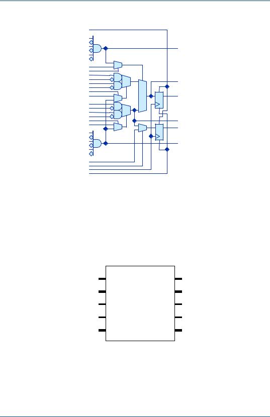
The Eclipse-II logic cell structure presented in 0 is a dual register, multiplexor-based logic cell. It is designed for wide fan-in and multiple, simultaneous output funtions. Both registers share CLK, SET, and RESET inputs. The second register has a two-to-one multiplexer controlling its input. The register can be loaded from the NZ output or directly from a dedicated input.
NOTE: ' & & & ( & ( & ' & & ' & ' ' ' )*+ ,-& & ' . + / '
& & & & && & ' &&
The complete logic cell consists of two 6-input AND gates, four two-input AND gates, seven two- to-one multiplexers, and two D flip-flops with asynchronous SET and RESET controls. The cell has a fan-in of 30 (including register control lines), fits a wide range of functions with up to 17 simultaneous inputs, and has six outputs (four combinatorial and two registered). The high logic capacity and fan-in of the logic cell accommodates many user functions with a single level of logic delay while other architectures require two or more levels of delay.
|
Preliminary |
|
|
|
6 |
||
|
|
|
|
|
|
|
||
|
QS |
|
|
A1 |
|
|
A2 |
|
|
A3 |
AZ |
|
A4 |
||
|
||
A5 |
|
|
A6 |
|
|
OS |
|
|
OP |
|
|
B1 |
|
|
B2 |
OZ |
|
C1 |
||
|
||
C2 |
|
|
MP |
|
|
MS |
QZ |
|
D1 |
|
|
D2 |
|
|
E1 |
|
|
E2 |
|
|
NP |
NZ |
|
NS |
Q2Z |
|
F1 |
||
|
||
F2 |
|
|
F3 |
FZ |
|
F4 |
||
F5 |
|
|
F6 |
|
|
PS |
|
|
PP |
|
|
QC |
|
|
QR |
|
|
|
|
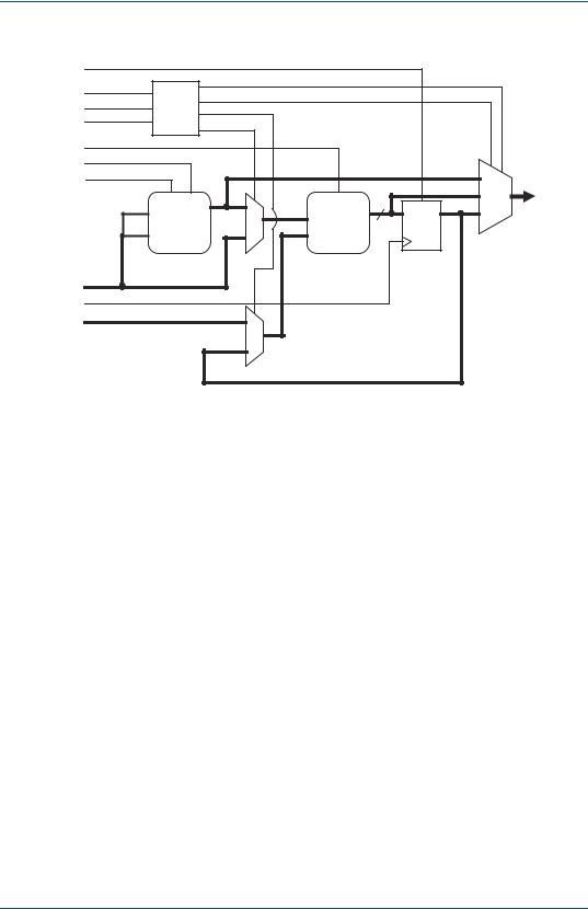
The Eclipse-II Product Family includes up to 24 dual-port 2,304-bit RAM modules for implementing RAM, ROM, and FIFO functions. Each module is user-configurable into four different block organizations and can be cascaded horizontally to increase their effective width, or vertically to increase their effective depth as shown in ;.
2,304-bit RAM Module
MODE[1:0] ASYNCRD
WA[9:0] RA[9:0]
WD[17:0] RD[17:0]
WE |
RE |
WCLK RCLK
!" " #
The number of RAM modules varies from 4 to 24 blocks for a total of 9.2 K to 55.3 K bits of RAM. Using two "mode" pins, designers can configure each module into 128 x 18 (Mode 0), 256 x 9 (Mode 1), 512 x 4 (Mode 2), or 1024 x 2 blocks (Mode 3). The blocks are also easily cascadable to increase their effective width and/or depth (see ;).
; Preliminary
WDATA |
RAM |
RDATA |
|
Module |
|
WADDR (2,304 bits)
 RADDR
RADDR
RAM
Module
WDATA (2,304 bits)
 RDATA
RDATA
# # !" " #
The RAM modules are dual-port, with completely independent READ and WRITE ports and separate READ and WRITE clocks. The READ ports support asynchronous and synchronous operation, while the WRITE ports support synchronous operation. Each port has 18 data lines and 10 address lines, allowing word lengths of up to 18 bits and address spaces of up to 1,024 words. Depending on the mode selected, however, some higher order data or address lines may not be used.
The Write Enable (WE) line acts as a clock enable for synchronous write operation. The Read Enable (RE) acts as a clock enable for synchronous READ operation (ASYNCRD input low), or as a flow-through enable for asynchronous READ operation (ASYNCRD input high).
Designers can cascade multiple RAM modules to increase the depth or width allowed in single modules by connecting corresponding address lines together and dividing the words between modules.
A similar technique can be used to create depths greater than 512 words. In this case address signals higher than the ninth bit are encoded onto the write enable (WE) input for WRITE operations. The READ data outputs are multiplexed together using encoded higher READ address bits for the multiplexer SELECT signals.
The RAM blocks can be loaded with data generated internally (typically for RAM or FIFO functions) or with data from an external PROM (typically for ROM functions).
# ' " (" ) #(*
Traditional Programmable Logic architectures do not implement arithmetic functions efficiently or effectively—these functions require high logic cell usage while garnering only moderate performance results.
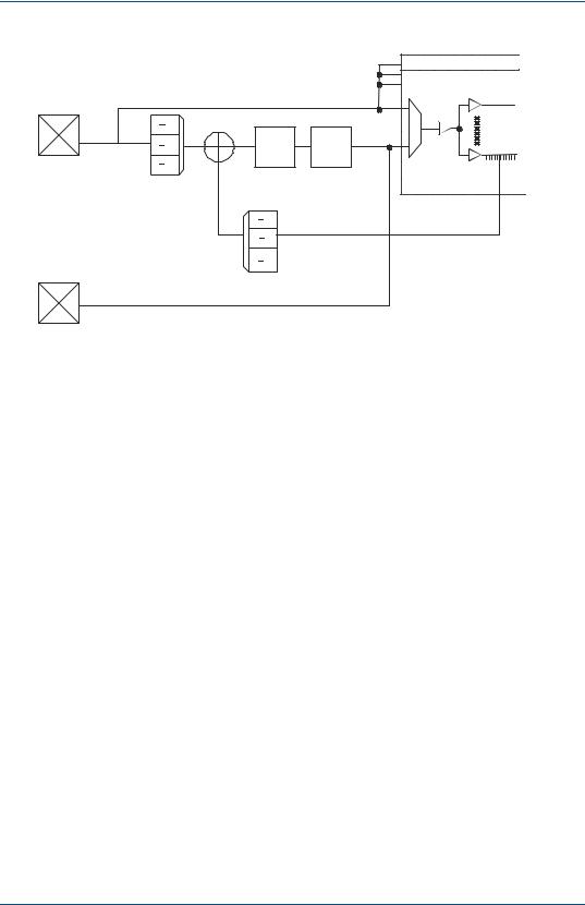
The Eclipse-II architecture allows for functionality above and beyond that achievable using programmable logic devices. By embedding a dynamically reconfigurable computational unit, the Eclipse-II device can address various arithmetic functions efficiently. This approach offers greater performance than traditional programmable logic implementations. The embedded block is implemented at the transistor level as shown in 5.
|
Preliminary |
|
|
|
5 |
||
|
|
|
|
|
|
|
||
|
RESET |
|
|
|
|
|
|
|
|
|
|
|
D |
|
|
|
|
|
S1 |
|
3-4 |
C |
|
|
|
|
|
S2 |
|
B |
|
|
|
|
|
|
|
decoder |
|
|
|
|
|
||
S3 |
|
A |
|
|
|
|
|
|
|
|
|
|
|
|
|
||
CIN |
|
|
|
|
|
|
|
|
SIGN1 |
|
|
|
|
|
|
|
|
SIGN2 |
|
|
|
|
|
|
00 |
Q[16:0] |
|
|
|
|
|
|
|
|
|
|
|
|
|
|
|
|
01 |
3-1 |
|
|
|
|
|
|
|
|
mux |
|
A[7:0] |
8-bit |
2-1 |
16-bit |
D |
Q |
10 |
|
|
|
17-bit |
|
|
|
|||
|
|
Multiplier |
mux |
Adder |
|
|
|
|
|
A[15:8] |
Register |
|
|
||||
|
|
|
|
|
|
|||
A[0:15] |
|
|
|
|
|
|
|
|
CLK |
|
|
|
|
|
|
|
|
B[0:15] |
|
|
2-1 |
|
|
|
|
|
|
|
|
|
|
|
|
|
|
|
|
|
mux |
|
|
|
|
|
|
|
|
$% |
|
|
|
||
The Eclipse-II ECU blocks ( < ;) are placed next to the SRAM circuitry for efficient memory/instruction fetch and addressing for DSP algorithmic implementations.
2 %3 4
|
#( |
|
|
QL8325 |
12 |
|
|
QL8250 |
10 |
|
|
QL8150 |
0 |
|
|
QL8050 |
0 |
|
|
QL8025 |
0 |
|
|
Up to twelve 8-bit MAC functions can be implemented per cycle for a total of 1 billion MACs/s when clocked at 100 MHz. Additional multiply-accumulate functions can be implemented in the programmable logic.
9 Preliminary

The modes for the ECU block are dynamically re-programmable through the programmable logic.
7 %3 , %
" " |
!' " |
#(-" . /= 2## |
|||||
|
0 |
6 |
|
( |
#! |
||
|
|||||||
0 |
0 |
0 |
Multiply |
6.6 ns max |
|
|
|
|
|
|
|
|
|
|
|
0 |
0 |
1 |
Multiply-Add |
8.8 ns max |
|
|
|
|
|
|
|
|
|
|
|
0 |
1 |
0 |
Accumulateb |
|
3.9 ns min |
1.2 ns max |
|
0 |
1 |
1 |
Add |
3.1 ns max |
|
|
|
|
|
|
|
|
|
|
|
1 |
0 |
0 |
Multiply (registered)c |
|
9.6 ns min |
1.2 ns max |
|
1 |
0 |
1 |
MultiplyAdd (registered) |
|
9.6 ns min |
1.2 ns max |
|
|
|
|
|
|
|
|
|
1 |
1 |
0 |
Multiply - Accumulate |
|
9.6 ns min |
1.2 ns max |
|
|
|
|
|
|
|
|
|
1 |
1 |
1 |
Add (registered) |
|
3.9 ns min |
1.2 ns max |
|
|
|
|
|
|
|
|
|
a.tPD, tSU and tCO do not include routing paths in/out of the ECU block.
b.Internal feedback path in ECU restricts max clk frequency to 238 MHz.
c.B [15:0] set to zero.
NOTE: & & &< 5& 5 6 % % & &
$' ) * "-"
Instead of requiring extra components, designers simply need to instantiate one of the preconfigured models (described in this section). The QuickLogic built-in PLLs support a wider range of frequencies than many other PLLs. These PLLs also have the ability to support different ranges of frequency multiplications or divisions, driving the device at a faster or slower rate than the incoming clock frequency. When PLLs are cascaded, the clock signal must be routed off-chip through the PLLPAD_OUT pin prior to routing into another PLL; internal routing cannot be used for cascading PLLs.
PLLs achieve a very short clock-to-out time—generally less than 3 ns. This low clock-to-out time is achieved by the PLL subtracting the clock tree delay through the feedback path, effectively making the clock tree delay zero.
|
Preliminary |
|
|
|
= |
||
|
|
|
|
|
|
|
||
|
9 illustrates a QuickLogic PLL.
1st Quadrant
2nd Quadrant 3rd Quadrant
Frequency Divide |
PLL Bypass |
4th Quadrant |
FIN |
|
|
. |
|
|
Clock |
.1 |
|
|
|
|
|
|
Tree |
. |
+ |
Filter |
vco |
.2 |
|
||
. |
|
- |
|
.4 |
|
|
Frequency Multiply
..1
..2
..4
FOUT
& '
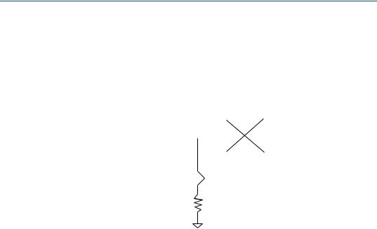
Fin represents a very stable high-frequency input clock and produces an accurate signal reference. This signal can either bypass the PLL entirely, thus entering the clock tree directly, or it can pass through the PLL itself.
Within the PLL, a voltage-controlled oscillator (VCO) is added to the circuit. The external Fin signal and the local VCO form a control loop. The VCO is multiplied or divided down to the reference frequency, so that a phase detector (the crossed circle in 9) can compare the two signals. If the phases of the external and local signals are not within the tolerance required, the phase detector sends a signal through the charge pump and loop filter ( 9). The charge pump generates an error voltage to bring the VCO back into alignment, and the loop filter removes any high frequency noise before the error voltage enters the VCO. This new VCO signal enters the clock tree to drive the chip's circuitry.
Fout represents the clock signal emerging from the output pad (the output signal PLLPAD_OUT is explained in < =). This clock signal is meaningful only when the PLL is configured for external use; otherwise, it remains in high Z state.
Most QuickLogic products contain four PLLs. The PLL presented in 9 controls the clock tree in the fourth quadrant of its FPGA. QuickLogic PLLs compensate for the additional delay created by the clock tree itself, as previously noted, by subtracting the clock tree delay through the feedback path.
For more specific information on the Phase Locked Loops, please refer to QuickLogic Application Note 58.
-!' "
QuickLogic PLLs have eight modes of operation, based on the input frequency and desired output frequency—< 9 indicates the features of each mode.
3 Preliminary

NOTE: (8 ( & 1 (' ' 1 & ( & (9 ( & 1 ( 1 & (
> 99 &
|
! ' |
"' > " + " |
! ' > " + " |
|
> " + |
||||
|
|
|
||
|
|
|
|
|
PLL_HF |
Same as input |
66 MHz–150 MHz |
66 MHz–150 MHz |
|
|
|
|
|
|
PLL_LF |
Same as input |
25 MHz–133 MHz |
25 MHz–133 MHz |
|
|
|
|
|
|
PLL_MULT2HF |
2x |
50 MHz–125 MHz |
100 MHz–250 MHz |
|
|
|
|
|
|
PLL_MULT2LF |
2x |
16 MHz–50 MHz |
32 MHz–100 MHz |
|
|
|
|
|
|
PLL_DIV2HF |
1/2x |
100 MHz–250 MHz |
50 MHz–125 MHz |
|
|
|
|
|
|
PLL_DIV2LF |
1/2x |
50 MHz–100 MHz |
25 MHz–50 MHz |
|
|
|
|
|
|
PLL_MULT4 |
4x |
16 MHz–40 MHz |
64 MHz–160 MHz |
|
|
|
|
|
|
PLL_DIV4 |
1/4x |
100 MHz–300 MHz |
25 MHz–75 MHz |
|
|
|
|
|
The input frequency can range from 16 MHz to 300 MHz, while output frequency ranges from 25 MHz to 250 MHz. When you add PLLs to your top-level design, be sure that the PLL mode matches your desired input and output frequencies.
"
< = summarizes the key signals in QuickLogic's PLLs.
5 . 9 99 , &
" % |
' " |
|
|
PLLCLK_IN Input clock signal
Active High Reset If PLL_RESET is asserted, then CLKNET_OUT and PLL_RESET PLLPAD_OUT are reset to 0. This signal must be asserted and then released
in order for the LOCK_DETECT to work.
PLL output This signal selects whether the PLL will drive the internal clock
ONn_OFFCHIP
network or be used off-chip. This is a static signal, not a dynamic signal. Tied to GND = outgoing signal drives internal gates.
Tied to VCC = outgoing signal used off-chip.
Out to internal gates This signal bypasses the PLL logic before driving the CLKNET_OUT internal gates. Note that this signal cannot be used in the same quadrant where
the PLL signal is used (PLLCLK_OUT).
PLLCLK_OUT
Out from PLL to internal gates This signal can drive the internal gates after going through the PLL. For this to work, ONn_OFFCHIP must be tied to GND.
PLLPAD_OUT
Out to off-chip This outgoing signal is used off-chip. For this to work,
ONn_OFFCHIP signal must be tied to VCC.
Active High Lock detection signal NOTE: For simulation purposes, this LOCK_DETECT signal gets asserted after 10 clock cycles. However, it can take a maximum of 200 clock cycles to sync with the input clock upon release of the RESET signal.
NOTE: 4 99%9:; * & 99;< , & '$99; * /#= & 99 /#;"3 ' "3 /#= & '$& &
|
Preliminary |
|
|
|
8 |
||
|
|
|
|
|
|
|
||
|

! #
Eclipse-II features a variety of distinct I/O pins to maximize performance, functionality, and flexibility with bi-directional I/O pins and input-only pins. All input and I/O pins are 1.8 V, 2.5 V, and 3.3 V tolerant and comply with the specific I/O standard selected. For single ended I/O standards, VCCIO specifies the input tolerance and the output drive. For voltage referenced I/O standards (e.g SSTL), the voltage supplied to the INREF pins in each bank specifies the input switch point. For example, the VCCIO pins must be tied to a 3.3 V supply to provide 3.3 V compliance. Eclipse-II can also support the LVDS and LVPECL I/O standards with the use of external resistors ( see < 3).
? !" , & & / &
! " |
-" 7 |
! ' 7 |
'' " |
|
|
|
|
LVTTL |
n/a |
3.3 V |
General Purpose |
|
|
|
|
LVCMOS25 |
n/a |
2.5 V |
General Purpose |
|
|
|
|
LVCMOS18 |
n/a |
1.8 V |
General Purpose |
|
|
|
|
PCI |
n/a |
3.3 V |
PCI Bus Applications |
|
|
|
|
GTL+ |
1 |
n/a |
Backplane |
|
|
|
|
SSTL3 |
1.5 |
3.3 V |
SDRAM |
|
|
|
|
SSTL2 |
1.25 |
2.5 V |
SDRAM |
|
|
|
|
As designs become more complex and requirements more stringent, several application-specific I/O standards have emerged for specific applications. I/O standards for processors, memories, and a variety of bus applications have become commonplace and a requirement for many systems. In addition, I/O timing has become a greater issue with specific requirements for setup, hold, clock to out, and switching times. Eclipse-II has addressed these new system requirements and now includes a completely new I/O cell which consists of programmable I/Os as well as a new cell structure consisting of three registers—Input, Output, and OE.
Eclipse-II offers banks of programmable I/Os that address many of the bus standards that are popular today. As shown in = each bi-directional I/O pin is associated with an I/O cell which features an input register, an input buffer, an output register, a three-state output buffer, an output enable register, and 2 two-to-one output multiplexers.
4 Preliminary
|
|
|
+ |
|
|
|
- |
INPUT |
Q |
E |
|
REGISTER |
|
|
D |
|
|
R |
|
|
|
|
PAD |
OUTPUT |
|
|
Q |
D |
|
|
|
REGISTER |
|
|
|
|
|
R |
|
|
|
E |
Q |
OUTPUT ENABLE |
D |
|
|
REGISTER |
|
R |
|
|
|
|
( )*
The bi-directional I/O pin options can be programmed for input, output, or bi-directional operation. As shown in =, each bi-directional I/O pin is associated with an I/O cell which features an input register, an input buffer, an output register, a three-state output buffer, an output enable register, and 2 two-to-one multiplexers. The select lines of the two-to-one multiplexers are static and must be connected to either Vcc or GND.
For input functions, I/O pins can provide combinatorial, registered data, or both options simultaneously to the logic array. For combinatorial input operation, data is routed from I/O pins through the input buffer to the array logic. For registered input operation, I/O pins drive the D input of input cell registers, allowing data to be captured with fast set-up times without consuming internal logic cell resources. The comparator and multiplexor in the input path allows for native support of I/O standards with reference points offset from traditional ground.
For output functions, I/O pins can receive combinatorial or registered data from the logic array. For combinatorial output operation, data is routed from the logic array through a multiplexer to the I/O pin. For registered output operation, the array logic drives the D input of the output cell register which in turn drives the I/O pin through a multiplexer. The multiplexer allows either a combinatorial or a registered signal to be driven to the I/O pin. The addition of an output register will also decrease the Tco. Since the output register does not need to drive the routing the length of the output path is also reduced.
The three-state output buffer controls the flow of data from the array logic to the I/O pin and allows the I/O pin to act as an input and/or output. The buffer's output enable can be individually controlled by the logic cell array or any pin (through the regular routing resources), or it can be bank-controlled through one of the global networks. The signal can also be either combinatorial
|
Preliminary |
|
|
|
|
||
|
|
|
|
|
|
|
||
|

or registered. This is identical to that of the flow for the output cell. For combinatorial control operation data is routed from the logic array through a multiplexer to the three-state control. The IOCTRL pins can directly drive the OE and CLK signals for all I/O cells within the same bank.
For registered control operation, the array logic drives the D input of the OE cell register which in turn drives the three-state control through a multiplexer. The multiplexer allows either a combinatorial or a registered signal to be driven to the three-state control.
When I/O pins are unused, the OE controls can be permanently disabled, allowing the output cell register to be used for registered feedback into the logic array.
I/O cell registers are controlled by clock, clock enable, and reset signals, which can come from the regular routing resources, from one of the global networks, or from two IOCTRL input pins per bank of I/O's. The CLK and RESET signals share common lines, while the clock enables for each register can be independently controlled. I/O interface support is programmable on a per bank basis. The two larger Eclipse-II devices contain eight I/O banks.The two smaller Eclipse-II devices contain two I/O banks per device. 3 illustrates the I/O bank configurations.
Each I/O bank is independent of other I/O banks and each I/O bank has its own VCCIO and INREF supply inputs. A mixture of different I/O standards can be used on the device; however, there is a limitation as to which I/O standards can be supported within a given bank. Only standards that share a common VCCIO and INREF can be shared within the same bank (e.g. PCI and LVTTL).
|
|
|
|
|
|
|
|
VCCIO 0 |
|
|
|
|
|
|
|
INREF 0 |
|
|
|
VCCIO 1 |
|
INREF 1 |
|
|
|
|
|
|
|||||||||||||||||||||||||
|
|
|
|
|
|
|
|
|
|
|
|
|
|
|
|
|
|
|
|
|
|
|
|
|
|
|
|
|
|
|
|
|
|
|
|
|
|
|
|
|
|
|
|
|
|
|
|
|
|
|
|
||
|
|
|
|
|
|
|
|
|
|
|
|
|
|
|
|
|
|
|
|
|
|
|
|
|
|
|
|
|
|
|
|
|
|
|
|
|
|
|
|
|
|
|
|
|
|
|
|
|
|
|
|
|
|
|
|
|
|
|
|
|
|
|
|
|
|
|
|
|
|
|
|
|
|
|
|
|
|
|
|
|
|
|
|
|
|
|
|
|
|
|
|
|
|
|
|
|
|
|
|
|
|
|
|
|
|
|
|
|
|
|
|
|
|
|
|
|
|
|
|
|
|
|
|
|
|
|
|
|
|
|
|
|
|
|
|
|
|
|
|
|
|
|
|
|
|
|
|
|
|
|
|
|
|
|
|
|
|
|
|
|
|
VCCIO 7 |
|
|
|
|
|
PLL |
|
|
|
|
Embedded RAM Blocks |
|
|
PLL |
|
|
|
|
|
VCCIO 2 |
|||||||||||||||||||||||||||||||||
|
|
|
|
|
|
|
|
|
|
|
|
|
|
|
|
||||||||||||||||||||||||||||||||||||||
|
|
|
|
|
|
|
|
|
|
|
|
|
|
|
|||||||||||||||||||||||||||||||||||||||
|
|
|
|
|
|
|
|
|
|
|
|
|
|
|
|
|
|
|
|
|
|
|
|
|
|
|
|
|
|
|
|
|
|
|
|
|
|
|
|
|
|
|
|
|
|
|
|
|
|
|
|
|
|
|
|
|
|
|
|
|
|
|
|
|
|
|
|
|
|
|
|
|
|
|
|
|
|
|
|
|
|
|
|
|
|
|
|
|
|
|
|
|
|
|
|
|
|
|
|
|
|
|
|
|
|
|
|
|
|
|
|
|
|
|
|
|
|
|
|
|
|
|
|
|
|
|
|
|
|
|
|
|
|
|
|
|
|
|
|
|
|
|
|
|
|
|
|
|
|
|
|
|
|
|
|
|
|
|
|
|
|
INREF 7 |
|
|
|
|
|
|
|
|
|
|
|
|
|
|
Embeded Computational Units |
|
|
|
|
|
|
|
|
|
|
|
|
INREF 2 |
|||||||||||||||||||||||||
|
|
|
|
|
|
|
|
|
|
|
|
|
|
|
|
|
|
|
|
|
|
|
|
|
|
|
|
|
|
|
|
|
|
|
|
|
|
|
|
|
|
|
|
|
|
|
|
|
|
|
|
||
|
|
|
|
|
|
|
|
|
|
|
|
|
|
|
|
|
|
|
|
|
|
|
|
|
|
|
|
|
|
|
|
|
|
|
|
|
|
|
|
|
|
|
|
|
|
|
|
|
|
|
|
||
|
|
|
|
|
|
|
|
|
|
|
|
|
|
|
|
|
|
|
|
Fabric |
|
|
|
|
|
|
|
|
|
|
|
|
|||||||||||||||||||||
|
|
|
|
|
|
|
|
|
|
|
|
|
|
|
|
|
|
|
|
|
|
|
|
|
|
|
|
|
|
|
|
|
|
||||||||||||||||||||
|
|
|
|
|
|
|
|
|
|
|
|
|
|
|
|
|
|
|
|
|
|
|
|
|
|
|
|
|
|
|
|
|
|
||||||||||||||||||||
|
|
|
|
|
|
|
|
|
|
|
|
|
|
|
|
|
|
|
|
|
|
|
|
|
|
|
|
|
|
|
|
|
|
||||||||||||||||||||
VCCIO 6 |
|
|
|
|
|
|
|
|
|
|
|
|
|
|
|
|
|
|
|
|
|
|
|
|
|
|
|
|
|
|
|
|
|
|
VCCIO 3 |
||||||||||||||||||
|
|
|
|
|
|
|
|
|
|
|
|
|
|
|
|
|
|
|
|
|
|
|
|
|
|
|
|
|
|
|
|
|
|
||||||||||||||||||||
|
|
|
|
|
|
|
|
|
|
|
|
|
|
|
|
|
|
|
|
|
|
|
|
|
|
|
|
|
|
|
|
|
|
||||||||||||||||||||
|
|
|
|
|
|
|
|
|
|
|
|
|
|
|
|
|
|
|
|
|
|
|
|
|
|
|
|
|
|
|
|
|
|
||||||||||||||||||||
|
|
|
|
|
|
|
|
|
|
|
|
|
|
|
|
|
|
|
|
|
|
|
|
|
|
|
|
|
|
|
|
|
|
||||||||||||||||||||
|
|
|
|
|
|
|
|
|
|
|
|
|
|
|
|
|
|
|
|
|
|
|
|
|
|
|
|
|
|
|
|
|
|
|
|
|
|
|
|
|
|
|
|
|
|
|
|
|
|
|
|
||
|
|
|
|
|
|
|
|
|
|
|
|
|
|
|
|
|
|
|
|
|
|
|
|
|
|
|
|
|
|
|
|
|
|
|
|
|
|
|
|
|
|
|
|
|
|
|
|
|
|
|
|
||
|
|
|
|
|
|
|
|
|
|
|
|
|
|
|
|
|
|
|
|
|
|
|
|
|
|
|
|
|
|
|
|
|
|
|
|
|
|
|
|
|
|
|
|
|
|
|
|
|
|
|
|
||
|
|
|
|
|
|
|
|
|
|
|
|
|
|
|
|
|
|
|
|
|
|
|
|
|
|
|
|
|
|
|
|
|
|
|
|
|
|
|
|
|
|
|
|
|
|
|
|
|
|
|
|||
|
|
|
|
|
|
|
|
|
|
|
|
|
|
|
|
|
|
|
|
|
|
|
|
|
|
|
|
|
|
|
|
|
|
|
|
|
|
|
|
|
|
|
|
|
|
|
|
|
|
|
|
||
INREF 6 |
|
|
|
|
|
|
|
|
|
|
|
|
|
|
|
|
|
|
|
|
|
|
|
|
|
|
|
|
|
|
|
|
|
|
|
|
|
|
|
|
|
|
|
|
|
|
|
|
|
|
|
|
|
|
|
|
|
|
|
|
|
|
|
|
|
|
|
|
|
|
|
|
|
|
|
|
|
|
|
|
|
|
|
|
|
|
|
|
|
|
|
|
|
|
|
|
|
|
|
|
|
|
|
|
|
|
|
|
|
|
|
|
|
|
|
|
|
|
|
|
|
|
|
|
|
|
|
|
|
|
|
|
|
|
|
|
|
|
|
|
|
|
|
|
|
|
|
|
|
|
|
|
|
|
|
|
|
|
|
|
|
|
|
|
|
|
|
|
|
|
|
|
|
|
|
|
|
|
|
|
|
|
|
|
|
|
|
|
|
|
|
|
|
|
|
|
|
|
|
|
|
|
|
|
|
|
|
|
|
|
|
|
|
|
|
|
|
|
|
|
|
PLL |
|
|
|
|
Embedded RAM Blocks |
|
|
PLL |
|
|
|
|
|
INREF 3 |
|||||||||||||||||||||||||||||||||
|
|
|
|
|
|
|
|
|
|
|
|
|
|
|
|
|
|||||||||||||||||||||||||||||||||||||
|
|
|
|
|
|
|
|
|
|
|
|
|
|
|
|
|
|
|
|
|
|
|
|
|
|
|
|
|
|
|
|
|
|
|
|
|
|
|
|
|
|
|
|
|
|
|
|
|
|
|
|
|
|
|
|
|
|
|
|
|
|
|
|
|
|
|
|
|
|
|
|
|
|
|
|
|
|
|
|
|
|
|
|
|
|
|
|
|
|
|
|
|
|
|
|
|
|
|
|
|
|
|
|
||||
|
|
|
|
|
|
|
|
|
|
|
|
|
|
|
|
|
|
|
|
|
|
|
|
|
|
|
|
|
|
|
|
|
|
|
|
|
|
|
|
|
|
|
|
|
|
|
|
|
|
||||
|
|
|
|
|
|
|
|
|
|
|
|
|
|
|
|
|
|
|
|
|
|
|
|
|
|
|
|
|
|
|
|
|
|
|
|
|
|
|
|
|
|
|
|
|
|
|
|
|
|
||||
|
|
|
|
|
|
VCCIO 5 |
|
|
|
|
|
INREF 5 |
|
VCCIO 4 |
INREF 4 |
|
|
|
|
|
|
||||||||||||||||||||||||||||||||
|
|
|
|
|
|
|
|
|
|
|
|
|
|
|
|
|
|
|
|
|
|
|
|
|
|||||||||||||||||||||||||||||
+ " )* ,
&
Each I/O has programmable slew rate capability—the slew rate can be either fast or slow. The slower rate can be used to reduce the switching times of each I/O.
0 Preliminary
2$/ &"
A programmable Weak Pull-Down resistor is available on each I/O. The I/O Weak Pull-Down eliminates the need for external pull down resistors for used I/Os. The spec for pull-down current is maximum of 150 A under worst case condition.
I/O Output Logic |
|
|
PAD |
|
|
||
|
|||
|
|
|
|
|
|
|
|
-' )* . ' /,
#$% &$
, #$
There are a maximum of eight global clock networks in each Eclipse-II device. Global clocks can drive logic cells and I/O registers, ECUs, and RAM blocks in the device. All global clocks have access to a Quad Net (local clock network) connection with a programmable connection to the logic cell’s register clock input.
|
Preliminary |
|
|
|
6 |
||
|
|
|
|
|
|
|
||
|

Quad Net
 Global Clock Net
GCLK Pin
0 ! 1
1 /% % &$
There are five Quad-Net local clock networks in each quadrant for a total of 20 in a device. Each Quad-Net is local to a quadrant. Before driving the columns clock buffers, the quad-net is driven by the output of a mux which selects between the GCLK input and an internally generated clock source (see ).
Global Clock Network
Internally generated clock, or |
|
|
clock from general routing network |
|
|
Global Clock |
FF |
|
(GCLK) Input |
||
|
||
tPGCK |
tBGCK |
|
|
Global Clock Buffer |
0 2 2 1
; Preliminary
#$
There is one dedicated clock in the two larger devices of the Eclipse-II Family (QL8325 and QL8250). This clock connects to the clock input of the LogicCell and I/O registers, and RAM blocks through a hardwired connection and is multiplexed with the programmable clock input. The dedicated clock provides a fast global network with low skew. Users have the ability to select either the dedicated clock or the programmable clock ( 0).
Programmable Clock or |
|
General Routing |
|
Dedicated Clock |
CLK |
|
# # 3 / 1 ,
NOTE: &1 & & ' & 1 @/ = '
. 9 / & * >?
! # " " /
Each bank of I/Os has two input-only pins that can be programmed to drive the RST, CLK, and EN inputs of I/Os in that bank. These input-only pins also serve as high drive inputs to a quadrant. These buffers can be driven by the internal logic both as an I/O control or high drive. The performance of these drives is presented in < 8.
A !" % & * !9 8 ' #$
" " |
|
+ |
|
<<. 05 #. 0?5 7 |
|||
|
|
||
|
|
|
|
I/O (far) |
1.00 ns |
1.14 ns |
|
|
|
|
|
I/O (near) |
0.63 ns |
0.78 ns |
|
|
|
|
|
Skew |
0.37 ns |
0.36 ns |
|
|
|
|
"
Eclipse-II devices are delivered with six types of routing resources as follows: short (sometimes called segmented) wires, dual wires, quad wires, express wires, distributed networks, and default wires. Short wires span the length of one logic cell, always in the vertical direction. Dual wires run horizontally and span the length of two logic cells. Short and dual wires are predominantly used for local connections. Default wires supply VCC and GND (Logic ‘1’ and Logic ‘0’) to each column of logic cells.
Quad wires have passive link interconnect elements every fourth logic cell. As a result, these wires are typically used to implement intermediate length or medium fan-out nets.
|
Preliminary |
|
|
|
5 |
||
|
|
|
|
|
|
|
||
|
 Loading...