


QUICK LOGIC QL7180-4PB516I, QL7180-4PB516M, QL7180-4PS484C, QL7180-4PS484I, QL7180-4PS484M Datasheet
...4/ (FOLSVH3OXV 'DWD 6KHHW
W W W W W W &RPELQLQJ 3HUIRUPDQFH 'HQVLW\ DQG (PEHGGHG 5$0
'HYLFH +LJKOLJKWV
)OH[LEOH 3URJUDPPDEOH /RJLF
‡.25 m five layer metal CMOS Process
‡2.5 V VCC, 2.5/3.3 V Drive Capable I/O
‡4,032 Logic Cells
‡583,008 Max System Gates
‡Up to 506 I/O Pins
(PEHGGHG 'XDO 3RUW 65$0
‡Thirty-six 2,304-bit Dual Port High Performance SRAM Blocks
‡82,900 RAM Bits
‡RAM/ROM/FIFO Wizard for Automatic Configuration
‡Configurable and Cascadable
3URJUDPPDEOH , 2
‡High performance Enhanced I/O (EIO)— less than 3 ns Tco
‡Programmable Slew Rate Control
‡Programmable I/O Standards:
$GYDQFHG &ORFN 1HWZRUN
‡Nine Global Clock Networks:
‡One Dedicated
‡Eight Programmable
‡20 Quad-Net Networks—five per Quadrant
‡16 I/O Control—two per I/O Bank
‡Four phase locked loops
(PEHGGHG &RPSXWDWLRQDO 8QLWV
ECUs provide integrated Multiply, Add, and Accumulate Functions.
|
PLL |
|
|
|
Memory - Dual Port RAM |
PLL |
|
|||||||||||||||||||||||
|
|
|
|
|
||||||||||||||||||||||||||
|
|
Embedded Computational Units |
|
|
||||||||||||||||||||||||||
|
|
|
|
|
|
|
|
|
|
|
|
|
|
|
|
|
|
|
|
|
|
|
|
|
|
|
|
|
|
|
|
|
|
|
|
|
|
|
|
|
|
|
|
|
|
|
|
|
|
|
|
|
|
|
|
|
|
|
|
|
|
|
|
|
|
|
|
|
|
|
|
|
|
|
|
|
|
|
|
|
|
|
|
|
|
|
|
|
|
|
|
|
|
|
|
|
|
|
|
|
|
|
|
|
|
|
|
|
|
|
|
|
|
|
|
|
|
|
|
|
|
|
|
 High Speed Logic Cells
583K Gates
|
|
|
|
|
|
|
|
|
|
|
|
|
|
|
|
|
|
|
|
|
|
|
|
|
|
|
|
|
|
|
|
|
|
|
|
|
|
|
|
|
|
|
|
|
|
|
|
|
|
|
|
|
|
|
|
|
|
|
|
|
|
|
PLL |
|
|
|
Memory - Dual Port RAM |
PLL |
|
|||||||||||||||||||||||
|
|
|
|
|
|
|
|
|
|
|
|
|
|
|
|
|
|
|
|
|
|
|
|
|
|
|
|
|
|
|
|
|
|
|
|
|
|
|
|
|
|
|
|
|
|
|
|
|
|
|
|
|
|
|
|
|
|
|
|
|
|
‡ LVTTL, LVCMOS, PCI, GTL+, SSTL2,
and SSTL3 Figure 1: EclipsePlus Block Diagram
‡Eight Independent I/O Banks
‡Three Register Configurations: Input, Output, and Output Enable
W
‹ 4XLFN/RJLF &RUSRUDWLRQ ZZZ TXLFNORJLF FRP WW
W
W
W
4/ (FOLSVH3OXV 'DWD 6KHHW 5HY $
(OHFWULFDO 6SHFLILFDWLRQV
$& &KDUDFWHULVWLFV
*(at VCC = 2.5 V, TA = 25° C, Typical Corner, Speed Grade = -7 (K = 0.74))
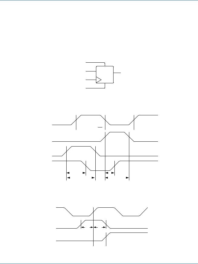
The AC Specifications are provided from 7DEOH to 7DEOH . Logic Cell diagrams and waveforms are provided from to )LJXUH .
Figure 2: EclipsePlus Logic Cell
7DEOH /RJLF &HOOV
6\PERO |
3DUDPHWHU |
9DOXH |
||
/RJLF &HOOV |
|
0LQ |
|
0D[ |
|
|
|||
|
|
|
|
|
tPD |
Combinatorial Delay of the longest path: time taken by the combinatorial circuit to |
- |
|
0.257 ns |
output |
|
|||
tSU |
Setup time: time the synchronous input of the flip-flop must be stable before the |
0.22 ns |
|
- |
active clock edge |
|
|||
tHL |
Hold time: time the synchronous input of the flip-flop must be stable after the active |
0 ns |
|
- |
clock edge |
|
|||
tCO |
Clock-to-out delay: the amount of time taken by the flip-flop to output after the |
- |
|
0.255 ns |
active clock edge. |
|
|||
tCWHI |
Clock High Time: required minimum time the clock stays high |
0.46 ns |
|
- |
tCWLO |
Clock Low Time: required minimum time that the clock stays low |
0.46 ns |
|
- |
tSET |
Set Delay: time between when the flip-flop is ”set” (high) |
- |
|
0.18 ns |
and when the output is consequently “set” (high) |
|
|||
W
WW ZZZ TXLFNORJLF FRP ‹ 4XLFN/RJLF &RUSRUDWLRQ
W
W
W
4/ (FOLSVH3OXV 'DWD 6KHHW 5HY $
7DEOH /RJLF &HOOV &RQWLQXHG
6\PERO |
3DUDPHWHU |
9DOXH |
||
/RJLF &HOOV |
|
0LQ |
|
0D[ |
|
|
|||
|
|
|
|
|
tRESET |
Reset Delay: time between when the flip-flop is ”reset” (low) and when the output |
- |
|
0.09 ns |
is consequently “reset” (low) |
|
|||
tSW |
Set Width: time that the SET signal remains high/low |
0.3 ns |
|
- |
tRW |
Reset Width: time that the RESET signal remains high/low |
0.3 ns |
|
- |
SET
D
Q
CLK
RESET
Figure 3: Logic Cell Flip-Flop
CLK
 tCWHI (min)
 tCWLO (min)
SET
RESET
Q
|
|
tRESET |
|
|
|
|
|
|
|
|
|
|
|
|
|
|
|
|
|
tSET |
|||||||
|
|
|
tRW |
|
|
|
|
|
|
tSW |
|
||
|
|
|
|
|
|
|
|
||||||
Figure 4: Logic Cell Flip-Flop Timings—First Waveform
CLK |
|
|
D |
tSU |
tHL |
|
Q
 tCO
tCO
Figure 5: Logic Cell Flip-Flop Timings—Second Waveform
W
‹ 4XLFN/RJLF &RUSRUDWLRQ ZZZ TXLFNORJLF FRP WW
W
W
W

4/ (FOLSVH3OXV 'DWD 6KHHW 5HY $
Quad net
Figure 6: EclipsePlus Global Clock Structure
7DEOH (FOLSVH3OXV &ORFN 'HOD\
&ORFN 6RXUFH |
3DUDPHWHUV |
&ORFN 3HUIRUPDQFH |
||
|
|
*OREDO |
|
'HGLFDWHG |
|
|
|
||
|
|
|
|
|
Logic Cells (Internal) |
Clock signal generated internally |
1.51 ns (max) |
|
|
|
|
|
|
|
Clock Pad |
Clock signal generated externally |
2.06 ns (max) |
|
1.73 ns (max) |
|
|
|
|
|
|
7DEOH (FOLSVH3OXV *OREDO &ORFN 'HOD\ |
|
|
|
|
|
|
|
|
&ORFN 6HJPHQW |
3DUDPHWHU |
|
9DOXH |
|
|
|
0LQ |
|
0D[ |
|
|
|
||
|
|
|
|
|
a |
Global clock pin delay to quad net |
- |
|
1.34 ns |
tPGCK |
|
|||
tBGCK |
Global clock tree delay |
- |
|
0.56 ns |
(quad net to flip-flop) |
|
|||
a.When using a PLL, tPGCK and tBGCK are effectively zero due to delay adjustment by Phase Locked Loop.
Programmable Clock |
Global Clock Buffer |
External Clock
|
Global Clock |
|
Clock |
|
Select |
tPGCK |
tBGCK |
Figure 7: Global Clock Structure Schematic
W
WW ZZZ TXLFNORJLF FRP ‹ 4XLFN/RJLF &RUSRUDWLRQ
W
W
W
4/ (FOLSVH3OXV 'DWD 6KHHW 5HY $
[9:0] |
RE |
WA |
|
[17:0] |
RCLK |
WD |
|
WE |
[9:0] |
RA |
|
|
[17:0] |
WCLK |
RD |
|
ASYNCRD |
QuickRAM |
Module |
Figure 8: RAM Module
7DEOH 5$0 &HOO 6\QFKURQRXV :ULWH 7LPLQJ
6\PERO |
3DUDPHWHU |
9DOXH |
|
|
|
|
|
5$0 &HOO 6\QFKURQRXV :ULWH 7LPLQJ |
0LQ |
0D[ |
|
|
|
|
|
tSWA |
WA setup time to WCLK: time the WRITE ADDRESS must be stable before the |
0.675 ns |
- |
active edge of the WRITE CLOCK |
|||
tHWA |
WA hold time to WCLK: time the WRITE ADDRESS must be stable after the active |
0ns |
- |
edge of the WRITE CLOCK |
|||
tSWD |
WD setup time to WCLK: time the WRITE DATA must be stable before the active |
0.654 ns |
- |
edge of the WRITE CLOCK |
|||
tHWD |
WD hold time to WCLK: time the WRITE DATA must be stable after the active edge |
0 ns |
- |
of the WRITE CLOCK |
|||
tSWE |
WE setup time to WCLK: time the WRITE ENABLE must be stable before the active |
0.623 ns |
- |
edge of the WRITE CLOCK |
|||
tHWE |
WE hold time to WCLK: time the WRITE ENABLE must be stable after the active |
0 ns |
- |
edge of the WRITE CLOCK |
|||
tWCRD |
WCLK to RD (WA = RA): time between the active WRITE CLOCK edge and the |
- |
4.38 ns |
time when the data is available at RD |
|||
WCLK
WA
tSWA |
|
tHWA |
|
WD
 tSWD
tSWD
 tHWD
tHWD
WE
 tSWE
tSWE 
 tHWE
tHWE
RD |
old data |
new data |
 tWCRD
tWCRD
Figure 9: RAM Cell Synchronous Write Timing
W
‹ 4XLFN/RJLF &RUSRUDWLRQ ZZZ TXLFNORJLF FRP WW
W
W
W
4/ (FOLSVH3OXV 'DWD 6KHHW 5HY $
7DEOH 5$0 &HOO 6\QFKURQRXV $V\QFKURQRXV 5HDG 7LPLQJ
6\PERO |
3DUDPHWHU |
9DOXH |
|
|
|
|
|
5$0 &HOO 6\QFKURQRXV 5HDG 7LPLQJ |
0LQ |
0D[ |
|
|
|
|
|
tSRA |
RA setup time to RCLK: time the READ ADDRESS must be stable before the active |
0.686 ns |
- |
edge of the READ CLOCK |
|||
tHRA |
RA hold time to RCLK: time the READ ADDRESS must be stable after the active |
0 ns |
- |
edge of the READ CLOCK |
|||
tSRE |
RE setup time to WCLK: time the READ ENABLE must be stable before the active |
0.243 ns |
- |
edge of the READ CLOCK |
|||
tHRE |
RE hold time to WCLK: time the READ ENABLE must be stable after the active |
0 ns |
- |
edge of the READ CLOCK |
|||
tRCRD |
RCLK to RD: time between the active READ CLOCK edge and the time when the |
- |
4.38 ns |
data is available at RD |
|||
5$0 &HOO $V\QFKURQRXV 5HDG 7LPLQJ |
|
|
|
|
|
|
|
rPDRD |
RA to RD: time between when the READ ADDRESS is input and when the DATA |
- |
2.06 ns |
is output |
|||
RCLK
RA
|
tSRA |
tHRA |
RE |
|
|
|
tSRE |
tHRE |
RD |
old data |
new data |
tRCRD
rPDRD
Figure 10: RAM Cell Synchronous & Asynchronous Read Timing
W
WW ZZZ TXLFNORJLF FRP ‹ 4XLFN/RJLF &RUSRUDWLRQ
W
W
W
4/ (FOLSVH3OXV 'DWD 6KHHW 5HY $
|
+ |
|
- |
INPUT |
Q E |
REGISTER |
D |
|
R |
|
PAD |
OUTPUT |
Q |
D |
|
REGISTER |
R |
|
|
OUTPUT ENABLE |
E Q |
D |
|
REGISTER |
R |
|
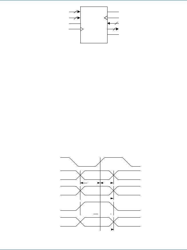
Figure 11: EclipsePlus Cell I/O
tISU
+
-
tSID
Q E
D
R
PAD
Figure 12: EclipsePlus Input Register Cell
W
‹ 4XLFN/RJLF &RUSRUDWLRQ ZZZ TXLFNORJLF FRP WW
W
W
W
4/ (FOLSVH3OXV 'DWD 6KHHW 5HY $
7DEOH ,QSXW 5HJLVWHU &HOO
6\PERO |
3DUDPHWHU |
9DOXH |
|
|
|
|
|
,QSXW 5HJLVWHU &HOO 2QO\ |
0LQ |
0D[ |
|
|
|
|
|
tISU |
Input register setup time: time the synchronous input of the flip-flop must be stable |
3.12 ns |
- |
before the active clock edge |
|||
tIHL |
Input register hold time: time the synchronous input of the flip-flop must be stable |
0 ns |
- |
after the active clock edge |
|||
tICO |
Input register clock-to-out: time taken by the flip-flop to output after the active clock |
- |
1.08 ns |
edge |
|||
tIRST |
Input register reset delay: time between when the flip-flop is “reset”(low) and when |
- |
0.99 ns |
the output is consequently “reset” (low) |
|||
tIESU |
Input register clock enable setup time: time “enable” must be stable before the |
0.37 ns |
- |
active clock edge |
|||
tIEH |
Input register clock enable hold time: time “enable” must be stable after the active |
0 ns |
- |
clock edge |
|||
7DEOH 6WDQGDUG ,QSXW 'HOD\V
6\PERO |
3DUDPHWHU |
9DOXH |
||
6WDQGDUG ,QSXW 'HOD\V |
7R JHW WKH WRWDO LQSXW GHOD\ DGG WKLV GHOD\ WR W,68 |
0LQ |
|
0D[ |
|
||||
|
|
|
|
|
tSID (LVTTL) |
LVTTL input delay: Low Voltage TTL for 3.3 V applications |
- |
|
0.34 ns |
tSID (LVCMOS2) |
LVCMOS2 input delay: Low Voltage CMOS for 2.5 V and lower |
- |
|
0.42 ns |
applications |
|
|||
|
|
|
|
|
tSID (GTL+) |
GTL+ input delay: Gunning Transceiver Logic |
- |
|
0.68 ns |
tSID (SSTL3) |
SSTL3 input delay: Stub Series Terminated Logic for 3.3 V |
- |
|
0.55 ns |
tSID (SSTL2) |
SSTL2 input delay: Stub Series Terminated Logic for 2.5 V |
- |
|
0.61 ns |
R
CLK
D
 tISU
tISU  t IHL
t IHL 
Q |
tICO |
tIRST
E
tIESU tIEH
Figure 13: EclipsePlus Input Register Cell Timing
W
WW ZZZ TXLFNORJLF FRP ‹ 4XLFN/RJLF &RUSRUDWLRQ
W
W
W
4/ (FOLSVH3OXV 'DWD 6KHHW 5HY $
PAD
OUTPUT
REGISTER
Figure 14: EclipsePlus Output Register Cell
7DEOH (FOLSVH3OXV 2XWSXW 5HJLVWHU &HOO
6\PERO |
3DUDPHWHU |
|
9DOXH |
|
|
|
|
2XWSXW 5HJLVWHU &HOO 2QO\ |
0LQ |
0D[ |
|
|
|
|
|
tOUTLH |
Output Delay low to high (90% of H) |
- |
0.40 ns |
tOUTHL |
Output Delay high to low (10% of L) |
- |
0.55 ns |
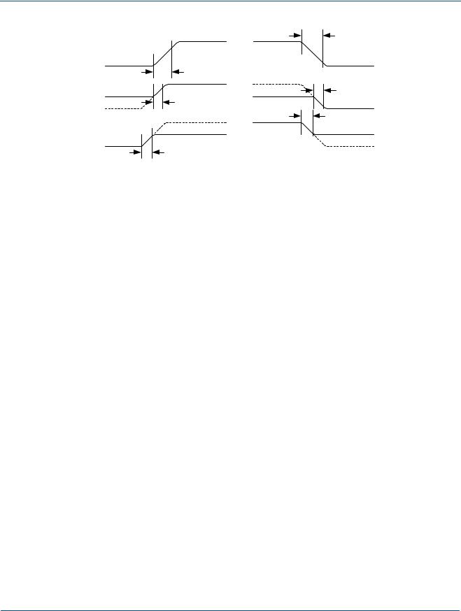
tPZH |
Output Delay tri-state to high (90% of H) |
- |
2.94 ns |
tPZL |
Output Delay tri-state to low (10% of L) |
- |
2.34 ns |
tPHZ |
Output Delay high to tri-State |
- |
3.07 ns |
tPLZ |
Output Delay low to tri-State |
- |
2.53 ns |
tCOP |
Clock-to-out delay (does not include clock tree delays) |
- |
3.15 ns (fast slew) |
10.2 ns (slow slew) |
|||
W
‹ 4XLFN/RJLF &RUSRUDWLRQ ZZZ TXLFNORJLF FRP WW
W
W
W
4/ (FOLSVH3OXV 'DWD 6KHHW 5HY $
H |
|
tOUTHL |
|
|
H |
||
L |
tOUTLH |
L |
|
|
|
||
H |
|
H |
|
Z |
|
tPZL |
|
tPZH |
Z |
||
L |
L |
||
|
|||
H |
|
tPHZ |
|
|
H |
||
Z |
|
Z |
|
L |
tPLZ |
L |
|
|
|
Figure 15: EclipsePlus Output Register Cell Timing
7DEOH 2XWSXW 6OHZ 5DWHV # 9&&,2 9
|
)DVW 6OHZ |
|
6ORZ 6OHZ |
|
|
|
|
Rising Edge |
2.8 V/ns |
|
1.0 V/ns |
|
|
|
|
Falling Edge |
2.86 V/ns |
|
1.0 V/ns |
|
|
|
|
|
7DEOH 2XWSXW 6OHZ 5DWHV # 9&&,2 9 |
|
|
|
|
|
|
|
)DVW 6OHZ |
|
6ORZ 6OHZ |
|
|
|
|
Rising Edge |
1.7 V/ns |
|
0.6 V/ns |
|
|
|
|
Falling Edge |
1.9 V/ns |
|
0.6 V/ns |
|
|
|
|
W
WW ZZZ TXLFNORJLF FRP ‹ 4XLFN/RJLF &RUSRUDWLRQ
W
W
W
4/ (FOLSVH3OXV 'DWD 6KHHW 5HY $
'& &KDUDFWHULVWLFV
The DC Specifications are provided in 7DEOH through 7DEOH .
7DEOH $EVROXWH 0D[LPXP 5DWLQJV
|
3DUDPHWHU |
|
|
9DOXH |
|
|
|
|
3DUDPHWHU |
|
|
|
|
9DOXH |
|
|
|||
|
|
|
|
|
|
|
|
|
|
|
|
|
|
|
|
|
|
||
|
9&& 9ROWDJH |
|
|
-0.5 V to 3.6 V |
|
|
|
'& ,QSXW &XUUHQW |
|
|
±20 mA |
|
|
||||||
|
|
|
|
|
|
|
|
|
|
|
|
|
|
|
|
|
|
||
|
9&&,2 9ROWDJH |
|
|
-0.5 V to 4.6 V |
|
|
|
(6' 3DG 3URWHFWLRQ |
|
|
±2000 V |
|
|
||||||
|
|
|
|
|
|
|
|
|
|
|
|
|
|
|
|
|
|
||
|
,15() 9ROWDJH |
|
|
2.7 V |
|
|
|
/HDGHG 3DFNDJH |
-65° C to + 150° C |
||||||||||
|
|
|
|
|
|
6WRUDJH 7HPSHUDWXUH |
|||||||||||||
|
|
|
|
|
|
|
|
|
|
|
|
|
|
||||||
|
|
|
|
|
|
|
|
|
|
|
|
|
|
|
|
|
|
||
|
,QSXW 9ROWDJH |
|
-0.5 V to VCCIO +0.5 V |
|
|
/DPLQDWH 3DFNDJH %*$ |
-55° C to + 125° C |
||||||||||||
|
/DWFK XS ,PPXQLW\ |
|
|
±100 mA |
|
|
|
6WRUDJH 7HPSHUDWXUH |
|||||||||||
|
|
|
|
|
|
|
|
|
|
|
|||||||||
|
|
|
|
|
|
|
|
|
|
|
|
|
|
|
|
|
|||
|
|
|
|
|
|
|
|
|
|
|
|
|
|
|
|
|
|
||
|
|
|
|
|
7DEOH 2SHUDWLQJ 5DQJH |
|
|
|
|
|
|
|
|||||||
|
|
|
|
|
|
|
|
|
|
|
|
|
|
|
|
||||
|
6\PERO |
|
3DUDPHWHU |
0LOLWDU\ |
|
,QGXVWULDO |
|
&RPPHUFLDO |
8QLW |
|
|||||||||
|
|
|
|
|
|
0LQ |
|
0D[ |
|
0LQ |
|
0D[ |
|
0LQ |
|
0D[ |
|
|
|
|
|
|
|
|
|
|
|
|
|
|
|
|
|||||||
|
|
|
|
|
|
|
|
|
|
|
|
|
|
|
|
|
|
|
|
|
VCC |
Supply Voltage |
2.3 |
|
2.7 |
|
2.3 |
|
2.7 |
|
2.3 |
|
2.7 |
V |
|||||
|
VCCIO |
I/O Input Tolerance Voltage |
2.3 |
|
3.6 |
|
2.3 |
|
3.6 |
|
2.3 |
|
3.6 |
V |
|
||||
|
TA |
Ambient Temperature |
-55 |
|
|
|
-40 |
|
85 |
|
0 |
|
70 |
°C |
|||||
|
|
|
|
|
|
|
|
|
|
|
|
|
|
|
|
|
|
||
|
TC |
Case Temperature |
- |
|
|
125 |
|
- |
|
- |
|
- |
|
- |
°C |
|
|||
|
|
|
|
|
|
|
|
|
|
|
|
|
|
|
|
|
|
|
|
|
|
|
|
|
-4 Speed Grade |
0.42 |
|
2.3 |
|
0.43 |
|
2.16 |
|
0.47 |
|
2.11 |
n/a |
||
|
|
|
|
|
|
|
|
|
|
|
|
|
|
|
|
|
|
|
|
|
K |
Delay Factor |
-5 Speed Grade |
0.42 |
|
1.92 |
|
0.43 |
|
1.80 |
|
0.46 |
|
1.76 |
n/a |
|
|||
|
|
|
|
|
|
|
|
|
|
|
|
|
|
|
|
||||
|
-6 Speed Grade |
0.42 |
|
1.35 |
|
0.43 |
|
1.26 |
|
0.46 |
|
1.23 |
n/a |
||||||
|
|
|
|
|
|
|
|
|
|
||||||||||
|
|
|
|
|
|
|
|
|
|
|
|
|
|
|
|
|
|
|
|
|
|
|
|
|
-7 Speed Grade |
0.42 |
|
1.27 |
|
0.43 |
|
1.19 |
|
0.46 |
|
1.16 |
n/a |
|
|
|
|
|
|
|
|
|
|
|
|
|
|
|
|
|
|
|
|
|
|
7DEOH '& &KDUDFWHULVWLFV
6\PERO |
3DUDPHWHU |
&RQGLWLRQV |
0LQ |
0D[ |
8QLWV |
|||
|
|
|
|
|
|
|
||
|
II |
I or I/O Input Leakage Current |
VI = VCCIO or GND |
-10 |
10 |
µA |
||
IOZ |
3-State Output Leakage Current |
VI = VCCIO or GND |
-10 |
10 |
µA |
|||
CI |
Input Capacitancea |
|
- |
|
- |
8 |
pF |
|
I |
Output Short Circuit Currentb |
Vo = GND |
-15 |
-180 |
mA |
|||
|
OS |
|
Vo = VCC |
40 |
210 |
mA |
||
|
|
|
||||||
I |
CC |
D.C. Supply Currentc |
V V = V |
CCIO |
or GND |
0.50 (typ) |
2 |
mA |
|
|
I, o |
|
|
|
|
||
ICCIO |
D.C. Supply Current on VCCIO |
|
- |
|
0 |
2 |
mA |
|
ICCIO(DIF) |
D.C. Supply Current on VCCIO |
|
- |
|
- |
- |
mA |
|
for Differential I/O |
|
|
||||||
|
|
|
|
|
|
|
|
|
IREF |
D.C. Supply Current on INREF |
|
- |
|
-10 |
10 |
µA |
|
IPD |
Pad Pull-down (programmable) |
VCCIO = 3.6 V |
- |
150 |
µA |
|||
D &DSDFLWDQFH LV VDPSOH WHVWHG RQO\ &ORFN SLQV DUH S) PD[LPXP
E 2QO\ RQH RXWSXW DW D WLPH 'XUDWLRQ VKRXOG QRW H[FHHG VHFRQGV
F )RU FRPPHUFLDO JUDGH GHYLFHV RQO\ 0D[LPXP ,&& LV P$ IRU FRPPHUFLDO
JUDGH DQG DOO LQGXVWULDO JUDGH GHYLFHV DQG P$ IRU DOO PLOLWDU\ JUDGH GHYLFHV
W
‹ 4XLFN/RJLF &RUSRUDWLRQ ZZZ TXLFNORJLF FRP WW
W
W
W
4/ (FOLSVH3OXV 'DWD 6KHHW 5HY $
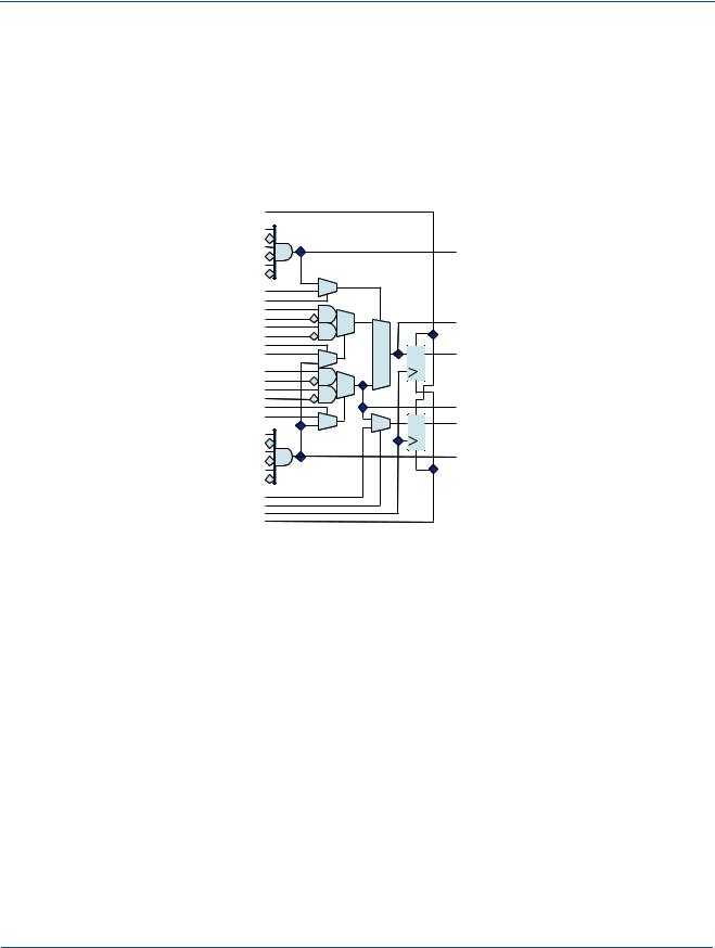
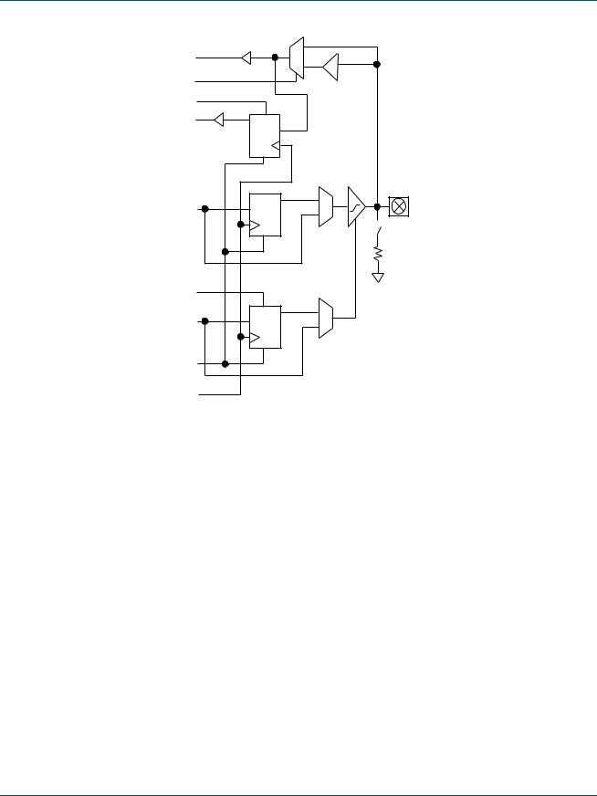
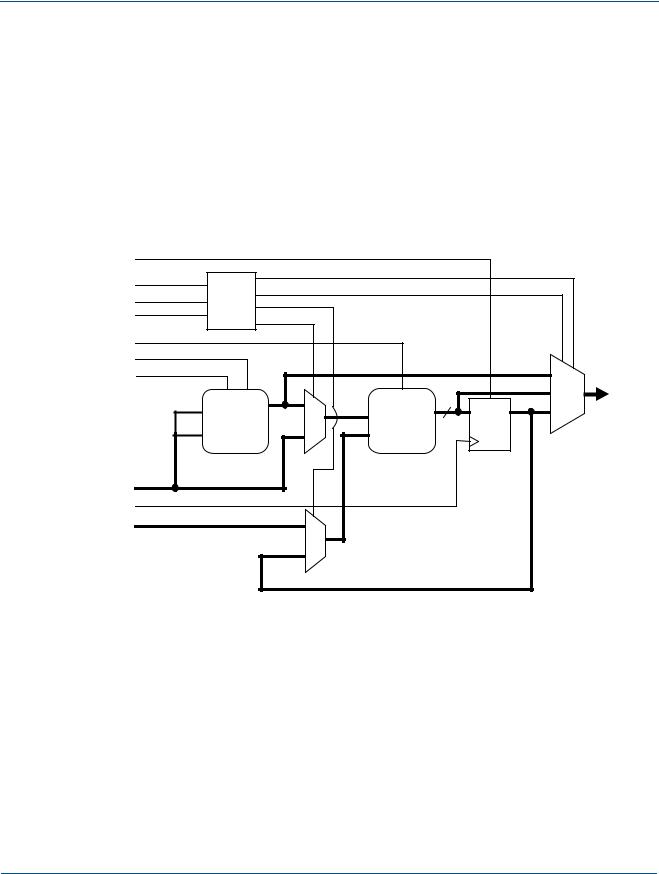
(PEHGGHG &RPSXWDWLRQDO 8QLW (&8
Traditional Programmable Logic architectures do not implement arithmetic functions efficiently or effectively—these functions require high logic cell usage while garnering only moderate performance results.
The QL7180 architecture allows for functionality above and beyond that achievable using programmable logic devices. By embedding a dynamically reconfigurable computational unit, the QL7180 device can address various arithmetic functions efficiently.
This approach offers greater performance than traditional programmable logic implementations. The embedded block is implemented at the transistor level as shown in
)LJXUH .
RESET |
|
|
D |
|
|
|
|
|
|
|
|
|
|
|
|
|
|
|
|
S1 |
|
3-4 |
C |
|
|
|
|
|
|
S2 |
|
B |
|
|
|
|
|
|
|
|
decoder |
|
|
|
|
|
|
||
S3 |
|
A |
|
|
|
|
|
|
|
|
|
|
|
|
|
|
|
||
CIN |
|
|
|
|
|
|
|
|
|
SIGN1 |
|
|
|
|
|
|
|
|
|
SIGN2 |
|
|
|
|
|
|
|
00 |
Q[0:16] |
|
|
|
|
|
|
|
|
|
|
|
|
|
|
|
|
|
|
01 |
3-1 |
|
|
|
|
|
|
|
|
|
mux |
|
A[0:7] |
8-bit |
2-1 |
16-bit |
|
D |
Q |
10 |
|
|
|
17 inc. |
17-bit |
|
|
||||
|
|
Multiplier |
mux |
Adder |
|
|
|||
|
A[8:15] |
COUT Register |
|
|
|||||
|
|
|
|
|
|
||||
A[0:15] |
|
|
|
|
|
|
|
|
|
CLK |
|
|
|
|
|
|
|
|
|
B[0:15] |
|
|
2-1 |
|
|
|
|
|
|
|
|
|
|
|
|
|
|
|
|
|
|
|
mux |
|
|
|
|
|
|
Figure 16: ECU Block Diagram
The 18 QL7180 ECU blocks are placed next to the SRAM circuitry for efficient memory/instruction fetch and addressing for DSP algorithmic implementations.
Eighteen 8-bit MAC functions can be implemented per cycle for a total of 1.8 billion MACs when clocked at 100 MHz. Additional multiply-accumulate functions can be implemented in the programmable logic.
The modes for the ECU block are dynamically re-programmable through the programmable logic.
W
WW ZZZ TXLFNORJLF FRP ‹ 4XLFN/RJLF &RUSRUDWLRQ
W
W
W

4/ (FOLSVH3OXV 'DWD 6KHHW 5HY $
7DEOH (&8 0RGH 6HOHFW &ULWHULD
,QVWUXFWLRQ |
2SHUDWLRQ |
(&8 3HUIRUPDQFHD:&&E |
|||||
6 |
6 |
6 |
W3' |
W68 |
W&2 |
||
|
|||||||
0 |
0 |
0 |
Multiply |
6.57 ns |
|
|
|
max |
|
|
|||||
|
|
|
|
|
|
||
|
|
|
|
|
|
|
|
0 |
0 |
1 |
Multiply-Add |
8.84 ns |
|
|
|
max |
|
|
|||||
|
|
|
|
|
|
||
|
|
|
|
|
|
|
|
0 |
1 |
0 |
Accumulatec |
|
3.91 ns |
1.16 ns |
|
|
min |
max |
|||||
|
|
|
|
|
|||
|
|
|
|
|
|
|
|
0 |
1 |
1 |
Add |
3.14 ns |
|
|
|
max |
|
|
|||||
|
|
|
|
|
|
||
|
|
|
|
|
|
|
|
1 |
0 |
0 |
Multiply (registered)d |
|
9.61 ns |
1.16 ns |
|
|
min |
max |
|||||
|
|
|
|
|
|||
|
|
|
|
|
|
|
|
1 |
0 |
1 |
MultiplyAdd (registered) |
|
9.61 ns |
1.16 ns |
|
|
min |
max |
|||||
|
|
|
|
|
|||
|
|
|
|
|
|
|
|
1 |
1 |
0 |
Multiply - Accumulate |
|
9.61 ns |
1.16 ns |
|
|
min |
max |
|||||
|
|
|
|
|
|||
|
|
|
|
|
|
|
|
1 |
1 |
1 |
Add (registered) |
|
3.91 ns |
1.16 ns |
|
|
min |
max |
|||||
|
|
|
|
|
|||
|
|
|
|
|
|
|
|
D WPD WSU DQG WCO GR QRW LQFOXGH URXWLQJ SDWKV LQ RXW RI WKH (&8 EORFN
E 7LPLQJ QXPEHUV UHSUHVHQW :RUVW &DVH &RPPHUFLDO FRQGLWLRQV
F ,QWHUQDO IHHGEDFN SDWK LQ (&8 UHVWULFWV PD[ FON IUHTXHQF\ WR 0+]
G % > @ VHW WR ]HUR
W
‹ 4XLFN/RJLF &RUSRUDWLRQ ZZZ TXLFNORJLF FRP WW
W
W
W
4/ (FOLSVH3OXV 'DWD 6KHHW 5HY $
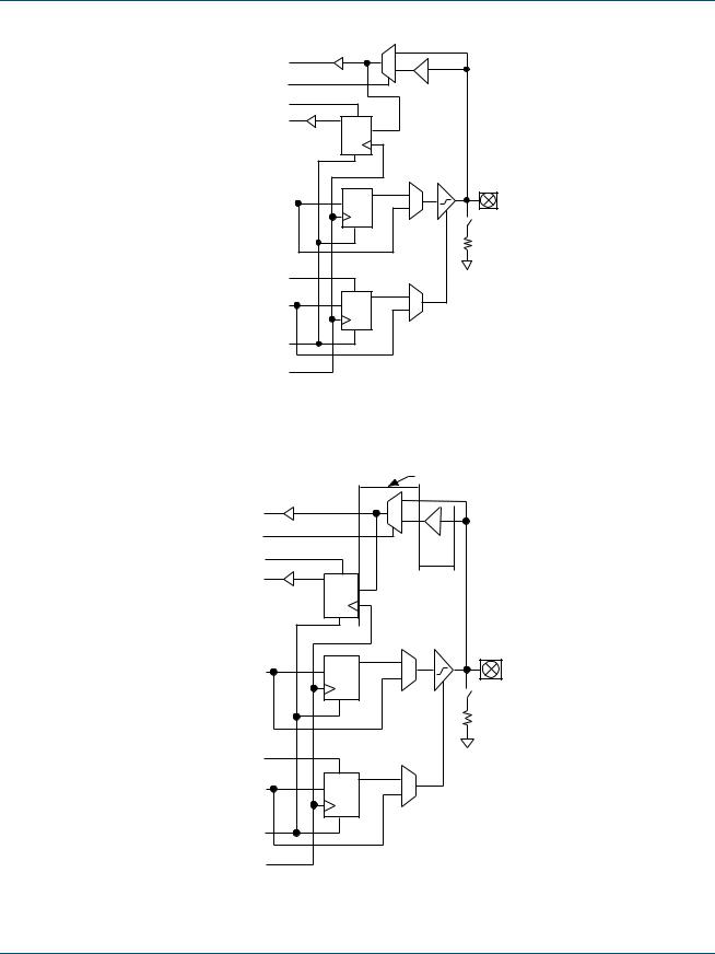
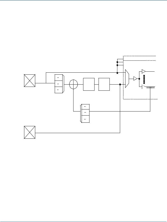
3KDVH /RFNHG /RRSV 3//V
Instead of requiring extra components, designers simply need to instantiate one of the preconfigured models (described in this section). The QuickLogic built-in PLLs support a wider range of frequencies than many other PLLs. Also, QuickLogic PLLs can be cascaded to support different ranges of frequency multiplications or divisions, driving the device at a faster or slower rate than the incoming clock frequency. Most importantly, they achieve a very short clock-to-out time—generally less than 3 ns. This low clock-to-out time is achieved by the PLL subtracting the clock tree delay through the feedback path, effectively making the clock tree delay zero.
)LJXUH illustrates a typical QuickLogic ESP PLL.
1st Quadrant
2nd Quadrant 3rd Quadrant
FIN |
Frequency Divide |
PLL Bypass |
4th Quadrant |
|
|||
|
|
|
. |
|
|
Clock |
.1 |
|
|
|
|
|
|
Tree |
. |
+ |
Filter |
vco |
.2 |
|||
. |
|
- |
|
.4 |
|
|
Frequency Multiply
.
.1
.
.2
.
.4
FOUT
Figure 17: PLL Block
Fin represents a very stable high-frequency input clock and produces an accurate signal reference. This signal can either bypass the PLL entirely, thus entering the clock tree directly, or it can pass through the PLL itself.
Within the PLL, a voltage-controlled oscillator (VCO) is added to the circuit. The external Fin signal and the local VCO form a control loop. The VCO is multiplied or divided down to the reference frequency, so that a phase detector (the crossed circle in )LJXUH ) can compare the two signals. If the phases of the external and local signals are not within the tolerance required, the phase detector sends a signal through the charge pump and loop filter ()LJXUH ). The charge pump generates an error voltage to bring the VCO back into alignment and the loop filter removes any high frequency noise before the error voltage enters the VCO. This new VCO signal enters the clock tree to drive the chip's circuitry.
W
WW ZZZ TXLFNORJLF FRP ‹ 4XLFN/RJLF &RUSRUDWLRQ
W
W
W
 Loading...