


QUICK LOGIC QL7100-4PS484C, QL7100-4PS484I, QL7100-4PS484M, QL7100-4PT208C, QL7100-4PT208I Datasheet
...4/ (FOLSVH3OXV 'DWD 6KHHW
W W W W W W &RPELQLQJ 3HUIRUPDQFH 'HQVLW\ DQG (PEHGGHG 5$0
'HYLFH +LJKOLJKWV
)OH[LEOH 3URJUDPPDEOH /RJLF
‡.25 m five layer metal CMOS Process
‡2.5 V VCC, 2.5/3.3 V Drive Capable I/O
‡960 Logic Cells
‡248,160 Max System Gates
‡Up to 250 I/O Pins
(PEHGGHG 'XDO 3RUW 65$0
‡Twenty 2,304-bit Dual Port High Performance SRAM Blocks
‡46,100 RAM bits
‡RAM/ROM/FIFO Wizard for Automatic Configuration
‡Configurable and Cascadable
3URJUDPPDEOH , 2
‡High performance Enhanced I/O (EIO)— less than 3 ns Tco
‡Programmable Slew Rate Control
‡Programmable I/O Standards:
‡LVTTL, LVCMOS, PCI, GTL+, SSTL2, and SSTL3
‡Eight Independent I/O Banks
‡Three Register Configurations: Input, Output, and Output Enable
$GYDQFHG &ORFN 1HWZRUN
‡Nine Global Clock Networks:
‡One Dedicated
‡Eight Programmable
‡20 Quad-Net Networks—five per Quadrant
‡16 I/O Controls—two per I/O Bank
‡Four phase locked loops
(PEHGGHG &RPSXWDWLRQDO 8QLWV
ECUs provide integrated Multiply, Add, and Accumulate Functions.
|
PLL |
|
|
|
Memory - Dual Port RAM |
PLL |
|
|||||||||||||||||||||||
|
|
|
|
|
||||||||||||||||||||||||||
|
|
Embedded Computational Units |
|
|
||||||||||||||||||||||||||
|
|
|
|
|
|
|
|
|
|
|
|
|
|
|
|
|
|
|
|
|
|
|
|
|
|
|
|
|
|
|
|
|
|
|
|
|
|
|
|
|
|
|
|
|
|
|
|
|
|
|
|
|
|
|
|
|
|
|
|
|
|
|
|
|
|
|
|
|
|
|
|
|
|
|
|
|
|
|
|
|
|
|
|
|
|
|
|
|
|
|
|
|
|
|
|
|
|
|
|
|
|
|
|
|
|
|
|
|
|
|
|
|
|
|
|
|
|
|
|
|
|
|
|
 High Speed Logic Cells
248K Gates
|
|
|
|
|
|
|
|
|
|
|
|
|
|
|
|
|
|
|
|
|
|
|
|
|
|
|
|
|
|
|
|
|
|
|
|
|
|
|
|
|
|
|
|
|
|
|
|
|
|
|
|
|
|
|
|
|
|
|
|
|
|
|
PLL |
|
|
|
Memory - Dual Port RAM |
PLL |
|
|||||||||||||||||||||||
|
|
|
|
|
|
|
|
|
|
|
|
|
|
|
|
|
|
|
|
|
|
|
|
|
|
|
|
|
|
|
|
|
|
|
|
|
|
|
|
|
|
|
|
|
|
|
|
|
|
|
|
|
|
|
|
|
|
|
|
|
|
)LJXUH (FOLSVH3OXV %ORFN 'LDJUDP
W
‹ 4XLFN/RJLF &RUSRUDWLRQ ZZZ TXLFNORJLF FRP WW
W
W
W

4/ (FOLSVH3OXV 'DWD 6KHHW 5HY $
(OHFWULFDO 6SHFLILFDWLRQV
$& &KDUDFWHULVWLFV
*(at VCC = 2.5 V, TA = 25° C, Typical Corner, Speed Grade = -7 (K = 0.74))
The AC Specifications are provided from 7DEOH to 7DEOH . Logic Cell diagrams and waveforms are provided from to )LJXUH .
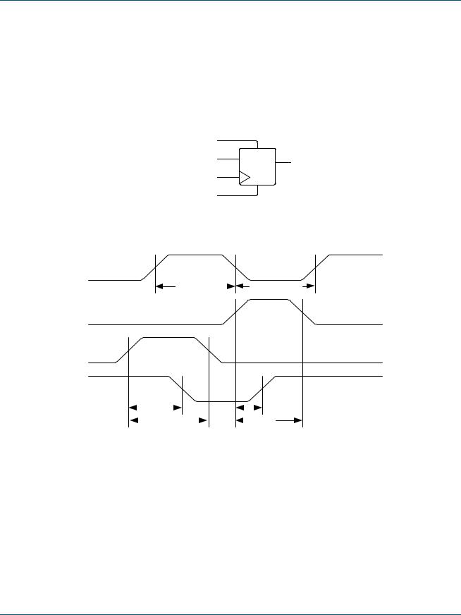
)LJXUH (FOLSVH3OXV /RJLF &HOO
7DEOH /RJLF &HOOV
|
|
6\PERO |
3DUDPHWHU |
9DOXH |
|
||
|
|
/RJLF &HOOV |
|
0LQ |
|
0D[ |
|
|
|
|
|
|
|||
|
|
|
|
|
|
|
|
|
|
tPD |
Combinatorial Delay of the longest path: time taken by the combinatorial circuit to |
- |
|
0.257 ns |
|
|
|
output |
|
||||
|
|
tSU |
Setup time: time the synchronous input of the flip-flop must be stable before the |
0.22 ns |
|
- |
|
|
|
active clock edge |
|
|
|||
|
|
tHL |
Hold time: time the synchronous input of the flip-flop must be stable after the active |
0 ns |
|
- |
|
|
|
clock edge |
|
|
|||
|
|
tCO |
Clock-to-out delay: the amount of time taken by the flip-flop to output after the |
- |
|
0.255 ns |
|
|
|
active clock edge. |
|
|
|||
|
|
tCWHI |
Clock High Time: required minimum time the clock stays high |
0.46 ns |
|
- |
|
|
|
tCWLO |
Clock Low Time: required minimum time that the clock stays low |
0.46 ns |
|
- |
|
|
|
tSET |
Set Delay: time between when the flip-flop is ”set” (high) |
- |
|
0.18 ns |
|
|
|
and when the output is consequently “set” (high) |
|
||||
|
|
|
|
|
|
|
|
W |
|
|
|
|
|
||
WW ZZZ TXLFNORJLF FRP |
|
‹ 4XLFN/RJLF &RUSRUDWLRQ |
|||||
W |
|
|
|
|
|
||
W |
|
|
|
|
|
||
W |
|
|
|
|
|
||
4/ (FOLSVH3OXV 'DWD 6KHHW 5HY $
7DEOH /RJLF &HOOV &RQWLQXHG
6\PERO |
3DUDPHWHU |
9DOXH |
||
/RJLF &HOOV |
|
0LQ |
|
0D[ |
|
|
|||
|
|
|
|
|
tRESET |
Reset Delay: time between when the flip-flop is ”reset” (low) and when the output |
- |
|
0.09 ns |
is consequently “reset” (low) |
|
|||
tSW |
Set Width: time that the SET signal remains high/low |
0.3 ns |
|
- |
tRW |
Reset Width: time that the RESET signal remains high/low |
0.3 ns |
|
- |
SET
D
Q
CLK
RESET
)LJXUH /RJLF &HOO )OLS )ORS
CLK
tCWHI (min) |
|
tCWLO (min) |
|
SET
RESET
Q
|
|
tRESET |
|
|
|
|
|
|
|
|
|
|
|
|
|
|
|
|
tSET |
||||||
|
|
|
tRW |
|
|
|
|
|
tSW |
|||
|
|
|
|
|
|
|
||||||
)LJXUH /RJLF &HOO )OLS )ORS 7LPLQJV²)LUVW :DYHIRUP
W
‹ 4XLFN/RJLF &RUSRUDWLRQ ZZZ TXLFNORJLF FRP WW
W
W
W

4/ (FOLSVH3OXV 'DWD 6KHHW 5HY $
CLK |
|
|
D |
tSU |
tHL |
|
Q
tCO
)LJXUH /RJLF &HOO )OLS )ORS 7LPLQJV²6HFRQG :DYHIRUP
Quad net
)LJXUH (FOLSVH3OXV *OREDO &ORFN 6WUXFWXUH
0
7DEOH (FOLSVH3OXV &ORFN 'HOD\
|
|
&ORFN 6RXUFH |
3DUDPHWHUV |
&ORFN 3HUIRUPDQFH |
|
||
|
|
|
|
*OREDO |
|
'HGLFDWHG |
|
|
|
|
|
|
|
||
|
|
|
|
|
|
|
|
|
|
Logic Cells (Internal) |
Clock signal generated internally |
1.51 ns (max) |
|
|
|
|
|
|
|
|
|
|
|
|
|
Clock Pad |
Clock signal generated externally |
2.06 ns (max) |
|
1.73 ns (max) |
|
|
|
|
|
|
|
|
|
|
|
|
7DEOH (FOLSVH3OXV *OREDO &ORFN 'HOD\ |
|
|
|
|
|
|
|
|
|
|
|
|
|
|
&ORFN 6HJPHQW |
3DUDPHWHU |
|
9DOXH |
|
|
|
|
|
|
0LQ |
|
0D[ |
|
|
|
|
|
|
|
||
|
|
|
|
|
|
|
|
|
|
a |
Global clock pin delay to quad net |
- |
|
1.34 ns |
|
|
|
tPGCK |
|
||||
|
|
tBGCK |
Global clock tree delay (quad net to |
- |
|
0.56 ns |
|
|
|
flip-flop) |
|
|
|||
|
|
|
|
|
|
|
|
W |
|
|
|
|
|
||
WW ZZZ TXLFNORJLF FRP |
|
|
|
‹ 4XLFN/RJLF &RUSRUDWLRQ |
|||
W |
|
|
|
|
|
||
W |
|
|
|
|
|
||
W |
|
|
|
|
|
||
4/ (FOLSVH3OXV 'DWD 6KHHW 5HY $
D :KHQ XVLQJ D 3// W3*&. DQG W%*&. DUH HIIHFWLYHO\ ]HUR GXH WR GHOD\ DGMXVWPHQW E\ 3KDVH
/RFNHG /RRS
Programmable Clock
External Clock
tPGCK
Global Clock Buffer

 Global Clock
Clock
Select
tBGCK
)LJXUH *OREDO &ORFN 6WUXFWXUH 6FKHPDWLF |
|
||
[9:0] |
|
|
|
WA |
|
RE |
|
[17:0] |
|
RCLK |
|
WD |
|
|
|
|
|
[9:0] |
|
WE |
|
RA |
|
|
|
[17:0] |
|
WCLK |
RD |
|
|
|
|
ASYNCRD |
|
|
RAM Module |
|
|
)LJXUH 5$0 0RGXOH |
|
||
7DEOH 5$0 &HOO 6\QFKURQRXV :ULWH 7LPLQJ |
|
||
6\PERO |
3DUDPHWHU |
9DOXH |
|
|
|||
|
|
0LQ |
0D[ |
tSWA |
WA setup time to WCLK: time the WRITE ADDRESS must be stable before the |
0.675 ns |
- |
active edge of the WRITE CLOCK |
|||
tHWA |
WA hold time to WCLK: time the WRITE ADDRESS must be stable after the active |
0 ns |
- |
edge of the WRITE CLOCK |
|||
tSWD |
WD setup time to WCLK: time the WRITE DATA must be stable before the active |
0.654 ns |
- |
edge of the WRITE CLOCK |
|||
tHWD |
WD hold time to WCLK: time the WRITE DATA must be stable after the active edge |
0 ns |
- |
of the WRITE CLOCK |
|||
tSWE |
WE setup time to WCLK: time the WRITE ENABLE must be stable before the active |
0.623 ns |
- |
edge of the WRITE CLOCK |
|||
tHWE |
WE hold time to WCLK: time the WRITE ENABLE must be stable after the active |
0 ns |
- |
edge of the WRITE CLOCK |
|||
tWCRD |
WCLK to RD (WA = RA): time between the active WRITE CLOCK edge and the |
- |
4.38 ns |
time when the data is available at RD |
W
‹ 4XLFN/RJLF &RUSRUDWLRQ ZZZ TXLFNORJLF FRP WW
W
W
W
4/ (FOLSVH3OXV 'DWD 6KHHW 5HY $
|
WCLK |
|
|
|
|
|
|
|
|
|
|
|
|
|
|
|
WA |
|
|
|
|
|
|
|
|
|
|
|
|
|
|
|
|
|
|
|
|
|
|
|
|
|
|
|
|
|
|
|
WD |
|
|
tSWA |
|
|
|
|
|
tHWA |
|
|
|
|
|
|
|
|
|
|
|
|
|
|
|
|
|||||
|
|
|
|
|
|
|
|
|
|
|
|
|
|
|
|
|
WE |
|
|
tSWD |
|
|
|
tHWD |
|
|
|
|
|||
|
|
|
|
|
|
|
|
|
|||||||
|
|
|
|
|
|
|
|
|
|
|
|
|
|
|
|
|
|
|
|
tSWE |
|
|
|
tHWE |
|
|
|
|
|||
|
|
|
|
|
|
|
|
|
|||||||
|
RD |
|
|
old data |
|
|
|
new data |
|
|
|
||||
|
|
|
|
|
|
|
|
|
|
tWCRD |
|
|
|
|
|
|
|
|
|
|
|
|
|
|
|
|
|
|
|
|
|
|
)LJXUH 5$0 &HOO 6\QFKURQRXV :ULWH 7LPLQJ |
|
|
|
|||||||||||
|
7DEOH 5$0 &HOO 6\QFKURQRXV $V\QFKURQRXV 5HDG 7LPLQJ |
|
|
|
|||||||||||
|
|
|
|
|
|
|
|
|
|
|
|
|
|
|
|
6\PERO |
5$0 &HOO 6\QFKURQRXV 5HDG 7LPLQJ |
9DOXH |
|||||||||||||
|
3DUDPHWHU |
|
|
|
|
0LQ |
|
0D[ |
|||||||
|
|
|
|
|
|
||||||||||
|
|
|
|
|
|
|
|||||||||
|
|
|
|
|
|
|
|
|
|
|
|
|
|
|
|
tSRA |
RA setup time to RCLK: time the READ ADDRESS must be stable before the active |
0.686 ns |
|
- |
|||||||||||
edge of the READ CLOCK |
|
|
|
|
|
|
|
|
|
|
|
|
|||
tHRA |
RA hold time to RCLK: time the READ ADDRESS must be stable after the active |
0 ns |
|
- |
|||||||||||
edge of the READ CLOCK |
|
|
|
|
|
|
|
|
|
|
|
|
|||
tSRE |
RE setup time to WCLK: time the READ ENABLE must be stable before the active |
0.243 ns |
|
- |
|||||||||||
edge of the READ CLOCK |
|
|
|
|
|
|
|
|
|
|
|
|
|||
tHRE |
RE hold time to WCLK: time the READ ENABLE must be stable after the active |
0 ns |
|
- |
|||||||||||
edge of the READ CLOCK |
|
|
|
|
|
|
|
|
|
|
|
|
|||
tRCRD |
RCLK to RD: time between the active READ CLOCK edge and the time when the |
- |
|
4.38 ns |
|||||||||||
data is available at RD |
|
|
|
|
|
|
|
|
|
|
|
|
|||
|
5$0 &HOO $V\QFKURQRXV 5HDG 7LPLQJ |
|
|
|
|||||||||||
|
|
|
|
|
|
|
|
|
|
|
|
|
|
|
|
rPDRD |
RA to RD: time between when the READ ADDRESS is input and when the DATA |
- |
|
2.06 ns |
|||||||||||
is output |
|
|
|
|
|
|
|
|
|
|
|
|
|||
W
WW ZZZ TXLFNORJLF FRP ‹ 4XLFN/RJLF &RUSRUDWLRQ
W
W
W
4/ (FOLSVH3OXV 'DWD 6KHHW 5HY $
RCLK
RA
|
tSRA |
tHRA |
RE |
|
|
|
tSRE |
tHRE |
RD |
old data |
new data |
 tRCRD
tRCRD 
rPDRD
)LJXUH 5$0 &HOO 6\QFKURQRXV $V\QFKURQRXV 5HDG 7LPLQJ
|
+ |
|
- |
INPUT |
Q E |
REGISTER |
D |
|
R |
|
PAD |
OUTPUT |
Q |
D |
|
REGISTER |
R |
|
|
OUTPUT ENABLE |
E Q |
D |
|
REGISTER |
R |
|
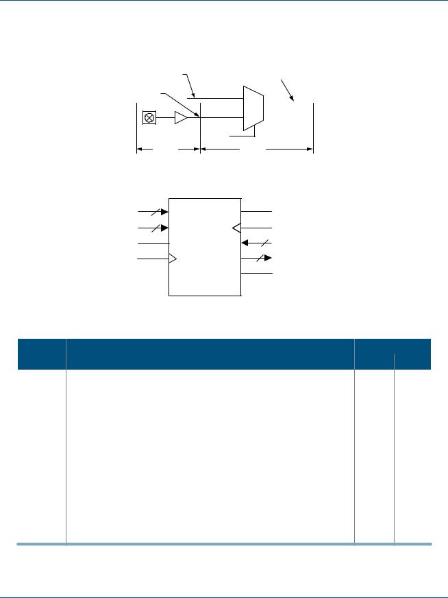
)LJXUH (FOLSVH3OXV &HOO , 2
W
‹ 4XLFN/RJLF &RUSRUDWLRQ ZZZ TXLFNORJLF FRP WW
W
W
W
4/ (FOLSVH3OXV 'DWD 6KHHW 5HY $
tISU
+
-
tSID
Q E
D
R
PAD
)LJXUH (FOLSVH3OXV ,QSXW 5HJLVWHU &HOO
7DEOH ,QSXW 5HJLVWHU &HOO
|
|
9DOXH |
||
6\PERO |
3DUDPHWHU ,QSXW 5HJLVWHU &HOO 2QO\ |
0LQ |
|
0D[ |
|
||||
|
|
|
||
|
|
|
|
|
tISU |
Input register setup time: time the synchronous input of the flip-flop must be stable |
3.12 ns |
|
- |
before the active clock edge |
|
|||
tIHL |
Input register hold time: time the synchronous input of the flip-flop must be stable |
0 ns |
|
- |
after the active clock edge |
|
|||
tICO |
Input register clock-to-out: time taken by the flip-flop to output after the active clock |
- |
|
1.08 ns |
edge |
|
|||
tIRST |
Input register reset delay: time between when the flip-flop is “reset” (low) and when |
- |
|
0.99 ns |
the output is consequently “reset” (low) |
|
|||
tIESU |
Input register clock enable setup time: time “enable” must be stable before the |
0.37 ns |
|
- |
active clock edge |
|
|||
tIEH |
Input register clock enable hold time: time “enable” must be stable after the active |
0 ns |
|
- |
clock edge |
|
|||
W
WW ZZZ TXLFNORJLF FRP ‹ 4XLFN/RJLF &RUSRUDWLRQ
W
W
W
4/ (FOLSVH3OXV 'DWD 6KHHW 5HY $
7DEOH 6WDQGDUG ,QSXW 'HOD\V
6\PERO |
3DUDPHWHU |
9DOXH |
||
6WDQGDUG ,QSXW 'HOD\V |
7R JHW WKH WRWDO LQSXW GHOD\ DGG WKLV GHOD\ WR W,68 |
0LQ |
|
0D[ |
|
||||
|
|
|
|
|
tSID (LVTTL) |
LVTTL input delay: Low Voltage TTL for 3.3 V applications |
- |
|
0.34 ns |
tSID (LVCMOS2) |
LVCMOS2 input delay: Low Voltage CMOS for 2.5 V and lower |
- |
|
0.42 ns |
applications |
|
|||
|
|
|
|
|
tSID (GTL+) |
GTL+ input delay: Gunning Transceiver Logic |
- |
|
0.68 ns |
tSID (SSTL3) |
SSTL3 input delay: Stub Series Terminated Logic for 3.3 V |
- |
|
0.55 ns |
tSID (SSTL2) |
SSTL2 input delay: Stub Series Terminated Logic for 2.5 V |
- |
|
0.61 ns |
R
CLK
D
 tISU
tISU  t IHL
t IHL 
Q |
tICO |
tIRST
E
tIESU tIEH
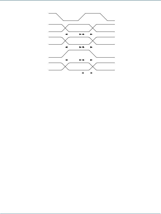
)LJXUH (FOLSVH3OXV ,QSXW 5HJLVWHU &HOO 7LPLQJ
W
‹ 4XLFN/RJLF &RUSRUDWLRQ ZZZ TXLFNORJLF FRP WW
W
W
W
4/ (FOLSVH3OXV 'DWD 6KHHW 5HY $
PAD
OUTPUT
REGISTER
)LJXUH (FOLSVH3OXV 2XWSXW 5HJLVWHU &HOO
7DEOH (FOLSVH3OXV 2XWSXW 5HJLVWHU &HOO
6\PERO |
3DUDPHWHU |
|
9DOXH |
|
|
|
|
2XWSXW 5HJLVWHU &HOO 2QO\ |
0LQ |
0D[ |
|
|
|
|
|
tOUTLH |
Output Delay low to high (90% of H) |
- |
0.40 ns |
tOUTHL |
Output Delay high to low (10% of L) |
- |
0.55 ns |
tPZH |
Output Delay tri-state to high (90% of H) |
- |
2.94 ns |
tPZL |
Output Delay tri-state to low (10% of L) |
- |
2.34 ns |
tPHZ |
Output Delay high to tri-State |
- |
3.07 ns |
tPLZ |
Output Delay low to tri-State |
- |
2.53 ns |
tCOP |
Clock-to-out delay (does not include clock tree delays) |
- |
3.15 ns (fast slew) |
10.2 ns (slow slew) |
|||
W
WW ZZZ TXLFNORJLF FRP ‹ 4XLFN/RJLF &RUSRUDWLRQ
W
W
W
4/ (FOLSVH3OXV 'DWD 6KHHW 5HY $
H |
|
|
|
|
|
|
|
|
|
|
|
|
|
|
|
|
|
|
|
|
|
|
|
|
|
|
|
tOUTHL |
|
|
|
|
|
|
|
|
|
|
|
|
|
H |
|
|
|
|
|
|
|||||||||
|
|
|
|
|
|
|
|
|
|
|
|
|
|
|
|
|
|
|
|
|
|
|
||||||
L |
|
|
|
|
|
|
|
|
|
|
|
|
|
|
|
|
|
|
|
|
|
|
|
|
|
|
|
|
|
|
|
|
|
|
|
|
|
|
|
|
tOUTLH |
L |
|
|
|
|
|
|
|||||||||
|
|
|
|
|
|
|
|
|
|
|
|
|
||||||||||||||||
H |
|
|
|
|
|
|
|
|
|
|
|
|
H |
|||||||||||||||
|
|
|
|
|
||||||||||||||||||||||||
|
|
|
|
|
|
|
|
|
|
|
|
|
||||||||||||||||
|
|
|
|
|
|
|
|
|
|
|
|
|
||||||||||||||||
Z |
|
|
|
|
|
|
|
|
|
|
|
|
|
|
|
|
|
|
|
|
|
|
|
|
|
|
|
tPZL |
|
|
|
|
|
|
|
|
|
|
|
|
|
|
|
|
|
|
|
|
|
|
|
|
|
|
|
||
|
|
|
|
|
|
|
|
|
|
tPZH |
Z |
|||||||||||||||||
L |
|
|
|
|
|
|
|
|
|
|
L |
|
|
|
|
|
|
|
tPHZ |
|||||||||
|
|
|
|
|
|
|
|
|
|
|
|
|
|
|
|
|
||||||||||||
|
|
|
|
|
|
|
|
|
|
|
|
|
|
|
|
|
||||||||||||
H |
|
|
|
|
|
|
|
|
|
|
|
|
|
|
|
|
|
|
|
|
|
|
|
|
||||
|
|
|
|
|
|
|
|
|
|
|
|
|
H |
|
|
|
|
|
|
|
||||||||
Z |
|
|
|
|
|
|
|
|
|
|
|
|
|
Z |
|
|
|
|
|
|||||||||
|
|
|
|
|
|
|
|
|
|
|
|
|
|
|||||||||||||||
|
|
|
|
|
|
|
|
|
|
|
|
|
|
|
|
|
|
|
|
|
|
|
|
|||||
L |
|
|
|
|
|
|
|
|
|
|
|
|
|
L |
||||||||||||||
|
|
|
|
|
|
|
|
tPLZ |
|
|
|
|
|
|
|
|
|
|
|
|
|
|
|
|||||
|
|
|
|
|
|
|
|
|
|
|
|
|
|
|
|
|
|
|
|
|
|
|
||||||
|
)LJXUH (FOLSVH3OXV 2XWSXW 5HJLVWHU &HOO 7LPLQJ |
|||||||||||||||||||||||||||
|
|
|
|
7DEOH 2XWSXW 6OHZ 5DWHV # 9&&,2 9 |
||||||||||||||||||||||||
|
|
|
|
|
|
|
|
|
|
|
|
|
|
|
|
|
|
|
|
|
|
|
|
|
|
|
|
|
|
|
|
|
|
|
|
|
|
|
|
)DVW 6OHZ |
|
|
|
|
|
|
|
|
|
|
6ORZ 6OHZ |
||||||
|
|
|
|
|
|
|
|
|
|
|
|
|
|
|
|
|
|
|
|
|
|
|
|
|
|
|
|
|
Rising Edge |
|
|
|
|
|
|
|
|
|
|
2.8 V/ns |
|
|
|
|
|
|
|
|
|
|
|
1.0 V/ns |
|||||
|
|
|
|
|
|
|
|
|
|
|
|
|
|
|
|
|
|
|
|
|
|
|
|
|
|
|
|
|
Falling Edge |
|
|
|
|
|
|
|
|
|
|
2.86 V/ns |
|
|
|
|
|
|
|
|
|
|
|
1.0 V/ns |
|||||
|
|
|
|
|
|
|
|
|
|
|
|
|
|
|
|
|
|
|
|
|
|
|
|
|
|
|
|
|
|
|
|
|
7DEOH 2XWSXW 6OHZ 5DWHV # 9&&,2 9 |
||||||||||||||||||||||||
|
|
|
|
|
|
|
|
|
|
|
|
|
|
|
|
|
|
|
|
|
|
|
|
|
|
|
|
|
|
|
|
|
|
|
|
|
|
|
|
)DVW 6OHZ |
|
|
|
|
|
|
|
|
|
|
6ORZ 6OHZ |
||||||
|
|
|
|
|
|
|
|
|
|
|
|
|
|
|
|
|
|
|
|
|
|
|
|
|
|
|
|
|
Rising Edge |
|
|
|
|
|
|
|
|
|
|
1.7 V/ns |
|
|
|
|
|
|
|
|
|
|
|
0.6 V/ns |
|||||
|
|
|
|
|
|
|
|
|
|
|
|
|
|
|
|
|
|
|
|
|
|
|
|
|
|
|
|
|
Falling Edge |
|
|
|
|
|
|
|
|
|
|
1.9 V/ns |
|
|
|
|
|
|
|
|
|
|
|
0.6 V/ns |
|||||
|
|
|
|
|
|
|
|
|
|
|
|
|
|
|
|
|
|
|
|
|
|
|
|
|
|
|
|
|
W
‹ 4XLFN/RJLF &RUSRUDWLRQ ZZZ TXLFNORJLF FRP WW
W
W
W

4/ (FOLSVH3OXV 'DWD 6KHHW 5HY $
'& &KDUDFWHULVWLFV
The DC Specifications are provided in 7DEOH through 7DEOH .
7DEOH $EVROXWH 0D[LPXP 5DWLQJV
|
3DUDPHWHU |
|
|
9DOXH |
|
|
|
|
3DUDPHWHU |
|
|
|
|
9DOXH |
|
|
|||
|
|
|
|
|
|
|
|
|
|
|
|
|
|
|
|
|
|
||
|
VCC Voltage |
|
|
-0.5 V to 3.6 V |
|
|
|
DC Input Current |
|
|
±20 mA |
|
|
||||||
|
VCCIO Voltage |
|
|
-0.5 V to 4.6 V |
|
|
|
ESD Pad Protection |
|
|
±2000 V |
|
|
||||||
|
INREF Voltage |
|
|
2.7 V |
|
|
|
Leaded Package |
-65° C to + 150° C |
||||||||||
|
|
|
|
|
|
Storage Temperature |
|||||||||||||
|
|
|
|
|
|
|
|
|
|
|
|
|
|
||||||
|
|
|
|
|
|
|
|
|
|
|
|
|
|
|
|
|
|
||
|
Input Voltage |
|
-0.5 V to VCCIO +0.5 V |
|
Laminate Package (BGA) |
-55° C to + 125° C |
|||||||||||||
|
Latch-up Immunity |
|
|
±100 mA |
|
|
|
Storage Temperature |
|||||||||||
|
|
|
|
|
|
|
|
|
|
|
|||||||||
|
|
|
|
|
|
|
|
|
|
|
|
|
|
|
|
|
|||
|
|
|
|
|
|
|
|
|
|
|
|
|
|
|
|
|
|
||
|
|
|
|
|
7DEOH 2SHUDWLQJ 5DQJH |
|
|
|
|
|
|
|
|||||||
|
|
|
|
|
|
|
|
|
|
|
|
|
|
|
|
||||
|
6\PERO |
|
3DUDPHWHU |
0LOLWDU\ |
|
,QGXVWULDO |
|
&RPPHUFLDO |
8QLW |
|
|||||||||
|
|
|
|
|
|
0LQ |
|
0D[ |
|
0LQ |
|
0D[ |
|
0LQ |
|
0D[ |
|
|
|
|
|
|
|
|
|
|
|
|
|
|
|
|
|||||||
|
|
|
|
|
|
|
|
|
|
|
|
|
|
|
|
|
|
|
|
|
VCC |
Supply Voltage |
2.3 |
|
2.7 |
|
2.3 |
|
2.7 |
|
2.3 |
|
2.7 |
V |
|||||
|
VCCIO |
I/O Input Tolerance Voltage |
2.3 |
|
3.6 |
|
2.3 |
|
3.6 |
|
2.3 |
|
3.6 |
V |
|
||||
|
TA |
Ambient Temperature |
-55 |
|
|
|
-40 |
|
85 |
|
0 |
|
70 |
°C |
|||||
|
|
|
|
|
|
|
|
|
|
|
|
|
|
|
|
|
|
||
|
TC |
Case Temperature |
- |
|
|
125 |
|
- |
|
- |
|
- |
|
- |
°C |
|
|||
|
|
|
|
|
|
|
|
|
|
|
|
|
|
|
|
|
|
|
|
|
|
|
|
|
-4 Speed Grade |
0.42 |
|
2.3 |
|
0.43 |
|
2.16 |
|
0.47 |
|
2.11 |
n/a |
||
|
|
|
|
|
|
|
|
|
|
|
|
|
|
|
|
|
|
|
|
|
K |
Delay Factor |
-5 Speed Grade |
0.42 |
|
1.92 |
|
0.43 |
|
1.80 |
|
0.46 |
|
1.76 |
n/a |
|
|||
|
|
|
|
|
|
|
|
|
|
|
|
|
|
|
|
||||
|
-6 Speed Grade |
0.42 |
|
1.35 |
|
0.43 |
|
1.26 |
|
0.46 |
|
1.23 |
n/a |
||||||
|
|
|
|
|
|
|
|
|
|
||||||||||
|
|
|
|
|
|
|
|
|
|
|
|
|
|
|
|
|
|
|
|
|
|
|
|
|
-7 Speed Grade |
0.42 |
|
1.28 |
|
0.43 |
|
1.19 |
|
0.46 |
|
1.16 |
n/a |
|
|
|
|
|
|
|
|
|
|
|
|
|
|
|
|
|
|
|
|
|
|
7DEOH '& &KDUDFWHULVWLFV
6\PERO |
3DUDPHWHU |
&RQGLWLRQV |
0LQ |
0D[ |
8QLWV |
|||
|
|
|
|
|
|
|
||
|
II |
I or I/O Input Leakage Current |
VI = VCCIO or GND |
-10 |
10 |
µA |
||
IOZ |
3-State Output Leakage Current |
VI = VCCIO or GND |
-10 |
10 |
µA |
|||
CI |
Input Capacitancea |
|
- |
|
- |
8 |
pF |
|
I |
Output Short Circuit Currentb |
Vo = GND |
-15 |
-180 |
mA |
|||
|
OS |
|
Vo = VCC |
40 |
210 |
mA |
||
|
|
|
||||||
I |
CC |
D.C. Supply Currentc |
V V = V |
CCIO |
or GND |
0.50 (typ) |
2 |
mA |
|
|
I, o |
|
|
|
|
||
ICCIO |
D.C. Supply Current on VCCIO |
|
- |
|
0 |
2 |
mA |
|
ICCIO(DIF) |
D.C. Supply Current on VCCIO |
|
- |
|
- |
- |
mA |
|
for Differential I/O |
|
|
||||||
|
|
|
|
|
|
|
|
|
IREF |
D.C. Supply Current on INREF |
|
- |
|
-10 |
10 |
µA |
|
IPD |
Pad Pull-down (programmable) |
VCCIO = 3.6 V |
- |
150 |
µA |
|||
D &DSDFLWDQFH LV VDPSOH WHVWHG RQO\ &ORFN SLQV DUH S) PD[LPXP
E 2QO\ RQH RXWSXW DW D WLPH 'XUDWLRQ VKRXOG QRW H[FHHG VHFRQGV
F )RU FRPPHUFLDO JUDGH GHYLFHV RQO\ 0D[LPXP ,&& LV P$ IRU FRPPHUFLDO
JUDGH DQG DOO LQGXVWULDO JUDGH GHYLFHV DQG P$ IRU DOO PLOLWDU\ JUDGH GHYLFHV
W
WW ZZZ TXLFNORJLF FRP ‹ 4XLFN/RJLF &RUSRUDWLRQ
W
W
W
4/ (FOLSVH3OXV 'DWD 6KHHW 5HY $
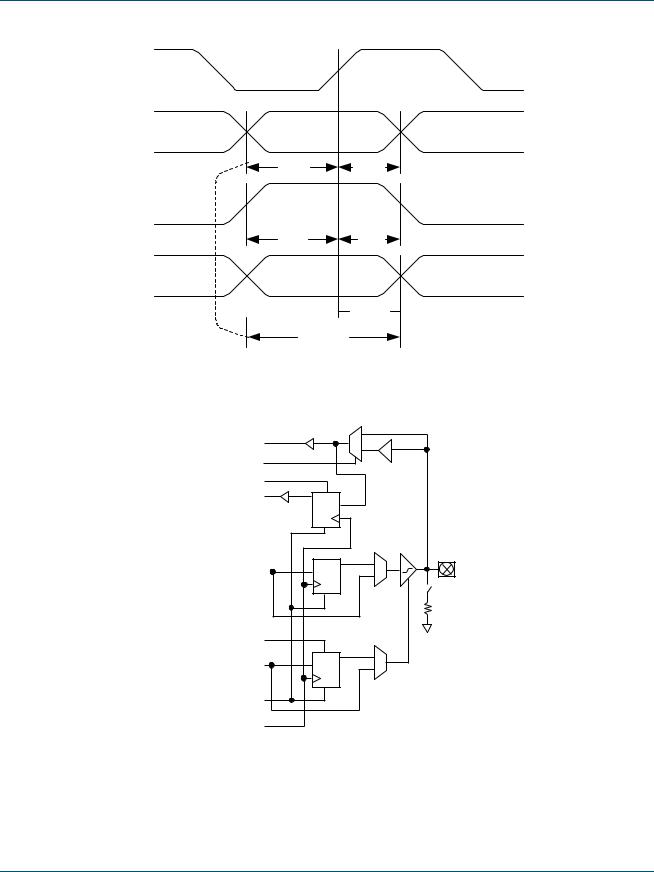
(PEHGGHG &RPSXWDWLRQDO 8QLW (&8
Traditional Programmable Logic architectures do not implement arithmetic functions efficiently or effectively—these functions require high logic cell usage while garnering only moderate performance results.
The QL7100 architecture allows for functionality above and beyond that achievable using programmable logic devices. By embedding a dynamically reconfigurable computational unit, the QL7100 device can address various arithmetic functions efficiently. This approach offers greater performance than traditional programmable logic implementations. The embedded block is implemented at the transistor level as shown in )LJXUH .
RESET |
|
|
D |
|
|
|
|
|
|
|
|
|
|
|
|
|
|
|
|
S1 |
|
3-4 |
C |
|
|
|
|
|
|
S2 |
|
B |
|
|
|
|
|
|
|
|
decoder |
|
|
|
|
|
|
||
S3 |
|
A |
|
|
|
|
|
|
|
|
|
|
|
|
|
|
|
||
CIN |
|
|
|
|
|
|
|
|
|
SIGN1 |
|
|
|
|
|
|
|
|
|
SIGN2 |
|
|
|
|
|
|
|
00 |
Q[0:16] |
|
|
|
|
|
|
|
|
|
|
|
|
|
|
|
|
|
|
01 |
3-1 |
|
|
|
|
|
|
|
|
|
mux |
|
A[0:7] |
8-bit |
2-1 |
16-bit |
|
D |
Q |
10 |
|
|
|
17 inc. |
17-bit |
|
|
||||
|
|
Multiplier |
mux |
Adder |
|
|
|||
|
A[8:15] |
COUT Register |
|
|
|||||
|
|
|
|
|
|
||||
A[0:15] |
|
|
|
|
|
|
|
|
|
CLK |
|
|
|
|
|
|
|
|
|
B[0:15] |
|
|
2-1 |
|
|
|
|
|
|
|
|
|
|
|
|
|
|
|
|
|
|
|
mux |
|
|
|
|
|
|
|
|
)LJXUH (&8 %ORFN 'LDJUDP |
|
|
|
|
|
||
The 10 QL7100 ECU blocks are placed next to the SRAM circuitry for efficient memory/instruction fetch and addressing for DSP algorithmic implementations.
Ten 8-bit Multiply-Accumulate (MAC) functions can be implemented per cycle for a total of 1 billion MACs/s when clocked at 100 MHz. Additional MAC functions can be implemented in the programmable logic.
The modes for the ECU block are dynamically re-programmable through the programmable logic as shown in 7DEOH .
W
‹ 4XLFN/RJLF &RUSRUDWLRQ ZZZ TXLFNORJLF FRP WW
W
W
W
 Loading...