


QUICK LOGIC QL5064-33APB456C, QL5064-33APB456I, QL5064-33APB484C, QL5064-33APB484I, QL5064-33BPB456C Datasheet
...4/ 4XLFN3&, 'DWD 6KHHW
W W W W W W 0+] ELW 3&, 0DVWHU 7DUJHW ZLWK (PEHGGHG 3URJUDPPDEOH /RJLF DQG GXDO 3RUW 65$0
'HYLFH +LJKOLJKWV
+LJK 3HUIRUPDQFH 3&, &RQWUROOHU ([WUHPHO\ )OH[LEOH DQG &RQILJXUDEOH
‡64-bit / 66 MHz Master/Target PCI Controller (automatically backwards compatible to 33 MHz or/and 32-bits)
‡75 MHz PCI Interface supported for embedded systems
‡PCI Specification v2.2 compliance
‡Programmable back-end interface with three 64-bit busses/100 MHz
‡Provides full 533 MB/s PCI data transfer rates (600 MB/s at 75 MHz)
$GYDQFHG 3&, )HDWXUHV
‡DMA Chaining mode for queued DMA transactions
‡Four-channel DMA mastering, plus a SPCI (Single PCI Access) mode
‡Unlimited bursts supported in Master and Target mode
‡Two Master Write FIFOs and two Master Read FIFOs, each 64-deep and 64 bits wide
‡Target Read and Write FIFOs for pre-fetched reads and multipleposted writes
‡Programmable interrupt controller
‡I2O compliant under microprocessor control
‡16 Mailbox registers for message passing and semaphores
‡Extended configuration space allowing Messaged Interrupts,
power management, and future PCI enhancement support
‡Supports processor-less systems, as well as 0 wait-state burst connections to all known 8/16/32/64 bit processors
‡Includes non-volatile on-chip configuration data for total customization
‡Independent PCI bus (66 MHz) and local bus (100 MHz) clocks
‡All local interface, control, and glue-logic can be implemented on chip
‡“PCI friendly” pinout simplifies board layout, supports 4-layer PCI boards
$GYDQFHG 0DVWHU '0$ )HDWXUHV
‡Programmable DMA Channel Arbitration Scheme
‡SPCI (Single PCI Access) mode may initiate any PCI Master command
‡DMA controller configurable via PCI or back-end
‡DMA Chaining mode allows a linked list of DMA transfers to occur without user intervention
+LJK 3HUIRUPDQFH 3&, 7DUJHW
‡Write posting FIFO increases performance with queued transactions
(up to 16 queued writes)
‡Any BAR can be defined as pre-fetchable
‡Six base address registers supported, configurable as memory or IO
‡Unique “Target Blast Mode” enables highperformance and very low overhead streaming data to/from PCI
W
W
4/ 4XLFN3&, 'DWD 6KHHW 5HY ' W
W
W
W
4/ 4XLFN3&, 'DWD 6KHHW
([SDQGHG 3&, )XQFWLRQDOLW\
‡Support for Configuration Space from 0x40 to 0x3FF
‡PCI expanded capabilities support
‡Expansion ROM supported with back-end memory
‡Power management support
‡Compact PCI hot-swap/hot-plug compliant
‡Messaged Interrupts
‡Configuration specified with anti-fuses on board, external EEPROM not needed
3URJUDPPDEOH /RJLF
‡192 Programmable I/O pins in a 456 pin or 484 pin PBGA package
‡74K gates with 11 blocks (total of 12,672 bits) of dual-port RAM
‡250 MHz 16-bit counters, 275 MHz Datapaths, 160 MHz FIFOS
‡All back-end interface and glue-logic can be implemented on chip
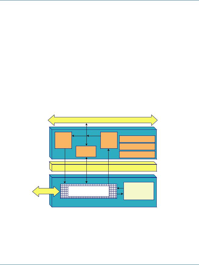
PCI Bus - 33/66/75 MHz 32/64 Bits (Data and Address) |
|||
3 RECV |
|
3 XMIT |
PCI CONTROLLER |
|
Interrupts |
||
FIFOs |
|
FIFOs |
|
|
|
||
64 deep |
|
64 deep |
Messaging |
|
4 Channel |
|
|
|
|
|
|
|
DMA Ctrl |
|
Config. |
64 |
64 |
64 |
100 MHz INTERFACE |
192 User I/O |
High Speed Logic Cells |
12k bits |
|
74K Gates |
Dual Port RAM |
||
|
|||
|
PROGRAMMABLE LOGIC |
|
Figure 1: QL5064 Block Diagram
W
W ZZZ TXLFNORJLF FRP ‹ 4XLFN/RJLF &RUSRUDWLRQ
W
W
W
W

4/ 4XLFN3&, 'DWD 6KHHW
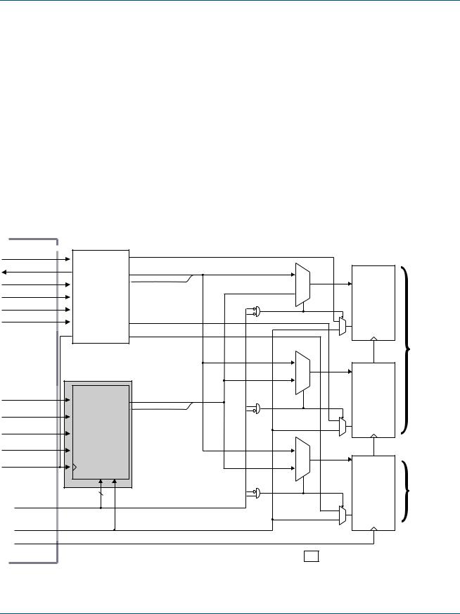
$UFKLWHFWXUH 2YHUYLHZ
The QL5064 device in the QuickLogic QuickPCI ESP (Embedded Standard Products) family provides a complete and customizable PCI interface solution combined with 74,000 system gates of programmable logic. This device eliminates any need for the designer to worry about PCI bus compliance, yet allows for the maximum possible PCI bus bandwidth.
The programmable logic portion of the device is built from 792 QuickLogic Logic Cells, and 11 QuickLogic Dual-Port RAM Blocks. The configurable RAM blocks can each operate in 64x18, 128x9, 256x4, or 512x2 mode. These dual-port RAM blocks can be cascaded to achieve deeper or wider configurations. They can also be combined with logic cells to form FIFOs. See the RAM section of this data sheet for more information.
The QL5064 device includes a complete pre-designed PCI Initiator/Target interface offering full burst mode transfers at 32 or 64 bits per clock cycle. At 66 MHz, this device offers support for 533 Mbytes/sec data transfer rates (66.6 MHz * 8 bytes per transfer). At the maximum speed of 75 MHz (exceeding the current maximum speed specification for PCI), the QL5064 device can achieve 600 Mbytes/sec data transfer rates. The PCI interface is configured via internal programmable configuration bits, so no external EEPROM or memory is needed.
The QL5064 device meets PCI 2.2 electrical and timing specifications and has been fully hardwaretested. This device also supports the Win’98 and PC’98 standards. The QL5064 device features 3.3- volt operation with multi-volt compatible I/Os. Thus it can easily operate in 3.3-volt only systems, as well as mixed 3.3 volt/5 volt system. It can be placed on a universal signaling PCI board.
A wide range of additional features complements the QL5064 device. The FPGA side of the device is 5 volt and 3.3-volt PCI-compliant and is capable of implementing FIFOs at 160 MHz, and counters at over 250 MHz. I/O pins provide individually controlled output enables, dedicated input/feedback registers, and full JTAG capability for boundary scan and test. In addition, the QL5064 device provides the benefits of non-volatility, high design security, immediate functionality on power-up, and a selfcontained single chip solution.
W
4/ 4XLFN3&, 'DWD 6KHHW 5HY ' W
W
W
W
W

4/ 4XLFN3&, 'DWD 6KHHW |
|
|
|
|
|
|
|
|
|
|
|
|
|
|
|
|
|
|
|
|
|||||||
|
|
|
|
|
|
|
|
|
|
|
|
|
User I/O (192) |
|
Global Clk's (4) |
|
|
Array Clk's (2) |
|
|
|
|
|
|
|
User clk (global clock) |
|
|
|
1152 bits |
|
1152 bits |
1152 bits |
|
1152 bits |
1152 bits |
|
1152 bits |
|
|
|
|
FPGA |
|
|
|
1152 bits |
1152 bits |
1152 bits |
1152 bits |
|
1152 bits |
|
Configuration |
|
|
|
|
Embedded Memory |
|
|
|
|
|
|
|
Embedded Memory |
|
|||||||||||||||
|
|
|
|
|
|
|
|
|
|
|
|
|
|
|
|
|
|
|
|
|
|
|
|
|
Antifuse |
||
|
|
|
|
|
|
|
|
|
|
|
|
|
|
(792 Logic Modules) |
|
|
|
|
|
|
|
|
|
||||
|
|
|
|
|
|
|
|
|
|
|
|
|
|
|
|
|
|
|
|
|
|
64 |
|
|
|
||
33 |
|
|
|
|
|
|
|
|
|
|
|
|
|
|
|
|
|
|
|
|
|
|
|
|
|
||
D Q |
|
|
|
data in Interface |
|
64 |
|
|
|
|
|
|
64 |
|
Registers 64 |
|
|
|
|
|
data out Interface |
Lane Steering |
|
|
|
|
|
|
|
|
|
|
|
Lane |
|
|
|
control Interface |
|
|
|
|
|
|
|
|
|
|
Clock(0-100MHz) |
PCI Clock |
|||||
|
|
|
|
|
|
Steering |
|
|
|
D Q |
|
|
Control Bus Decode |
|
|
Data Construction |
|
|
|||||||||
Address Latch/ |
Decode/ |
Increment |
|
|
|
|
|
|
|
|
|
|
|
|
|
|
|||||||||||
|
|
|
|
|
|
|
|
|
|
|
|
|
|
|
|
|
Prefetch |
|
|
|
|
|
|
|
|
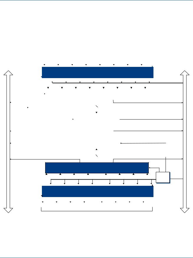
User |
|
|
|
72x32 |
Target |
Write/ |
Post FIFO |
72x64 |
DMA/ |
Chain Rcv0 |
FIFO |
72x64 |
DMA Rcv1 |
FIFO |
|
64x16 |
Target Read/ |
FIFO |
72x64 DMA/ |
Chain Xmit0 |
FIFO |
72x64 |
DMA Xmit1 |
FIFO |
|
|
|
||
Target Interface |
Controller |
|
|
Configuration |
|
|
5 DMA |
Controllers |
|
rcv1 |
Chain Control Single PCI Access |
|
|
|
|
|
|
PCI/FPGA Interrupt |
Controller |
|
PCI to FPGA |
Mailbox (8x8) |
FPGA to PCI |
Mailbox (8x8) |
Messaging |
||
|
|
|
|
|
xmit0 xmit1rcv0 |
|
|
Internal Bus Arbiter |
|
|
|
O |
|||||||||||||||
|
|
|
|
|
|
|
|
|
|
2 |
|||||||||||||||||
|
|
|
|
|
|
|
|
|
|
I |
|||||||||||||||||
|
|
|
|
|
|
|
|
|
|
|
PCI Interface Buffers & Logic |
|
|
|
|
|
|
|
|||||||||
33/66/75 MHz PCI 32/64 bits (data and address)
Figure 2: QL5064 Device Block Diagram
W
W ZZZ TXLFNORJLF FRP ‹ 4XLFN/RJLF &RUSRUDWLRQ
W
W
W
W

4/ 4XLFN3&, 'DWD 6KHHW
$SSOLFDWLRQV
The QL5064 device supports maximum PCI transfer rates, so many applications exist which are ideally suited to the device's high performance. High speed data communications, telecommunications, and computing systems are just a few of the broad range of applications areas that can benefit from the high speed PCI interface and programmable logic.
The PCI Interface can also act as a PCI Host Controller. This can be accomplished by glue-less interface to most popular 8/16/32/64-bit microprocessors.
6L[ ),)2V IRU ,QFUHDVHG 3HUIRUPDQFH
The PCI interface includes the following 6 FIFO buffers:
‡2 64x64 PCI Master Transmit Buffers
‡2 64x64 PCI Master Receive Buffers
‡1 16x64 PCI Target Read/Pre-Fetch Buffer
‡1 32x64 PCI Target Write/Post Buffer
All FIFO buffers are 72 bits wide (64 data bits + 8-bit byte enables). PCI Initiator-mode buffers are 64 deep and support sustained burst transfers. PCI Target mode buffers are provided for both Read and Write operations to the PCI Target, supporting pre-fetched reads with configurable registers.
All FIFOs can operate with independent read and write clocks, so that the programmable logic design can interface to the FIFOs at up to 100 MHz (a clock asynchronous to the 33/66 MHz PCI clock). All data synchronization is accomplished in the PCI core.
The transmit FIFOs have full flags and the receive FIFOs have empty flags. Both types of FIFOs have programmable status flags that may be used to determine if either of the transmit FIFOs are almost full or if either of the receive FIFOs are almost empty.
W
4/ 4XLFN3&, 'DWD 6KHHW 5HY ' W
W
W
W
W

4/ 4XLFN3&, 'DWD 6KHHW
'0$ )HDWXUH 2YHUYLHZ
Each Master-mode FIFO has its own DMA controller to support maximum data throughput. Combining one Initiator-Mode Transmit FIFO with one Initiator-Mode Receive FIFO also supports DMA Chaining. This unique and flexible DMA chaining mode permits a 'linked-list' of transfers to be completed by the DMA controller without software or processor intervention.
DMA Registers are accessible by the FPGA (back-end interface), as well as the PCI bus.
DMA Chaining descriptors are made of 4 64-bit Quad-Words, or 32 bytes of data per descriptor. Each descriptor defines a DMA transaction (memory start location, size, read/write) as well as 88 bits of userdefined information (such as a descriptor identifier, or back-end address).
DMA Chaining is a powerful DMA feature, allowing the QL5064 device to drive continuous pre-defined DMA transactions with no processor or software interaction.
Single PCI Access (SPCI) reads and writes are supported for single quad-word transfers that do not require FIFOs. SPCI supports IO reads and writes, configuration reads and writes, special cycles, interrupt acknowledge cycles, as well as standard memory read/write transactions.
63 |
|
|
|
|
0 Offset |
||
|
First PCI Address |
|
|
|
|
0 x 00 |
|
|
|
|
|
|
|
|
|
|
User Defined (63:0) |
|
|
|
|
0 x 08 |
|
|
(local address) |
7 |
|
|
0 |
|
|
|
Transfer Count (bytes) |
User Defined |
|
|
R |
E |
0 x 10 |
|
|
|
I |
O |
|||
|
(31:0) |
(23:0) |
|
|
|||
|
|
|
W |
C |
|
||
|
Next Descriptor Pointer Address (63:0) |
|
|
0 x 18 |
|||
Figure 3: DMA Chaining Descriptor
W
W ZZZ TXLFNORJLF FRP ‹ 4XLFN/RJLF &RUSRUDWLRQ
W
W
W
W
4/ 4XLFN3&, 'DWD 6KHHW
0DLOER[ 5HJLVWHUV DQG , 2
The PCI interface contains 16 bytes of mailbox registers to support message/semaphore passing between the programmable logic design and the PCI bus. These mailbox registers are memory mapped to a dedicated register bank within the first 256 bytes of BAR 0. 8 bytes are provided for the FPGA to PCI direction, and 8 bytes are also provided for the PCI to FPGA direction. Status flags and interrupts are available for each direction as well. Figure 4 below shows the mailbox structure within the QL5064 device. Hardware controlled queues allow full I2O messaging support with a processor and local I2O drivers.
|
|
|
|
|
|
|
|
|
|
|
|
|
|
|
|
|
|
|
|
|
|
|
|
|
|
|
|
|
|
|
|
|
|
|
|
|
|
|
|
|
|
|
|
|
|
|
|
|
|
|
|
|
|
|
|
|
|
|
|
|
|
|
|
|
|
|
|
|
|
|
|
|
|
|
|
|
|
|
|
|
|
|
|
|
|
|
|
|
|
63 |
|
|
|
|
|
|
|
|
|
|
|
|
|
|
|
|
|
|
|
|
|
|
|
|
|
0 |
|
|
|
|
||
|
|
|
|
|
|
|
|
byte 7 |
|
byte 6 |
byte 5 |
|
byte 4 |
|
byte 3 |
|
byte 2 |
byte 1 |
|
byte 0 |
|
|
|
|
||||||||||||||||
|
|
|
|
|
|
|
|
|
|
|
|
|
|
|
|
|
|
|
|
|
|
|
|
|
|
|
|
|
|
|
|
|
|
|
|
|
|
|
|
|
|
|
|
outgoing |
|
|
|
|
|
|
|
|
|
|
|
|
|
|
|
|
|
|
|
|
|
|
|
|
|
|
|
|
|
|
|
|
|
|
|||
|
|
|
|
|
|
|
|
|
|
|
|
|
|
|
|
|
|
|
|
|
|
|
|
|
|
|
|
|
|
|
|
|
|
|
|
|
||||
|
|
|
decode |
|
|
|
|
|
|
|
|
|
|
|
|
|
|
|
|
|
|
|
|
|
|
|
|
|
|
|
|
|
|
|
|
|||||
|
|
|
control |
|
|
|
|
|
|
|
|
|
|
|
|
|
|
|
|
|
|
|
|
|
|
|
|
|
|
|
|
|
|
|
|
|
|
|||
|
|
|
|
|
|
|
|
|
|
|
|
|
|
|
|
|
|
|
|
|
|
|
|
|
|
|
|
|
|
|
|
|
|
|
|
|
|
|
|
|
|
|
|
|
|
|
|
|
|
|
|
|
|
|
|
|
|
|
|
STATUS REGISTER |
|
|
|
|
|
|
|
|
|
|
|
|
|
|
|
||||||
|
|
|
|
|
|
|
|
|
|
|
|
|
|
|
|
|
|
|
|
|
|
|
|
|
|
|
|
|
|
|
|
|
|
|||||||
|
|
|
|
|
|
|
|
|
|
|
|
|
|
|
|
|
|
|
|
|
|
|
|
|
|
|
|
|
|
|
|
|
|
|
|
|
|
|
|
|
|
|
|
|
|
|
|
|
|
|
|
|
|
|
|
|
|
|
|
|
|
|
|
|
|
|
|
|
|
|
|
|
status |
|
|
|
|
|
|
|
|
|
|
|
|
|
|
|
|
|
|
|
|
|
status |
|
|
|
|
|
|
|
8 |
|
|
|
|
|
|
|
|
|
|
|
|
|
|
|
|
|||
|
|
interrupt |
|
|
|
|
|
|
|
|
|
|
|
|
|
|
|
|
|
|
|
|
|
|
|
|
|
|
|
|
|
|
|
|
|
|
|
|||
|
|
|
|
|
|
|
|
|
|
|
|
|
|
|
|
|
|
|
|
|
|
|
|
|
|
|
|
|
|
|
|
|
|
|||||||
|
|
configuration |
|
|
|
|
|
|
|
|
|
|
|
|
|
|
|
|
|
|
|
|
|
|
|
|
|
|
|
|
|
full interrupt |
||||||||
|
|
|
register |
|
|
|
|
|
|
|
|
|
INTERRUPT CONTROL |
|
|
|
|
|
|
|
|
|
|
|
|
|||||||||||||||
|
|
|
|
|
|
empty interrupt |
|
|
|
|
|
|
|
|
|
|
|
|
|
empty interrupt |
||||||||||||||||||||
|
|
|
|
|
|
|
|
|
|
|
|
|
|
|
|
|
|
|
|
|
|
|
|
|
|
|
||||||||||||||
|
|
|
|
|
|
|
|
|
|
|
|
|
|
|
|
|
|
|
|
|
|
|
|
|
|
|
||||||||||||||
|
|
|
|
|
|
|
|
|
|
|
|
|
|
|
|
|
|
|
|
|
|
|
|
|
|
|
||||||||||||||
|
|
full interrupt |
|
|
|
|
|
|
|
|
|
|
|
|
|
|
|
|
|
|
|
|
|
|
|
|
|
|
|
|
|
|||||||||
|
|
|
|
|
|
|
|
|
|
|
|
|
|
|
|
|
|
|
|
|
|
|
|
|
|
|
|
|
interrupt |
|
||||||||||
|
|
|
|
|
|
|
|
INTERRUPT CONTROL |
|
|
|
|
|
|
|
|
|
|
|
|
|
|
||||||||||||||||||
|
|
|
|
|
|
|
|
|
|
|
|
|
|
|
|
|
|
|
|
|
|
|
|
|
|
|
|
|
|
|
configuration |
|
||||||||
|
|
|
|
|
|
|
|
|
|
|
|
|
|
|
|
|
|
|
|
|
|
|
|
|
|
|
|
|
|
|
|
|
|
|
|
|
|
|
|
|
|
|
|
|
|
|
|
|
|
|
|
|
|
|
|
|
|
|
|
|
|
|
|
|
|
|
|
|
|
|
|
|
|
|
|
|
|
|
|
register |
|
|
|
|
|
|
|
|
|
|
|
|
|
|
status |
|
|
|
|
|
|
8 |
|
|
|
|
|
|
|
|
|
|
status |
|
|
|
|
|
|
|
|
|
|
|
|
|
|
|
|
|
|
|
|
|
|
|
|
|
|
|
|
|
|
|
|
|
|
|
|
|
|
|
|
|
|
|
|
|
|
||||
|
|
|
|
|
|
|
|
|
|
|
|
|
|
|
|
|
|
|
|
|
|
|
|
|
|
|
|
|
|
|
|
|
|
|
|
|
||||
|
|
|
|
|
|
|
|
|
|
|
|
|
|
|
|
|
|
|
|
|
|
|
|
|
|
|
|
|
|
|
|
|
|
|
|
|
|
|||
|
|
|
|
|
|
|
|
|
|
|
|
|
|
|
|
|
|
|
|
|
|
|
|
|
|
|
|
|
|
|
|
|
|
|
|
|
|
|
|
|
STATUS REGISTER
incoming decode control
|
63 |
|
|
|
|
|
|
|
|
|
|
|
|
0 |
|
||
|
|
byte 7 |
|
byte 6 |
|
byte 5 |
|
byte 4 |
byte 3 |
byte 2 |
byte 1 |
byte 0 |
|
||||
|
|
|
|
|
|
|
|
|
|
|
|
|
|
|
|
|
|
|
|
|
|
|
|
|
|
|
|
|
|
|
|
|
|
|
|
|
|
|
|
|
|
|
|
|
|
|
|
|
|
|
|
|
|
|
|
|
|
|
|
|
|
|
|
|
|
|
|
|
|
|
|
mailbox 7 |
mailbox 6 mailbox 5 mailbox 4 mailbox 3 mailbox 2 mailbox 1 mailbox 0 |
PCI BUS |
User Outgoing mailboxes |
Figure 4: Mailbox Structure
CNTL BUS
W
4/ 4XLFN3&, 'DWD 6KHHW 5HY ' W
W
W
W
W
4/ 4XLFN3&, 'DWD 6KHHW
4/ ,QWHUQDO %XV 6WUXFWXUH
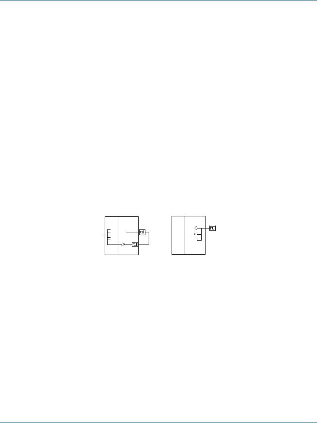
The internal interface between the PCI Controller and the FPGA logic cells is both simple and flexible. The interface is configurable, based on the needs of the FPGA design. Configuration is accomplished at the time of programming the FPGA.
The FPGA/PCI interface supports very high bandwidth data transfers via 3 64-bit busses. The interface is totally synchronous, and supports a separate clock from the PCI clock. The Interface clock can run at up to 100 MHz.
These busses are called DataIN, DataOUT, and Control_DATA. The DataIN bus is for moving data from the PCI bus to the back-end. The DataOUT bus is for moving data from the back-end to the PCI bus. The Control_DATA bus is for both of the above, and for accessing internal control registers. All 3 busses can operate at 0 wait states, and all can operate at the same time.
4/ &ORFNLQJ
All bus accesses to the QL5064 from the FPGA (back-end) interface are synchronous to the back-end user clock - called user_clk. This clock is supplied on a dedicated external pin. The PCI clock may be routed out to a pin, and then back into the device to be used as the user_clk if desired. The user_clk signal may be asynchronous to the pci_clk signal, and may run at up to 100 MHz with no PLL requirements.
All busses on the back-end of the QL5064 device can sustain data movement on every cycle of user_clk.
PCI |
FPGA |
|
user_clk |
pci_clk |
or |
user_clk
PCI FPGA user_clk
osc
Figure 5: FPGA to PCI Synchronization
W
W ZZZ TXLFNORJLF FRP ‹ 4XLFN/RJLF &RUSRUDWLRQ
W
W
W
W
4/ 4XLFN3&, 'DWD 6KHHW
'DWD,1 %XV 'HVFULSWLRQ
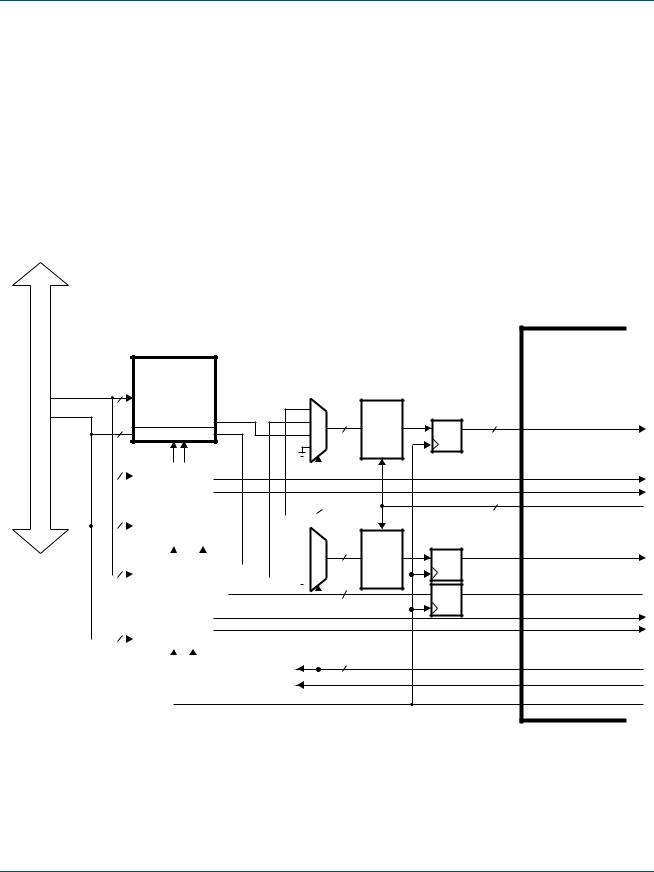
The DataIN bus is used to transfer data from the PCI bus to the back-end interface. This data can come from three different data paths: one of the two DMA receive FIFOs, or the Target Write/Post FIFO. For proper data management, empty and almost empty flags from the two DMA receive FIFOs are available to the back-end design. The almost empty flags are fully configurable via the Control_DATA bus interface or the PCI bus. Interface to the Target Write/Post FIFO is accomplished through the Target interface signals. A block diagram of the DataIN and Target control connections is seen in Figure 6.
Data is transferred to the DataIN bus in the same byte lane in which is was transferred over the PCI bus. To assist with re-aligning or compacting data in the back-end interface, a byte-lane barrel shifter provides the means to manipulate byte lane positioning. This is accomplished with the byte_select[2:0] input.
See the DataIN Bus section of the internal signal descriptions for more information.
Bus PCI
|
|
Target/ |
|
pci data |
64 |
Write |
|
pci cbe [7:0] |
|
Post FIFO |
0 |
|
(32 Deep) |
||
|
|
||
|
8 |
1 |
|
|
Byte lane [7:0] |
2 |
|
|
|
||
|
|
|
3 |
64 |
|
|
|
|
|
|
|
|
|
|
|
|
|
|
|
|
|
|
|
|
|
|
DMA Rcv 0 |
|
|
|
|
|
|
|
|
|
|
|
|
|
|
|
|
||||||
|
|
|
|
|
|
|
|
|
|
|
|
|
|
|
|
|
|
|||||
|
|
|
|
|
|
|
|
|
|
|
|
|
|
|
|
|
|
|||||
|
|
FIFO |
|
|
|
|
|
|
|
|
|
|
|
|
|
|
|
|
||||
|
|
(64 deep) |
|
|
|
|
|
|
|
|
|
|
|
|
|
|
|
2 |
||||
8 |
|
|
|
|
|
|
|
|
|
|
||||||||||||
|
|
|
|
|
|
|
|
|
|
|
|
|
|
|
|
|
|
|
|
|
||
|
|
Byte lane [7:0] |
|
|
|
|
|
|
|
|
|
|
|
|
|
|
0 |
|
||||
|
|
Chain Descriptor Tags |
|
|
|
|
|
|
|
|
|
|
||||||||||
|
|
|
|
|
|
|
|
|
|
|
|
|
|
|
|
1 |
|
|||||
64 |
|
|
|
|
|
|
|
|
|
|
|
|
|
|
2 |
|
||||||
|
|
|
|
|
|
|
|
|
|
|
|
|
|
|
|
|
|
3 |
|
|||
|
|
DMA Rcv 1 |
|
|
|
|
|
|
|
|
|
|
|
|||||||||
|
|
|
|
|
|
|
|
|
|
|
|
|
|
|
|
|
|
|||||
|
|
or Target Write |
|
|
|
|
|
|
|
|
|
|
|
|
|
|
|
|
||||
|
|
|
|
|
|
|
|
|
|
|
|
|
|
|
|
|
|
|||||
|
|
Post FIFO |
|
|
|
|
|
|
|
|
|
|
|
|
|
|
|
|
||||
|
|
(64 Deep) |
|
|
|
|
|
|
|
|
|
|
|
|
|
|
|
|
||||
8 |
|
|
|
|
|
|
|
|
|
|
|
|
|
|
|
|
|
|
|
|
|
|
|
|
Byte lane [7:0] |
|
|
|
|
|
|
|
|
|
|
|
|
|
|
|
|
||||
|
|
|
|
|
|
|
|
|
|
|
|
|
|
|
|
|
|
|||||
|
|
|
|
|
|
|
|
|
|
|
|
|
|
|
|
|
|
|||||
|
|
|
|
|
|
|
|
|
|
|
|
|
|
|
|
|
|
|
|
|
|
|
|
|
|
|
|
|
|
|
|||||||||||||||
|
|
|
|
|
|
|
|
|
|
2 |
Decode |
|
|
|
|
|
|
|
|
|
||
|
|
|
|
|
|
|
|
|
|
0 |
|
|
|
|
|
|
|
|
|
|
|
|
|
|
|
|
|
|
|
|
|
|
1 |
|
|
|
|
|
|
|
|
|
|
|
|
|
|
|
|
|
|
|
|
|
|
|
|
|
|
|
|
|
|
|
|
|
|
|
|
|
|
|
|
|
|
|
|
|
|
|
|
|
|
|
|
|
|
|
|
|
|
|
|
|
|
FPGA |
|
64 |
Lane |
|
64 |
dataIN [63:0] |
|
Barrel |
D |
||||
|
Q |
|
|||
|
Shifter |
|
|
|
|
|
|
|
|
rcv0_fifo_program_empty_flag |
|
|
|
|
|
rcv0_fifo_ef |
|
|
|
|
3 |
dataIN_bytesel [2:0] |
|
8 |
Shifter |
D |
Q |
dataIN_BE[7:0] |
|
|
|
||||
2 |
|
D |
Q |
dataIN_byteID [1:0] |
|
|
|
|
|||
|
|
|
|
rcv1_fifo_program_empty_flag |
|
|
|
|
|
rcv1_fifo_ef |
2 |
dataIN_src_sel[1:0] |
|
dataIN_cs |
|
user_clk |
Figure 6: DataIN Bus Description
W
4/ 4XLFN3&, 'DWD 6KHHW 5HY ' W
W
W
W
W
4/ 4XLFN3&, 'DWD 6KHHW
'DWD287 %XV 'HVFULSWLRQ
The DataOUT bus is used to transfer data from the back-end interface to the PCI bus. This bus is connected to three destinations within the QL5064 device: one of the two DMA transmit FIFOs, or the Target Read/Pre-Fetch FIFO. For proper data management and high data throughput, full and almost full flags are available for each of the two DMA transmit FIFOs. The almost full flags are fully configurable via the Control_DATA bus interface or the PCI bus. Interface to the Target Read/Pre-Fetch FIFO is accomplished through the Target interface signals. A block diagram of the DataOUT connections can be seen in Figure 7.
The data_outDES[1:0] signals select a particular FIFO to be connected to the DataOUT bus. A block diagram of the DataOUT bus and its connections can be seen in Figure 7.
Data written to the DMA transmit FIFOs or the Target Read/Pre-fetch FIFO must be set up in the same byte lanes in which the data will be transferred in the PCI bus. To aid with aligning, re-aligning, or compacting data that is to be written to the FIFOs via the DataOUT bus, a byte-lane barrel shifter is present, controlled by the data_out_shift[2:0] signals. See the DataOUT bus section of the internal signal descriptions table for more information.
cntl_data_in [63:0] |
|
(cntl_addr == 0xc0 ) * ctrl_cs |
|
cntl_data_out [63:0] |
|
cntl_data[63:0] |
0 |
|
|
||
|
|
byte_lane [7:0] |
|
cntl_wrt_nrd |
|
|
|
Control |
|
|
|
cntl_be[7:0] |
|
1 |
|
Bus |
|
||
|
|
|
|
cntl_addr [7:3] |
Interface |
|
0 |
|
|
||
|
|
|
1 |
cntl_cs |
|
(cntl_addr == 0xc8 ) * ctrl_cs |
0 |
|
|
(cntl_addr == 0xf8) * ctrl_cs |
1 |
|
|
|
|
|
|
|
0 |
|
|
|
1 |
data_out [63:0] |
|
data_out_h [63:0] |
|
|
|
|
|
|
data_out |
data_out_BEh[7:0] |
0 |
|
1 |
||
|
|
||
data_out_BE[7:0] |
Lane |
|
|
|
|
0 |
|
data_out_byte_sel[2:0] |
Shifter |
|
1 |
fpga_reset |
& |
|
|
Construction |
|
0 |
|
|
|
||
user_clk |
|
|
1 |
|
|
|
|
|
2 |
|
0 |
|
|
1 |
|
data_outDES[1:0] |
|
|
|
|
|
|
0 |
|
|
|
1 |
data_outCS |
|
|
|
user_clk |
|
|
|
Fifo 0
Transmit
WR
To Master
Controller
Fifo 1
Transmit
WR
Target |
To Target |
|
Read |
||
Controller |
||
Fifo |
||
|
WR
FPGA |
PCI Core |
|
|
||
|
|
|
Detailed in Figure 3–17
Figure 7: DataOUT and Control Bus Description
W
W ZZZ TXLFNORJLF FRP ‹ 4XLFN/RJLF &RUSRUDWLRQ
W
W
W
W
4/ 4XLFN3&, 'DWD 6KHHW
&RQWUROB'DWD %XV 'HVFULSLWRQ
The Control_DATA bus is the heart of the control circuitry for the PCI interface. The intent of this bus is to provide access to all of the control structures necessary for a microprocessor interfaced to the QL5064 device to be able to marshal all PCI operations. This bus, like the DataIN and DataOUT busses is synchronous to user_clk, and can be written or read on every clock. This is a bi-directional bus, offering both read and write access at 64-bits. In addition to all control structures, this bus is designed to access all of the six FIFOs.
3&, 0DVWHU $UELWUDWLRQ
Five possible masters could be driving PCI master transactions on the PCI bus, and as a result, a flexible arbitration controller has been included in the QL5064 device. The five sources for PCI master transactions include: Transmit FIFO 0, Transmit FIFO 1, Receive FIFO 0, Receive FIFO 1, and SPCI (Single PCI Access). (SPCI is a means for the back end-design to initiate single quad-word transfers directly on the PCI bus for master transactions, bypassing the DMA FIFOs). SPCI Mastering is controlled through the Control_DATA bus.
Three arbitration modes have been defined for the QL5064 device. These are round robin, prioritized, and customized. In all modes, the SPCI Mastering always has highest priority. The arbitration scheme is selected by setting the proper values in the Arbitration Mode bits of configuration registers (offset 0xD0, bits 49:48). The selection is: 00b - round robin, 01b - prioritized, 10b - customized, 11b - reserved.
Round robin arbitration simply cycles through the four Master FIFOs in the following order: Transmit 0 (T0), Transmit 1 (T1), Receive 0 (R0), Receive 1 (R1). Prioritized mode uses values assigned to DMA_arbitration_priority bits in the configuration memory (offset 0xD0). Masters set to equal priority are arbitrated (high to low): T0, T1, R0, R1.
Customized arbitration mode uses two busses and back-end logic. The fpga_bus_req[3:0] signals (1 bit per FIFO) indicate to the programmable logic design which master is requesting the bus. The fpga_bus_req bits are assigned: [0]-R1, [1]-R0, [2]-T1, [3]-T0. The back-end design should set fpga_arb_sel[1:0] according to which master should be granted the bus. The fpga_arb_sel bus uses the enumeration: 00-R1, 01-R0, 10-T1, 11-T0.
W
4/ 4XLFN3&, 'DWD 6KHHW 5HY ' W
W
W
W
W
4/ 4XLFN3&, 'DWD 6KHHW
&RQWURO 5HJLVWHUV
DMA Control and QL5064 registers can be accessed from the PCI bus or the back-end Control_DATA bus. On the PCI side, these registers are accessed off of BAR 0, with offets 0x00 to 0xFF (below 0x100). The breakdown of this memory space can be seen in the following table.
USER Memory Map
63 |
62 |
61 |
60 |
59 |
58 |
57 |
56 |
55 |
54 |
53 |
52 |
51 |
50 |
49 |
48 |
47 |
46 |
45 |
44 |
43 |
42 |
41 |
40 |
39 |
38 |
37 |
36 |
35 |
34 |
|
33 |
32 |
31 |
30 |
29 |
28 |
27 |
26 |
25 |
24 |
23 |
22 |
21 |
20 |
19 |
18 |
17 |
16 |
15 |
14 |
13 |
12 |
11 |
10 |
9 |
8 |
7 |
6 |
5 |
4 |
3 |
2 |
1 |
0 |
|
||||||||
|
|
|
|
|
|
|
|
|
|
|
|
|
|
|
|
|
|
|
|
|
|
|
|
|
|
|
|
|
|
|
|
|
|
|
|
|
|
|
|
|
|
|
|
|
|
|
|
|
|
|
|
|
|
|
|
|
|
|
|
|
|
|
|||||||||||
|
|
|
|
|
|
|
|
|
|
|
|
|
|
|
|
|
|
|
|
|
Master Write Address 0[63:0] (r/w) |
|
|
|
|
|
|
|
|
|
|
|
|
|
|
|
|
|
|
|
|
|
00 |
||||||||||||||||||||||||||||||
|
|
|
|
|
Master Write Count Status0[31:0] (r only) |
|
|
|
|
|
|
|
|
|
Master Write Transfer Count0[31:0] (r/w) |
|
|
|
|
|
08 |
||||||||||||||||||||||||||||||||||||||||||||||||||||
|
|
|
|
|
|
|
|
|
|
|
|
|
|
|
|
|
|
|
|
|
|
|
|
|
|
|
|
|
|
|
|
|
|
|
|
|
|
|
|
|
|
|
|
|
|
|
|
|
|
|
|
|
|
|
|
|
|
|
|
|
|
|
|||||||||||
|
|
|
|
|
|
|
|
|
|
|
|
|
|
|
|
|
|
|
|
|
Master Write Address 1[63:0] (r/w) |
|
|
|
|
|
|
|
|
|
|
|
|
|
|
|
|
|
|
|
|
|
10 |
||||||||||||||||||||||||||||||
|
|
|
|
|
Master Write Count Status1[31:0] (r only) |
|
|
|
|
|
|
|
|
|
Master Write Transfer Count1[31:0] (r/w) |
|
|
|
|
|
18 |
||||||||||||||||||||||||||||||||||||||||||||||||||||
|
|
|
|
|
|
|
|
|
|
|
|
|
|
|
|
|
|
|
|
|
|
|
|
|
|
|
|
|
|
|
|
|
|
|
|
|
|
|
|
|
|
|
|
|
|
|
|
|
|
|
|
|
|
|
|
||||||||||||||||||
|
|
|
|
|
|
|
Single PCI Access |
|
|
|
|
Receive FIFO 1 |
|
Bus Request |
Not Empty |
tag0 |
|
Receive FIFO 0 |
|
|
|
|
|
|
|
|
|
Chip Revision ID [7:0] |
User ID [7:0] (r only) |
|
|||||||||||||||||||||||||||||||||||||||||||
00 |
|
|
|
|
|
|
|
|
|
|
|
|
|
|
|
|
|
|
|
|
|
|
|
|
|
|
|
|
|
|
|
|
Pipeline |
|
|
|
|
|
|
|
|
|
|
|
|
|
|
|
|
|
|
|
|
|
|
|
|
|
|
|
|
|
|
|
|
|
|
|
|
|
20 |
||
|
|
|
|
|
|
|
|
|
|
|
|
|
|
|
|
Byte Lane[7:0] |
|
|
|
|
|
|
[1:0] |
|
Byte Lane[7:0] |
|
XM f |
XM a f |
XM f |
XM a f |
RC e |
RC a e |
RC e |
RC a e |
|
|
|
(r only) |
|
|
|
|
|
antifuse |
|
|
|||||||||||||||||||||||||||
strt |
32 |
cmd[3:0] |
|
byte lanes[7:0] |
|
|
|
XMT |
XMT |
RCV |
RCV |
XMT |
XMT |
|
|
|
|
|
|
|
|
|
|
|
|
||||||||||||||||||||||||||||||||||||||||||||||||
|
|
|
|
bit |
|
|
|
|
0 |
|
1 |
|
0 |
|
1 |
0 |
1 |
|
|
|
|
|
|
|
|
|
|
|
|
|
|
|
|
|
|
|
|
|
|
||||||||||||||||||||||||||||||||||
0000 |
en16 /8 |
wrt |
wwt |
BAR Enable (r only) |
|
|
|
Target BAR Configuration (r only) |
|
|
|
|
Target FIFO |
Target FIFO Control -- Emptyness Threshold |
0 |
Target Prefetch Cntl |
0 |
Target Burst Request |
28 |
||||||||||||||||||||||||||||||||||||||||||||||||||||||
|
|
|
|
|
|
|
|
Threshold |
|||||||||||||||||||||||||||||||||||||||||||||||||||||||||||||||||
rom |
5 |
4 |
3 |
2 |
1 |
0 |
|
BAR5 |
BAR4 |
|
BAR3 |
BAR2 |
|
BAR1 |
|
BAR0 |
|
MSB's[3:0] |
BAR5 |
BAR4 |
BAR3 |
BAR2 |
BAR1 |
BAR0 |
|
RO |
|
|
BAR[5:0] |
|
|
|
RO |
|
|
BAR[5:0] |
|
||||||||||||||||||||||||||||||||||||
|
|
|
|
|
|
|
|
|
|
I2O Interrupt Mask Bit [3] |
|
|
|
|
|
|
|
|
|
|
|
|
|
|
|
|
|
|
I2O Interrupt Service Request Bit [3] |
|
|
|
|
|
|
|
30 |
||||||||||||||||||||||||||||||||||||
|
|
|
|
|
|
|
|
|
|
|
|
|
|
|
|
|
|
|
|
|
|
|
|
|
|
|
|
|
|
|
|
|
|
|
|||||||||||||||||||||||||||||||||||||||
|
|
|
|
|
|
|
|
|
|
|
|
|
|
|
|
|
|
|
|
|
|
|
|
|
|
|
|
|
|
|
|
|
|
Reserved |
|
|
|
|
|
|
|
|
|
|
|
|
|
|
|
|
|
|
|
|
|
|
|
|
|
|
|
|
|
|
38 |
||||||||
|
|
|
|
|
|
|
|
|
I2O Outbound Queue Pointer |
|
|
|
|
|
|
|
|
|
|
|
|
|
|
|
|
|
|
|
|
I2O Inbound Queue Pointer |
|
|
|
|
|
|
|
|
|
|
40 |
||||||||||||||||||||||||||||||||
|
|
|
Master Read Address 0[63:0] (r/w) / Chain Descriptor Start Address [63:0] (r/w) |
|
|
48 |
|||||||||||||||||||||||||||||||||||||||||||||||||||||||||||||||||||
|
|
|
|
|
Master Read Count Status0[31:0] (r only) |
|
|
|
|
|
|
|
|
Master Read Transfer Count0[31:0] (r/w) |
|
|
|
|
|
50 |
|||||||||||||||||||||||||||||||||||||||||||||||||||||
|
|
|
|
|
|
|
|
|
|
|
|
|
|
|
|
|
|
|
|
|
|
|
|
|
|
|
|
|
|
|
|
|
|
|
|
|
|
|
|
|
|
|
|
|
|
|
|
|
|
|
|
|
|
|
|
|
|
|
|
|
|
|
|||||||||||
|
|
|
|
|
|
|
|
|
|
|
|
|
|
|
|
|
|
|
|
|
Master Read Address 1[63:0] (r/w) |
|
|
|
|
|
|
|
|
|
|
|
|
|
|
|
|
|
|
|
|
|
58 |
||||||||||||||||||||||||||||||
|
|
|
|
|
Master Read Count Status1[31:0] (r only) |
|
|
|
|
|
|
|
|
Master Read Transfer Count1[31:0] (r/w) |
|
|
|
|
|
60 |
|||||||||||||||||||||||||||||||||||||||||||||||||||||
|
|
|
|
|
|
|
|
|
|
|
|
|
|
|
|
|
|
|
|
|
|
|
|
|
|
|
|
|
|
|
|
|
|
|
|
|
|
|
|
|
|
|
|
|
|
|
|
|
|
|
|
|
|
|
|
|
|
|
|
|
|
|
|
||||||||||
00 |
|
|
XMIT FIFO 1 |
|
00 |
|
XMIT FIFO 0 |
|
00 |
|
XMIT FIFO 1 |
|
00 |
|
|
|
XMIT FIFO 0 |
|
00 |
|
Receive FIFO1 |
|
00 |
|
Receive FIFO0 |
|
00 |
|
Receive FIFO1 |
|
00 |
|
Receive FIFO0 |
|
68 |
||||||||||||||||||||||||||||||||||||||
|
|
Almost Full[5:0] |
|
|
Almost Full[5:0] |
|
Almost Empty[5:0] |
|
|
Almost Empty[5:0] |
|
Almost Full[5:0] |
|
|
Almost Full[5:0] |
|
|
Almost Empty[5:0] |
|
|
Almost Empty[5:0] |
||||||||||||||||||||||||||||||||||||||||||||||||||||
|
|
|
|
|
(r/w) |
|
|
|
|
|
|
|
(r/w) |
|
|
|
|
|
|
|
(r/w) |
|
|
|
|
|
|
|
|
|
|
(r/w) |
|
|
|
|
|
|
|
(r/w) |
|
|
|
|
|
|
(r/w) |
|
|
|
|
|
|
|
(r/w) |
|
|
|
|
|
|
|
|
(r/w) |
|
|
|
||||||
User Incoming Mail 7 |
User Incoming Mail 6 |
User Incoming Mail 5 |
User Incoming Mail 4 |
User Incoming Mail 3 |
User Incoming Mail 2 |
User Incoming Mail 1 |
User Incoming Mail 0 |
70 |
|||||||||||||||||||||||||||||||||||||||||||||||||||||||||||||||||
|
|
|
|
|
|
|
|
|
|
|
|
|
|
|
|
|
|
|
|
|
|
|
|
|
|
|
|
|
|
|
|
|
|
|
|
|
|
|
|
|
|
|
|
|
|
|
|
|
|
||||||||||||||||||||||||
User Outgoing Mail 7 |
User Outgoing Mail 6 |
User Outgoing Mail 5 |
User Outgoing Mail 4 |
User Outgoing Mail 3 |
User Outgoing Mail 2 |
User Outgoing Mail 1 |
User Outgoing Mail 0 |
78 |
|||||||||||||||||||||||||||||||||||||||||||||||||||||||||||||||||
|
|
|
|
|
|
|
|
|
|
|
|
|
|
|
|
|
|
|
|
|
|
|
|
|
|
|
|
|
|
|
|
|
|
|
|
|
|
|
|
|
|
|
|
|
|
|
|
|
|
|
|
|
|
|
|
|
|
|
|
|
|
|
|
|
|
|
|
|
|
|
|
|
|
0000_0000
0000_0000
0000 |
PED |
MRT |
MA |
RTA |
|
|
|
|
|
0000_0000
0000_0000 |
0000_0000 |
0000_0000 |
0000 |
I2O Interrupt |
|
SP I |
|
DMA Interrupt |
User Outgoing MB |
||||||||||||||||||
oflf |
ople |
iplf |
ifle |
BI St |
CE |
chn |
rcv1 |
rcv0 |
xmt1 |
xmt0 |
Empty [7:0] |
||||||||||||||||
0000_0000 |
PCI Incoming MB Empty |
PCI Outgoing MB Empty |
0000 |
I2O Int Mask |
BI Ms |
|
DMA Interrupt Mask User Outgoing MB Empty |
||||||||||||||||||||
|
Interrupt Mask[7:0] |
Interrupt Mask[7:0] |
oflf |
ople |
iplf |
ifle |
SP Ma |
CE |
chn |
rcv1 |
rcv0 |
xmt1 |
xmt0 |
Interrupt Mask[7:0] |
|||||||||||||
|
|
|
Error |
|
|
|
|
|
User region |
|
|
|
|
|
|
|
|
Ptr |
|
|
|
|
|
User Outgoing MB |
|||
|
|
|
|
|
|
|
|
|
|
I2O Status |
|
|
DMA Start/Done# |
||||||||||||||
|
|
|
|
|
|
|
|
|
|
|
|
|
user_be_req[7:0] |
|
|
|
|
|
|
|
Chain |
|
|
|
|
|
|
|
|
|
|
|
|
|
|
|
|
|
|
[2:0] |
|
|
|
|
|
|
|
Fetch |
|
|
|
|
|
|
|
00 |
SPCI |
Chn |
rcv1 |
rcv0 |
xmt1 |
xmt0 0 |
TUR W |
TAV |
TUR |
TUM |
|
|
0000 |
oflf |
ople |
iplf |
ifle |
BI St 0 End |
chn |
rcv1 |
rcv0 |
xmt1 |
xmt0 |
Status [7:0] |
|||
Single PCI Access Address Register[63:0] (r/w)
Single PCI Access Data Register[63:0] (r/w)
Reserved
Receive FIFO0[63:0] (r only)
Receive FIFO1[63:0] (r only)
Transmit FIFO0[63:0] (w only)
Transmit FIFO1[63:0] (w only)
|
Arb |
DMA Arbitration Priority |
|
DMA 32/64# |
|
|
DMA |
SPC |
|
FIFO |
|
DMA Cancel |
|
|
BIST |
|||||||||
|
|
|
|
|
Flush |
|
|
|
||||||||||||||||
0000_00 |
Mode |
rcv1[1:0] |
rcv0[1:0] |
xmt1[1:0] |
xmt0[1:0] |
0000 |
rcv1 |
rcv0 |
xmt1 |
xmt0 |
0000 |
rcv1 |
rcv0 |
xmt1xmt0 |
0 |
xmt1xmt0 |
Chn |
rcv1 |
rcv0 |
xmt1 |
xmt0 |
000 |
BI Do |
Code[3:0] |
[1:0] |
||||||||||||||||||||||||
Reserved
Reserved
Reserved
Target Control Address[63:0] (r only)
Target Control Data[63:0] (r/w)
|
User Incoming MB |
|
80 |
||||
|
|
Full [7:0] |
|
|
|
||
User Incoming MB Full |
|
88 |
|||||
Interrupt Mask[7:0] |
|
||||||
|
User Incoming MB |
|
90 |
||||
|
Status [7:0] |
|
|||||
|
|
|
|
|
|
|
98 |
|
|
|
|
|
|
|
a0 |
|
|
|
|
|
|
|
a8 |
|
|
|
|
|
|
|
b0 |
|
|
|
|
|
|
|
b8 |
|
|
|
|
|
|
|
c0 |
|
|
|
|
|
|
|
c8 |
|
|
|
|
|
|
|
|
|
BE En |
Max |
FIFO |
|
lat |
|
|
|
Retry |
Thresh |
|
|
|||
0 |
[1:0] |
|
|
en d0 |
|||
|
[1:0] |
TO[1:0] |
|
||||
|
|
|
|
|
|
|
d8 |
|
|
|
|
|
|
|
e0 |
|
|
|
|
|
|
|
e8 |
|
|
|
|
000 |
f0 |
||
|
|
|
|
||||
|
|
|
|
|
|
|
f8 |
63 |
62 |
61 |
60 |
59 |
58 |
57 |
56 |
55 |
54 |
53 |
52 |
51 |
50 |
49 |
48 |
47 |
46 |
45 |
44 |
43 |
42 |
41 |
40 |
39 |
38 |
37 |
36 |
35 |
34 |
33 |
32 |
31 |
30 |
29 |
28 |
27 |
26 |
25 |
24 |
23 |
22 |
21 |
20 |
19 |
18 |
17 |
16 |
15 |
14 |
13 |
12 |
11 |
10 |
9 |
8 |
7 |
6 |
5 |
4 |
3 |
2 |
1 |
0 |
W
W ZZZ TXLFNORJLF FRP ‹ 4XLFN/RJLF &RUSRUDWLRQ
W
W
W
W
 Loading...