


QUICK LOGIC QL4036-2PF144C, QL4036-2PF144I, QL4036-2PF144M, QL4036-2PQ208C, QL4036-2PQ208I Datasheet
...
QL4036 QuickRAM Data Sheet
• • • • • • 36,000 Usable PLD Gate QuickRAM ESP Combining Performance, Density and Embedded RAM
Device Highlights
High Performance & High Density
•36,000 Usable PLD Gates with 204 I/Os
•300 MHz 16-bit Counters, 400 MHz Datapaths, 160+ MHz FIFOs
•0.35 m four-layer metal non-volatile CMOS process for smallest die sizes
Advanced I/O Capabilities
•Interfaces with both 3.3 V and 5.0 V devices
•PCI compliant with 3.3 V and 5.0 V busses for -1/-2/-3/-4 speed grades
•Full JTAG boundary scan
•I/O Cells with individually controlled Registered Input Path and Output Enables
High Speed Embedded SRAM
•14 dual-port RAM modules, organized in user-configurable 1,152 bit blocks
•5 ns access times, each port independently accessible
•Fast and efficient for FIFO, RAM, and ROM functions
Easy to Use / Fast Development Cycles
•100% routable with 100% utilization and complete pin-out stability
•Variable-grain logic cells provide high performance and 100% utilization
•Comprehensive design tools include high quality Verilog/VHDL synthesis
|
|
|
|
|
|
|
|
|
|
|
|
|
|
|
|
|
|
|
|
|
|
|
|
|
|
|
|
|
|
|
|
|
|
|
|
|
|
|
|
|
|
|
|
|
|
|
|
|
|
|
|
|
|
|
|
|
|
|
|
|
|
|
|
|
|
|
|
|
|
|
|
|
|
|
|
|
|
|
|
|
|
|
|
|
|
|
|
|
|
|
|
|
|
|
|
|
|
|
|
|
|
|
|
|
|
|
|
|
|
|
|
|
|
|
|
|
|
|
|
|
|
|
|
|
|
|
|
|
|
|
|
|
|
|
|
|
|
|
|
|
|
|
|
|
|
|
|
|
|
|
|
|
|
|
|
|
|
|
|
|
|
|
|
|
|
|
|
|
|
|
|
|
|
|
|
|
|
|
|
|
14 |
|
|
|
|
|
|
|
|
|
|
|
|
|
|
|
|
|
|
|
|
|
|
|
|
672 |
|||
|
|
|
|
|
|
|
|
|
|
|
|
|
|
|
|
|
|
|
|
|
|
|
|
|
|||||
RAM |
|
|
|
|
|
|
|
|
|
|
|
|
|
|
|
|
|
|
|
|
|
|
|||||||
|
|
|
|
|
|
|
|
|
|
|
|
|
|
|
|
|
|
|
|
|
|
|
High Speed |
||||||
Blocks |
|
|
|
|
|
|
|
|
|
|
|
|
|
|
|
|
|
|
|
|
|
|
|
Logic Cells |
|||||
|
|
|
|
|
|
|
|
|
|
|
|
|
|
|
|
|
|
|
|
|
|
|
|
|
|
|
|
||
|
|
|
|
|
|
|
|
|
|
|
|
|
|
|
|
|
|
|
|
|
|
|
|
|
|
|
|
|
|
|
|
|
|
|
|
|
|
|
|
|
|
|
|
|
|
|
|
|
|
|
|
|
|
|
|
|
|
|
|
|
|
|
|
|
|
|
|
|
|
|
|
|
|
|
|
|
|
|
|
|
|
|
|
|
|
|
|
|
|
|
|
|
|
|
|
|
|
|
|
|
|
|
|
|
|
|
|
|
|
|
|
|
|
|
|
|
|
|
|
|
|
|
|
|
|
|
|
|
|
|
|
|
|
|
|
|
|
|
|
|
|
|
|
|
|
|
|
|
|
|
|
|
|
|
|
|
|
|
|
|
|
|
|
|
|
|
|
|
|
|
|
|
|
|
|
|
|
|
|
Interface
Figure 1: QuickRAM Block Diagram
•
•
© 2002 QuickLogic Corporation www.quicklogic.com •• 1
•
•
QL4036 QuickRAM Data Sheet Rev G
Architecture Overview
The QuickRAM family of ESPs (Embedded Standard Products) offers FPGA logic in combination with Dual-Port SRAM modules. The QL4036 is a 36,000 usable PLD gate member of the QuickRAM family of ESPs. QuickRAM ESPs are fabricated on a 0.35 µm four-layer metal process using QuickLogic's patented ViaLink TM technology to provide a unique combination of high performance, high density, low cost, and extreme ease-of-use.
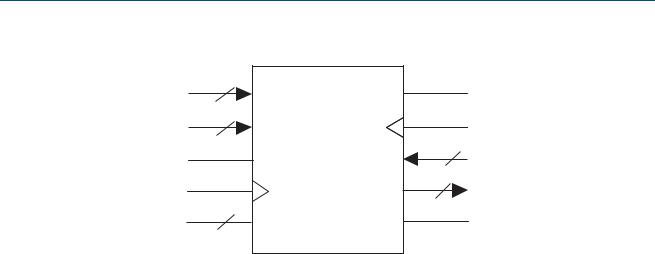
The QL4036 contains 672 logic cells and 14 Dual Port RAM modules (see Figure 1). Each RAM module has 1,152 RAM bits, for a total of 16,128 bits. RAM Modules are Dual Port (one read port, one write port) and can be configured into one of four modes:
64 (deep) × 18 (wide), 128 × 9, 256 × 4, or 512 × 2 (see Figure 4). With a maximum of 82 I/Os, the QL4036 is available in 144-pin TQFP, 208-pin PQFP, 208-pin CQFP, and 256pin PBGA packages.
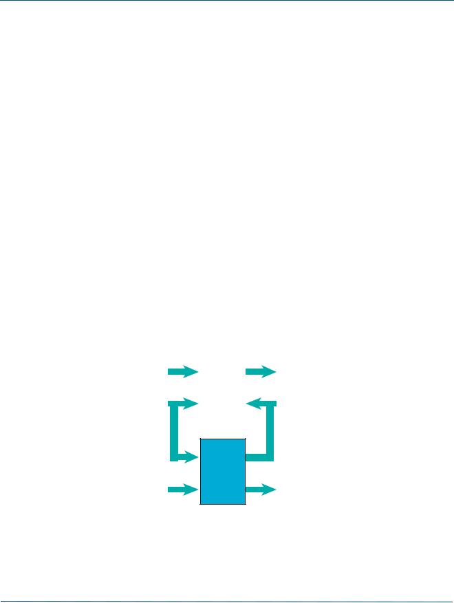
Designers can cascade multiple RAM modules to increase the depth or width allowed in single modules by connecting corresponding address lines together and dividing the words between modules (see Figure 2). This approach allows up to 512-deep configurations as large as 16 bits wide in the smallest QuickRAM device and 44 bits wide in the largest device.
Software support for the complete QuickRAM family, including the QL4036, is available through two basic packages. The turnkey QuickWorks TM package provides the most complete ESP software solution from design entry to logic synthesis, to place and route, to simulation. The QuickTools packages provides a solution for designers who use Cadence, Exemplar, Mentor, Synopsys, Synplicity, Viewlogic, Aldec, or other third-party tools for design entry, synthesis, or simulation.
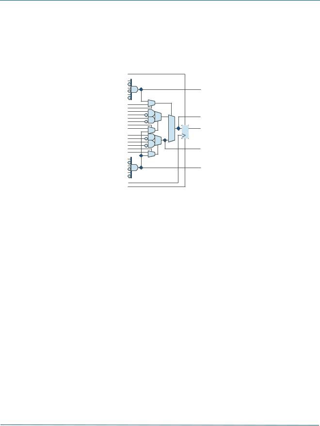
The QuickLogic TM variable grain logic cell features up to 16 simultaneous inputs and five outputs within a cell that can be fragmented into five independent cells. Each cell has a fanin of 29 including register and control lines (see Figure 3).
WDATA |
RAM |
RDATA |
|
Module |
|
|
(1,152 bits) |
|
WADDR |
|
RADDR |
|
|
|
RAM Module
(1,152 bits)
WDATA |
RDATA |
Figure 2: QuickRAM Module Bits
•
•
2 • www.quicklogic.com © 2002 QuickLogic Corporation
•
•
•

QL4036 QuickRAM Data Sheet Rev G
Product Summary
Total of 204 I/O Pins
•196 bi-directional input/output pins, PCI-compliant for 5.0 V and 3.3 V buses for -1/-2/-3/-4 speed grades
•8 high-drive input/distributed network pins
Eight Low-Skew Distributed Networks
•Two array clock/control networks available to the logic cell flip-flop clock, set and reset inputs—each driven by an input-only pin
•Six global clock/control networks available to the logic cell F1, clock, set and reset inputs and the input and I/O register clock, reset and enable inputs as well as the output enable control—each driven by an input-only or I/O pin, or any logic cell output or I/O cell feedback
High Performance Silicon
•Input + logic cell + output total delays = under 6 ns
•Data path speeds over 400 MHz
•Counter speeds over 300 MHz
•FIFO speeds over 160+ MHz
|
|
|
• |
© 2002 QuickLogic Corporation |
www.quicklogic.com |
• |
|
• 3 |
|||
|
|
|
• |
|
|
|
• |
|
|
|
• |
QL4036 QuickRAM Data Sheet Rev G
Electrical Specifications
AC Characteristics at VCC = 3.3 V, TA = 25°C (K = 1.00)
To calculate delays, multiply the appropriate K factor from Table 10: Operating Range by the following numbers in the tables provided.
QS |
|
|
A1 |
|
|
A2 |
|
|
A3 |
AZ |
|
A4 |
||
A5 |
|
|
A6 |
|
|
QS |
|
|
OP |
|
|
B1 |
|
|
B2 |
OZ |
|
C1 |
||
|
||
C2 |
|
|
MP |
QZ |
|
MS |
||
D1 |
|
|
D2 |
|
|
E1 |
|
|
E2 |
NZ |
|
NP |
||
NS |
|
|
F1 |
|
|
F2 |
|
|
F3 |
FZ |
|
F4 |
||
F5 |
|
|
F6 |
|
|
QC |
|
|
QR |
|
Figure 3: QuickRAM Logic Cell
Table 1: Logic Cell
Symbol |
Parameter |
|
|
Propagation Delays (ns) |
|
|
||||
|
|
|
Fanout (5) |
|
|
|
||||
|
|
|
|
|
|
|
|
|||
|
|
1 |
|
2 |
|
3 |
|
4 |
|
5 |
|
|
|
|
|
|
|||||
|
|
|
|
|
|
|
|
|
|
|
t |
Combinatorial Delaya |
1.4 |
|
1.7 |
|
1.9 |
|
2.2 |
|
3.2 |
PD |
|
|
|
|
|
|
|
|
|
|
t |
Setup Timea |
1.7 |
|
1.7 |
|
1.7 |
|
1.7 |
|
1.7 |
SU |
|
|
|
|
|
|
|
|
|
|
tH |
Hold Time |
0.0 |
|
0.0 |
|
0.0 |
|
0.0 |
|
0.0 |
|
|
|
|
|
|
|
|
|
|
|
tCLK |
Clock to Q Delay |
0.7 |
|
1.0 |
|
1.2 |
|
1.5 |
|
2.5 |
tCWHI |
Clock High Time |
1.2 |
|
1.2 |
|
1.2 |
|
1.2 |
|
1.2 |
tCWLO |
Clock Low Time |
1.2 |
|
1.2 |
|
1.2 |
|
1.2 |
|
1.2 |
tSET |
Set Delay |
1.0 |
|
1.3 |
|
1.5 |
|
1.8 |
|
2.8 |
tRESET |
Reset Delay |
0.8 |
|
1.1 |
|
1.3 |
|
1.6 |
|
2.6 |
tSW |
Set Width |
1.9 |
|
1.9 |
|
1.9 |
|
1.9 |
|
1.9 |
tRW |
Reset Width |
1.8 |
|
1.8 |
|
1.8 |
|
1.8 |
|
1.8 |
a.These limits are derived from a representative selection of the slowest paths through the QuickRAM logic cell including typical net delays. Worst case delay values for specific paths should be determined from timing analysis of your particular design.
•
•
4 • www.quicklogic.com © 2002 QuickLogic Corporation
•
•
•
QL4036 QuickRAM Data Sheet Rev G
[8:0] |
RE |
WA |
|
[17:0] |
RCLK |
WD |
|
WE |
[8:0] |
RA |
|
|
[17:0] |
WCLK |
RD |
[1:0] |
ASYNCRD |
MODE |
|
Figure 4: QuickRAM Module |
|
Table 2: RAM Cell Synchronous Write Timing
Symbol |
Parameter |
|
Propagation Delays (ns) |
|
|
|||
|
|
Fanout |
|
|
|
|
||
|
|
|
|
|
|
|
|
|
|
|
1 |
|
3 |
|
4 |
|
5 |
|
|
2 |
|
|
||||
|
|
|
|
|
|
|
|
|
tSWA |
WA Setup Time to WCLK |
1.0 |
1.0 |
1.0 |
|
1.0 |
|
1.0 |
tHWA |
WA Hold Time to WCLK |
0.0 |
0.0 |
0.0 |
|
0.0 |
|
0.0 |
tSWD |
WD Setup Time to WCLK |
1.0 |
1.0 |
1.0 |
|
1.0 |
|
1.0 |
tHWD |
WD Hold Time to WCLK |
0.0 |
0.0 |
0.0 |
|
0.0 |
|
0.0 |
tSWE |
WE Setup Time to WCLK |
1.0 |
1.0 |
1.0 |
|
1.0 |
|
1.0 |
tHWE |
WE Hold Time to WCLK |
0.0 |
0.0 |
0.0 |
|
0.0 |
|
0.0 |
t |
WCLK to RD (WA=RA)a |
5.0 |
5.3 |
5.6 |
|
5.9 |
|
7.1 |
WCRD |
|
|
|
|
|
|
|
|
a.Stated timing for worst case Propagation Delay over process variation at VCC = 3.3 V and
TA = 25°C. Multiply by the appropriate Delay Factor, K, for speed grade, voltage and temperature settings as specified in the Operating Range.
Table 3: RAM Cell Synchronous Read Timing
Symbol |
Parameter |
|
|
Propagation Delays (ns) |
|
|
||||
|
|
|
|
Fanout |
|
|
|
|
||
|
|
|
|
|
|
|
|
|
|
|
Logic Cells |
|
1 |
|
2 |
|
3 |
|
4 |
|
5 |
|
|
|
|
|
||||||
|
|
|
|
|
|
|
|
|
|
|
tSRA |
RA Setup Time to RCLK |
1.0 |
|
1.0 |
|
1.0 |
|
1.0 |
|
1.0 |
tHRA |
RA Hold Time to RCLK |
0.0 |
|
0.0 |
|
0.0 |
|
0.0 |
|
0.0 |
tSRE |
RE Setup Time to RCLK |
1.0 |
|
1.0 |
|
1.0 |
|
1.0 |
|
1.0 |
tHRE |
RE Hold Time to RCLK |
0.0 |
|
0.0 |
|
0.0 |
|
0.0 |
|
0.0 |
t |
RCLK to RDa |
4.0 |
|
4.3 |
|
4.6 |
|
4.9 |
|
6.1 |
RCRD |
|
|
|
|
|
|
|
|
|
|
a.Stated timing for worst case Propagation Delay over process variation at VCC = 3.3 V and
TA = 25°C. Multiply by the appropriate Delay Factor, K, for speed grade, voltage and temperature settings as specified in the Operating Range.
|
|
|
• |
© 2002 QuickLogic Corporation |
www.quicklogic.com |
• |
|
• 5 |
|||
|
|
|
• |
|
|
|
• |
|
|
|
• |

QL4036 QuickRAM Data Sheet Rev G
Table 4: RAM Cell Asynchronous Read Timing
Symbol |
|
Parameter |
|
Propagation Delays (ns) |
|
|
|||
|
|
|
Fanout |
|
|
|
|
||
|
|
|
|
|
|
|
|
|
|
|
|
|
1 |
|
3 |
|
4 |
|
5 |
|
|
|
2 |
|
|
||||
|
|
|
|
|
|
|
|
|
|
RPDRD |
RA to RDa |
|
3.0 |
3.3 |
3.6 |
|
3.9 |
|
5.1 |
|
|
|
|
|
|
|
|
|
|
a.Stated timing for worst case Propagation Delay over process variation at VCC = 3.3 V and
TA = 25°C. Multiply by the appropriate Delay Factor, K, for speed grade, voltage and temperature settings as specified in the Operating Range.
Table 5: Input-Only / Clock Cells
Symbol |
Parameter |
|
Propagation Delays (ns) |
|
|
|||||||
|
|
|
Fanout |
|
|
|
|
|
||||
|
|
|
|
|
|
|
|
|
|
|||
|
|
1 |
|
3 |
|
4 |
|
8 |
|
12 |
|
24 |
|
|
2 |
|
|
|
|
||||||
|
|
|
|
|
|
|
|
|
|
|
|
|
tIN |
High Drive Input Delay |
1.5 |
1.6 |
1.8 |
|
1.9 |
|
2.4 |
|
2.9 |
|
4.4 |
tINI |
High Drive Input, Inverting Delay |
1.6 |
1.7 |
.19 |
|
2.0 |
|
2.5 |
|
3.0 |
|
4.5 |
tISU |
Input Register Set-Up Time |
3.1 |
3.1 |
3.1 |
|
3.1 |
|
3.1 |
|
3.1 |
|
3.1 |
tIH |
Input Register Hold Time |
0.0 |
0.0 |
0.0 |
|
0.0 |
|
0.0 |
|
0.0 |
|
0.0 |
tICLK |
Input Register Clock To Q |
0.7 |
0.8 |
1.0 |
|
1.1 |
|
1.6 |
|
2.1 |
|
3.6 |
tIRST |
Input Register Reset Delay |
0.6 |
0.7 |
0.9 |
|
1.0 |
|
1.5 |
|
2.0 |
|
3.5 |
tIESU |
Input Register Clock Enable Setup Time |
2.3 |
2.3 |
2.3 |
|
2.3 |
|
2.3 |
|
2.3 |
|
2.3 |
tIEH |
Input Register Clock Enable Hold Time |
0.0 |
0.0 |
0.0 |
|
0.0 |
|
0.0 |
|
0.0 |
|
0.0 |
|
Table 6: Clock Cells |
|
|
|
|
|
|
|
|
|
|
|
|
|
|
|
|
|
|
|
|
|
|||
Symbol |
Parameter |
|
Propagation Delays (ns) |
|
|
|||||||
|
|
Fanouta |
|
|
|
|
||||||
|
|
|
|
|
|
|
|
|||||
|
|
1 |
2 |
3 |
|
4 |
|
8 |
|
10 |
|
11 |
|
|
|
|
|
|
|
|
|
|
|
|
|
tACK |
Array Clock Delay |
1.2 |
1.2 |
1.3 |
|
1.3 |
|
1.5 |
|
1.6 |
|
1.7 |
tGCKP |
Global Clock Pin Delay |
0.7 |
0.7 |
0.7 |
|
0.7 |
|
0.7 |
|
0.7 |
|
0.7 |
tGCKB |
Global Clock Buffer Delay |
0.8 |
0.8 |
0.9 |
|
0.9 |
|
1.1 |
|
1.2 |
|
1.3 |
a.The array distributed networks consist of 40 half columns and the global distributed networks consist of 44 half columns, each driven by an independent buffer. The number of half columns used does not affect clock buffer delay. The array clock has up to eight loads per half column. The global clock has up to 11 loads per half column.
•
•
6 • www.quicklogic.com © 2002 QuickLogic Corporation
•
•
•
 Loading...