


QUICK LOGIC QL3012-1PL84M, QL3012-0PL84M, QL3012-2PL84M, QL3025-2PQ208M, QL3040-0PQ208M Datasheet
...Military Plastic pASIC 3 Family
60,000 Usable PLD Gate pASIC3 FPGA Combining High Performance and High Density
Military pASIC 3 - 3.3V Family
DEVICE HIGHLIGHTS |
FEATURES |
Device Highlights |
Features |
|
High Performance and High Density
■60,000 Usable PLD Gates with 316 I/Os
■16-bit counter speeds over 300 MHZ, data path speeds over 400 MHz
■0.35um four-layer metal non-volatile CMOS process for smallest die sizes
Easy to Use/Fast Development Cycles
■100% routable with 100% utilization and complete pin-out stability
■Variable-grain logic cells provide high performance and 100% utilization
■Comprehensive design tools include high quality Verilog/VHDL synthesis
Advanced I/O Capabilities
■Interfaces with both 3.3 volt and 5.0 volt devices
■PCI compliant with 3.3V and 5.0V buses for -1/-2 speed grades
■Full JTAG boundary scan
■Registered I/O cells with individually controlled clocks and output enables
Total of 180 I/O pins
■308 bidirectional input/output pins, PCI-compliant for 5.0 volt and 3.3 volt buses for -1/-2 speed grades
■8 high-drive input/distributed network pins
Eight Low-Skew Distributed Networks
■Two array clock/control networks available to the logic cell flip-flop clock, set and reset inputs - each driven by an input-only pin
■Up to six global clock/control networks available to the logic cell F1, clock, set and reset inputs and the input and I/O register clock, reset and enable inputs as well as the output enable control - each driven by an input-only or I/O pin, or any logic cell output or I/O cell feedback
High Performance
■Input + logic cell + output total delays under 6 ns
■Data path speeds exceeding 400 MHz
■Counter speeds over 300 MHz
Device |
ASIC |
PLD |
Package |
Max |
Qualification |
Supply |
|
Gates |
Gates |
I/O |
Level |
Voltage |
|||
|
|
||||||
|
|
|
|
|
|
|
|
QL3012 |
8,000 |
12,000 |
84PLCC |
68 |
M |
3.3V |
|
QL3025 |
16,000 |
25,000 |
208PQFP |
174 |
M |
3.3V |
|
QL3040 |
24,000 |
40,000 |
208PQFP |
174 |
M |
3.3V |
|
QL3060 |
36,000 |
60,000 |
208PQFP |
174 |
M |
3.3V |
|
|
|
|
|
|
|
|
M = Military Temperature (-55 to +125 degrees C)
TABLE 1: Selector Table
Rev B |
8-23 |

Military Plastic pASIC 3 Family
PRODUCT SUMMARY
Product Summary
The pASIC 3 FPGA family features up to 60,000 usable PLD gates. pASIC 3 FPGAs are fabricated on a 0.35mm four-layer metal process using QuickLogic’s patented ViaLink technology to provide a unique combination of high performance, high density, low cost, and extreme ease-of-use.
The pASIC 3 product family contains 1,584 logic cells. With a maximum of 316 I/Os, and is available in 208-PQFP and 84-PLCC packages.
Software support for the complete pASIC 3 family is available through three basic packages. The turnkey QuickWorks® package provides the most complete FPGA software solution from design entry to logic synthesis, to place and route, to simulation. The QuickWorksTM-Lite and QuickToolsTM packages provide a solution for designers who use Cadence, Exemplar, Mentor, Synopsys, Synplicity, Viewlogic, Veribest, or other third-party tools for design entry, synthesis, or simulation.
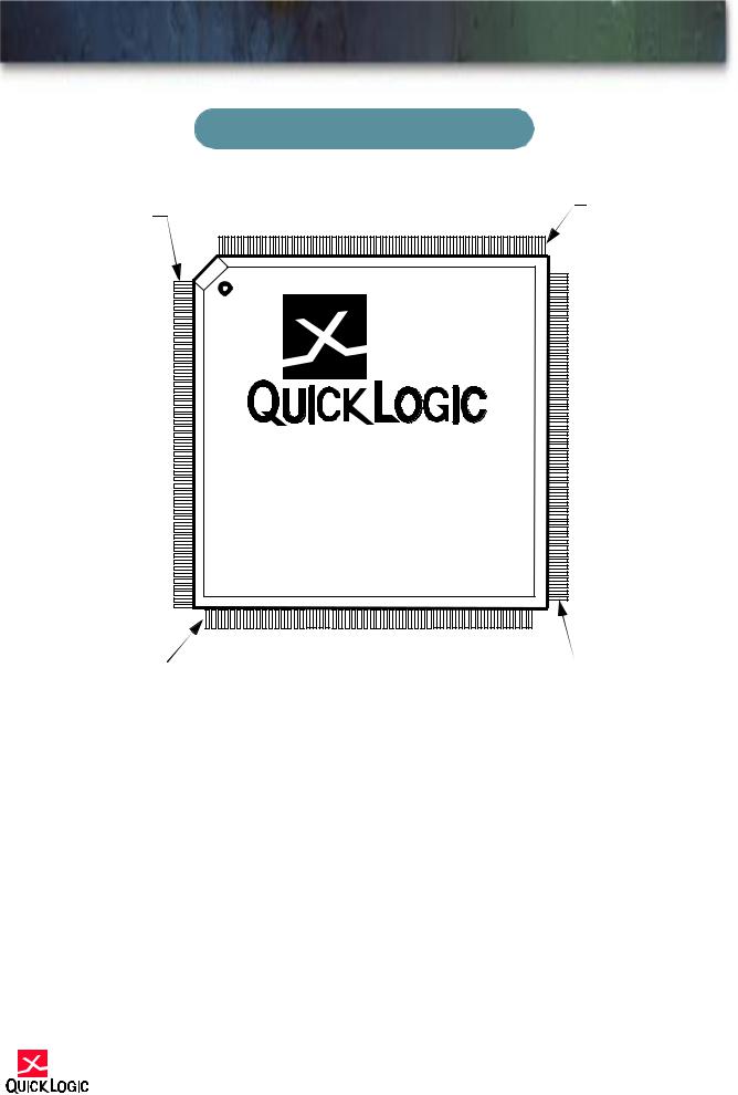
PINOUT DIAGRAM 84-PIN PLCC
Pinout Diagram 68-Pin CPGA
TABLE 2: 84-pin PLCC
8-24
24
Preliminary
Military Plastic pASIC 3 Family
PINOUT DIAGRAM 208-PIN PQFP
Pin #157
Pin #1
pASIC QL3060-1PQ208M
Pin #53 |
|
|
|
Pin #105 |
|
||||
|
|
8-25
Military Plastic pASIC 3 Family
PQFP 208-PINOUT TABLE
PQFP 208 Pinout Table
208 |
Function |
208 |
Function |
208 |
Function |
208 |
Function |
208 |
Function |
||||
PQFP |
|
|
PQFP |
|
|
PQFP |
|
|
PQFP |
|
|
PQFP |
|
208 |
I/O |
|
43 |
GND |
|
84 |
I/O |
|
125 |
I/O |
|
168 |
I/O |
1 |
I/O |
|
44 |
I/O |
|
85 |
I/O |
|
126 |
I/O |
|
169 |
I/O |
2 |
I/O |
|
45 |
I/O |
|
86 |
I/O |
|
127 |
GND |
|
NC |
I/O |
3 |
I/O |
|
46 |
I/O |
|
87 |
I/O |
|
128 |
I/O |
|
170 |
I/O |
4 |
I/O |
|
47 |
I/O |
|
88 |
I/O |
|
NC |
I/O |
|
171 |
I/O |
5 |
I/O |
|
48 |
I/O |
|
89 |
I/O |
|
129 |
GCLK / I |
|
172 |
I/O |
NC |
I/O |
|
NC |
I/O |
|
90 |
I/O |
|
130 |
ACLK / I |
|
173 |
I/O |
6 |
I/O |
|
49 |
I/O |
|
91 |
I/O |
|
131 |
VCC |
|
174 |
I/O |
7 |
I/O |
|
50 |
I/O |
|
92 |
I/O |
|
132 |
GCLK / I |
|
175 |
I/O |
8 |
I/O |
|
51 |
I/O |
|
NC |
I/O |
|
133 |
GCLK / I |
|
NC |
I/O |
9 |
I/O |
|
52 |
I/O |
|
93 |
I/O |
|
134 |
VCC |
|
176 |
I/O |
10 |
VCC |
|
53 |
I/O |
|
94 |
I/O |
|
135 |
I/O |
|
177 |
GND |
11 |
I/O |
|
54 |
TDI |
|
95 |
GND |
|
136 |
I/O |
|
178 |
I/O |
12 |
GND |
|
NC |
I/O |
|
96 |
I/O |
|
NC |
I/O |
|
179 |
I/O |
13 |
I/O |
|
NC |
I/O |
|
97 |
VCC |
|
137 |
I/O |
|
NC |
I/O |
14 |
I/O |
|
55 |
I/O |
|
98 |
I/O |
|
NC |
GND |
|
180 |
I/O |
NC |
I/O |
|
56 |
I/O |
|
99 |
I/O |
|
138 |
I/O |
|
181 |
I/O |
15 |
I/O |
|
NC |
I/O |
|
100 |
I/O |
|
139 |
I/O |
|
182 |
GND |
16 |
I/O |
|
57 |
I/O |
|
NC |
I/O |
|
140 |
I/O |
|
NC |
VCC |
17 |
I/O |
|
58 |
I/O |
|
101 |
I/O |
|
141 |
I/O |
|
183 |
I/O |
18 |
I/O |
|
59 |
GND |
|
NC |
I/O |
|
142 |
I/O |
|
184 |
I/O |
19 |
I/O |
|
60 |
I/O |
|
102 |
I/O |
|
NC |
I/O |
|
185 |
I/O |
20 |
I/O |
|
61 |
VCC |
|
NC |
I/O |
|
143 |
I/O |
|
186 |
I/O |
NC |
I/O |
|
62 |
I/O |
|
NC |
I/O |
|
144 |
I/O |
|
187 |
VCCIO |
21 |
I/O |
|
63 |
I/O |
|
103 |
TRSTB |
|
145 |
VCC |
|
188 |
I/O |
22 |
I/O |
|
64 |
I/O |
|
104 |
TMS |
|
NC |
I/O |
|
NC |
I/O |
23 |
GND |
|
NC |
I/O |
|
105 |
I/O |
|
146 |
I/O |
|
189 |
I/O |
24 |
I/O |
|
65 |
I/O |
|
NC |
I/O |
|
147 |
GND |
|
190 |
I/O |
25 |
GCLK / I |
|
66 |
I/O |
|
106 |
I/O |
|
148 |
I/O |
|
191 |
I/O |
26 |
ACLK / I |
|
67 |
I/O |
|
107 |
I/O |
|
149 |
I/O |
|
192 |
I/O |
27 |
VCC |
|
NC |
I/O |
|
108 |
I/O |
|
150 |
I/O |
|
193 |
I/O |
28 |
GCLK / I |
|
68 |
I/O |
|
109 |
I/O |
|
151 |
I/O |
|
194 |
I/O |
29 |
GCLK / I |
|
69 |
I/O |
|
NC |
I/O |
|
152 |
I/O |
|
NC |
I/O |
30 |
VCC |
|
70 |
I/O |
|
110 |
I/O |
|
153 |
I/O |
|
195 |
I/O |
31 |
I/O |
|
NC |
I/O |
|
111 |
I/O |
|
154 |
I/O |
|
196 |
I/O |
32 |
I/O |
|
71 |
I/O |
|
112 |
I/O |
|
155 |
I/O |
|
197 |
I/O |
NC |
GND |
|
NC |
I/O |
|
113 |
I/O |
|
156 |
I/O |
|
198 |
I/O |
33 |
I/O |
|
72 |
I/O |
|
114 |
VCC |
|
157 |
TCK |
|
NC |
I/O |
NC |
I/O |
|
73 |
GND |
|
115 |
I/O |
|
158 |
STM |
|
199 |
GND |
34 |
I/O |
|
74 |
I/O |
|
116 |
GND |
|
NC |
I/O |
|
200 |
I/O |
35 |
I/O |
|
NC |
VCC |
|
117 |
I/O |
|
159 |
I/O |
|
201 |
VCC |
36 |
I/O |
|
75 |
I/O |
|
NC |
I/O |
|
160 |
I/O |
|
202 |
I/O |
NC |
I/O |
|
76 |
I/O |
|
118 |
I/O |
|
161 |
I/O |
|
203 |
I/O |
37 |
I/O |
|
77 |
I/O |
|
119 |
I/O |
|
162 |
I/O |
|
204 |
I/O |
38 |
I/O |
|
78 |
GND |
|
120 |
I/O |
|
163 |
GND |
|
205 |
I/O |
39 |
I/O |
|
79 |
I/O |
|
121 |
I/O |
|
164 |
I/O |
|
206 |
I/O |
NC |
I/O |
|
80 |
I/O |
|
NC |
I/O |
|
165 |
VCC |
|
207 |
TDO |
40 |
I/O |
|
81 |
I/O |
|
122 |
I/O |
|
166 |
I/O |
|
|
|
41 |
VCC |
|
82 |
I/O |
|
123 |
I/O |
|
NC |
I/O |
|
|
|
42 |
I/O |
83 |
VCCIO |
124 |
I/O |
167 |
I/O |
|
|
|
|||
8-26
26 |
Preliminary |
Military Plastic pASIC 3 Family
ABSOLUTE MAXIMUM RATINGS
VCC Voltage........................... |
-0.5 to 4.6V |
VCCIO Voltage ....................... |
-0.5 to 7.0V |
Input Voltage.............. |
-0.5 to VCCIO+0.5V |
Latch-up Immunity .................. |
±200 mA |
DC Input Current ...................... |
±20 mA |
ESD Pad Protection .................... |
±2000V |
Storage Temperature ....... |
-65°C to +150°C |
Lead Temperature ........................... |
300°C |
OPERATING RANGE
Symbol |
Parameter |
|
|
Military |
|
Unit |
|
|
|
|
Min |
|
Max |
|
|
VCC |
Supply Voltage |
|
3.0 |
|
3.6 |
|
V |
VCCIO |
I/O Input Tolerance Voltage |
|
3.0 |
|
5.5 |
|
V |
TA |
Ambient Temperature |
|
-55 |
|
|
|
°C |
TC |
Case Temperature |
|
|
|
125 |
|
°C |
|
|
-0 Speed Grade |
0.42 |
|
2.03 |
|
|
K |
Delay Factor |
-1 Speed Grade |
0.42 |
|
1.64 |
|
|
|
|
-2 Speed Grade |
0.42 |
|
1.37 |
|
|
DC CHARACTERISTICS
Symbol |
Parameter |
Conditions |
Min |
Max |
Unit |
VIH |
Input HIGH Voltage |
|
0.5VCC |
VCCIO+0.5 |
V |
VIL |
Input LOW Voltage |
|
-0.5 |
0.3VCC |
V |
VOH |
Output HIGH Voltage |
IOH = -12 mA |
2.4 |
|
V |
|
|
IOH = -500 A |
0.9VCC |
|
V |
VOL |
Output LOW Voltage |
IOL = 8 mA [1] |
|
0.45 |
V |
|
|
IOL = 1.5 mA |
|
0.1VCC |
V |
II |
I or I/O Input Leakage Current |
VI = VCCIO or GND |
-10 |
10 |
A |
IOZ |
3-State Output Leakage Current |
VI = VCCIO or GND |
-10 |
10 |
A |
CI |
Input Capacitance [2] |
|
|
10 |
pF |
IOS |
Output Short Circuit Current [3] |
VO = GND |
-15 |
-180 |
mA |
|
|
VO = VCC |
40 |
210 |
mA |
ICC |
D.C. Supply Current [4] |
VI, VIO = VCCIO or GND |
0.50 (typ) |
5 |
mA |
ICCIO |
D.C. Supply Current on VCCIO |
|
0 |
100 |
A |
Notes:
[1]Military devices have 8 mA IOL specifications.
[2]Capacitance is sample tested only. Clock pins are 12 pF maximum.
[3]Only one output at a time. Duration should not exceed 30 seconds.
[4]Maximum ICC is 5 mA for all military grade devices. For AC conditions, contact QuickLogic customer engineering.
8-27
 Loading...