


ORDER NO.
RRV4374
X-EM21V
DVD Receiver System
X-EM21V
X-EM11V
THIS MANUAL IS APPLICABLE TO THE FOLLOWING MODEL(S) AND TYPE(S).
Model |
Type |
Power Requirement |
Region |
Remarks |
||||||||
No. |
||||||||||||
|
|
|
|
|
|
|
|
|
|
|
||
X-EM21V |
YXE8 |
AC 220 V to 240 V |
2 |
|
||||||||
X-EM21V |
LXE |
AC 220 V to 240 V |
3 |
|
||||||||
X-EM21V |
AXQ5 |
AC 220 V |
5 |
|
||||||||
X-EM11V |
AXQ5 |
AC 220 V |
5 |
|
||||||||
|
|
|
|
|
|
|
|
|
|
|
|
|
|
|
|
|
|
|
|
|
|
|
|
|
|
|
|
|
|
|
|
|
|
|
|
|
|
|
|
|
|
|
|
|
|
|
|
|
|
|
|
|
|
|
|
|
|
|
|
|
|
|
|
|
|
|
|
|
|
|
|
|
|
|
|
|
|
PIONEER CORPORATION 1-1, Shin-ogura, Saiwai-ku, Kawasaki-shi, Kanagawa 212-0031, Japan
PIONEER ELECTRONICS (USA) INC. P.O. Box 1760, Long Beach, CA 90801-1760, U.S.A.
PIONEER EUROPE NV Haven 1087, Keetberglaan 1, 9120 Melsele, Belgium
PIONEER ELECTRONICS ASIACENTRE PTE. LTD. 253 Alexandra Road, #04-01, Singapore 159936
 PIONEER CORPORATION 2012
K-MZV AUG. 2012 Printed in Japan
|
1 |
|
2 |
|
3 |
|
4 |
|
|
|
|
|
|
SAFETY INFORMATION
A
This service manual is intended for qualified service technicians; it is not meant for the casual do-it- yourselfer. Qualified technicians have the necessary test equipment and tools, and have been trained to properly and safely repair complex products such as those covered by this manual.
Improperly performed repairs can adversely affect the safety and reliability of the product and may void the warranty. If you are not qualified to perform the repair of this product properly and safely, you should not risk trying to do so and refer the repair to a qualified service technician.
WARNING
BThis product may contain a chemical known to the State of California to cause cancer, or birth defects or other reproductive harm.
Health & Safety Code Section 25249.6 - Proposition 65
|
|
|
|
|
|
|
|
|
|
|
|
|
|
|
|
|
|
|
|
|
|
|
|
|
|
|
|
|
|
|
|
|
|
|
|
|
|
|
|
|
|
|
|
|
|
|
|
|
|
|
|
|
|
|
|
|
|
|
|
|
|
|
|
|
|
|
|
|
|
|
|
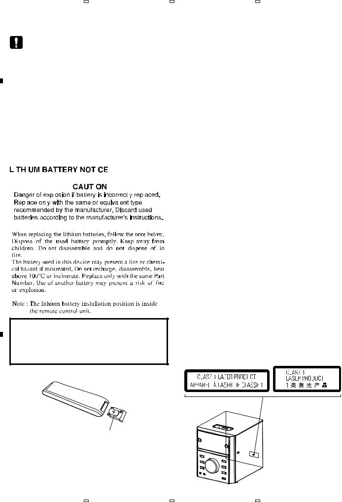
WARNING ! |
|
|
|
|
|
|
|
|
|
|
|
|
|
|
|
|
THE AEL (ACCESSIBLE EMISSION LEVEL) OF THE LASER POWER |
|||||
|
|
|
|
|
|
|
|
|
|
|
|
|||||||
|
|
|
|
|
|
|
|
|
|
|
|
|
OUTPUT IS LESS THAN CLASS 1 BUT THE LASER COMPONENT IS |
|||||
|
|
|
|
|
|
|
|
|
|
|
|
|
CAPABLE OF EMITTING RADIATION EXCEEDING THE LIMIT FOR |
|||||
|
|
|
|
|
|
|
|
|
|
|
|
|||||||
|
|
|
|
|
|
|
|
|
|
|
|
|
CLASS 1. |
|||||
|
|
|
|
|
|
|
|
|
|
|
|
|||||||
C |
|
|
|
|
|
|
|
|
|
|
|
A SPECIALLY INSTRUCTED PERSON SHOULD DO SERVICING |
||||||
|
|
|
|
|
|
|
|
|
|
|
|
|
OPERATION OF THE APPARATUS. |
|||||
|
|
|
|
|
|
|
|
|
|
|
|
|
|
|
|
|
|
|
|
|
|
|
|
|
|
|
|
|
|
|
|
|
|
|
|
|
|
|
|
|
|
|
|
|
|
|
|
|
|
|
|
LASER DIODE CHARACTERISTICS |
|
|
||
|
|
|
|
|
|
|
|
|
|
|
|
|
|
|
|
|||
|
|
|
|
|
|
|
|
|
|
|
|
|
FOR CD : MAXIMUM OUTPUT POWER : 5 mW |
|
||||
|
|
|
|
|
|
|
|
|
|
|
|
|
|
WAVELENGTH : 790 nm |
|
|||
|
|
|
|
|
|
|
|
|
|
|
|
|
FOR DVD : MAXIMUM OUTPUT POWER : 5 mW |
|
||||
|
|
|
|
|
|
|
|
|
|
|
|
|
|
|||||
|
|
|
|
|
|
|
|
|
|
|
|
|
|
WAVELENGTH : 655 nm |
|
|||
|
|
|
|
|
|
|
|
|
|
|
|
|
|
|
|
|
|
|
D
This product contains mercury. Disposal of this material may be regulated due to environmental considerations. For disposal or recycling information, please contact your local authorities or the Electronics Industries Alliance : www.eiae.org.
E |
Remote control |
|
|
|
|
|
|
|
LABEL CHECK
AXQ5 model
YXE8, LXE models
Battery (CR2025)
F
2 |
X-EM21V |
|
1 |
|
2 |
|
3 |
|
4 |
|
|
|
|
|
|

|
5 |
|
6 |
|
7 |
|
8 |
|
|
|
|
CONTENTS
SAFETY INFORMATION.......................................................................................................................................................... |
2 |
1. SERVICE PRECAUTIONS .................................................................................................................................................... |
4 |
1.1 NOTES ON SOLDERING ............................................................................................................................................... |
4 |
1.2 NOTES ON REPLACING THE MECHA ASSY............................................................................................................... |
4 |
2. SPECIFICATIONS................................................................................................................................................................. |
5 |
3. BASIC ITEMS FOR SERVICE .............................................................................................................................................. |
6 |
3.1 CHECK POINTS AFTER SERVICING ........................................................................................................................... |
6 |
3.2 JIGS LIST ....................................................................................................................................................................... |
6 |
3.3 PCB LOCATIONS ........................................................................................................................................................... |
7 |
4. BLOCK DIAGRAM ................................................................................................................................................................ |
8 |
4.1 OVERALL WIRING DIAGRAM ....................................................................................................................................... |
8 |
4.2 OVERALL BLOCK DIAGRAM....................................................................................................................................... |
10 |
5. DIAGNOSIS ........................................................................................................................................................................ |
12 |
5.1 TROUBLESHOOTING.................................................................................................................................................. |
12 |
5.2 HOW TO EVALUATE LD DETERIORATION OF PICKUP ASSY.................................................................................. |
19 |
5.3 PROTECTION CIRCUIT............................................................................................................................................... |
20 |
5.4 IC INFORMATION ........................................................................................................................................................ |
21 |
6. SERVICE MODE ................................................................................................................................................................. |
21 |
7. DISASSEMBLY ................................................................................................................................................................... |
22 |
8. EACH SETTING AND ADJUSTMENT ................................................................................................................................ |
25 |
8.1 NECESSARY ITEMS TO BE NOTED........................................................................................................................... |
25 |
8.2 SPECIAL KEY FUNCTION SPECIFICATIONS ............................................................................................................ |
25 |
8.3 UPDATING OF THE FIRMWARE (MAIN MICROCOMPUTER) ................................................................................... |
25 |
8.4 UPDATING OF THE FIRMWARE (DVD MICROCOMPUTER) ..................................................................................... |
26 |
9. EXPLODED VIEWS AND PARTS LIST............................................................................................................................... |
28 |
9.1 PACKING SECTION ..................................................................................................................................................... |
28 |
9.2 EXTERIOR SECTION .................................................................................................................................................. |
30 |
10. SCHEMATIC DIAGRAM.................................................................................................................................................... |
32 |
10.1 MAIN ASSY (1/8)........................................................................................................................................................ |
32 |
10.2 MAIN ASSY (2/8)........................................................................................................................................................ |
34 |
10.3 MAIN ASSY (3/8)........................................................................................................................................................ |
36 |
10.4 MAIN ASSY (4/8)........................................................................................................................................................ |
38 |
10.5 MAIN ASSY (5/8)........................................................................................................................................................ |
40 |
10.6 MAIN ASSY (6/8)........................................................................................................................................................ |
42 |
10.7 MAIN ASSY (7/8)........................................................................................................................................................ |
44 |
10.8 MAIN ASSY (8/8)........................................................................................................................................................ |
46 |
10.9 iPOD, USB and AUX ASSYS...................................................................................................................................... |
48 |
10.10 DISPLAY LCD and VOL ASSYS............................................................................................................................... |
50 |
10.11 SMPS ASSY ............................................................................................................................................................. |
52 |
11. PCB CONNECTION DIAGRAM ........................................................................................................................................ |
54 |
11.1 MAIN ASSY ................................................................................................................................................................ |
54 |
11.2 iPOD, USB, AUX, DISPLAY LCD and VOL ASSYS.................................................................................................... |
56 |
11.3 SMPS ASSY ............................................................................................................................................................... |
58 |
A
B
C
D
E
F
X-EM21V |
3 |
|
5 |
|
6 |
|
7 |
|
8 |
|
|
|
|
|
|
|
1 |
|
2 |
|
3 |
|
4 |
|
|
|
|
|
|
1. SERVICE PRECAUTIONS
1.1 NOTES ON SOLDERING
A • For environmental protection, lead-free solder is used on the printed circuit boards mounted in this unit.
Be sure to use lead-free solder and a soldering iron that can meet specifications for use with lead-free solders for repairs accompanied by reworking of soldering.
•Compared with conventional eutectic solders, lead-free solders have higher melting points, by approximately 40 ºC. Therefore, for lead-free soldering, the tip temperature of a soldering iron must be set to around 373 ºC in general, although
the temperature depends on the heat capacity of the PC board on which reworking is required and the weight of the tip of the soldering iron.
Do NOT use a soldering iron whose tip temperature cannot be controlled.
Compared with eutectic solders, lead-free solders have higher bond strengths but slower wetting times and higher melting
Btemperatures (hard to melt/easy to harden).
The following lead-free solders are available as service parts:
•Parts numbers of lead-free solder: GYP1006 1.0 in dia.
GYP1007 0.6 in dia. GYP1008 0.3 in dia.
C
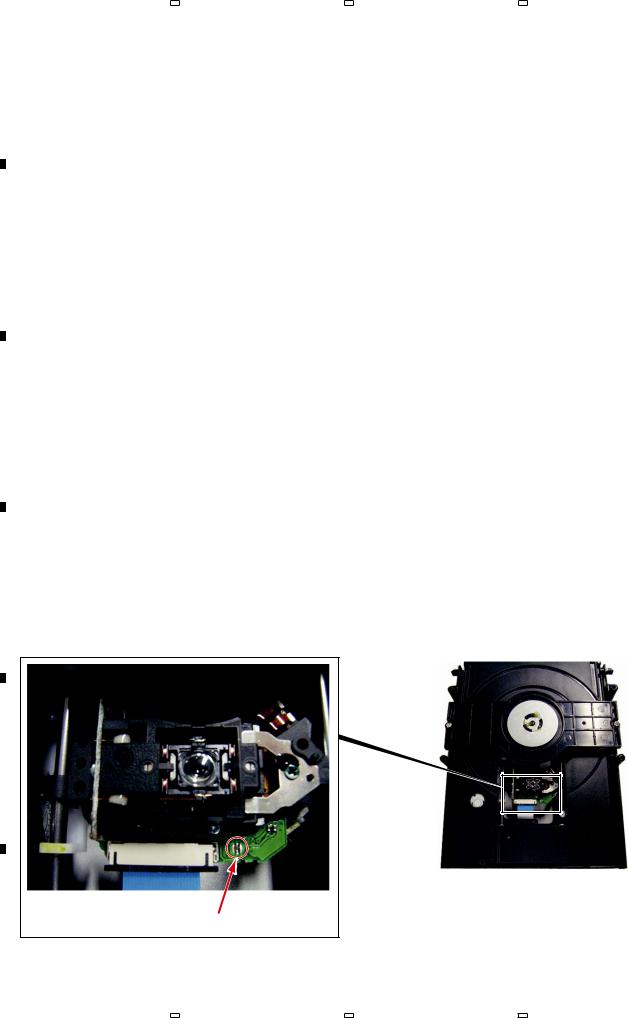
1.2 NOTES ON REPLACING THE MECHA ASSY
D
During replacement of the MECHA Assy, check the short-circuiting point indicated in the photo below. If it is short-circuited with solder, be sure to remove the solder.
Be careful of electrostatic discharge during connection of the FFC, because it may damage the Laser diode.
E
The short point of the solder
F
4 |
X-EM21V |
|
1 |
|
2 |
|
3 |
|
4 |
|
|
|
|
|
|

|
5 |
|
6 |
|
|
2. SPECIFICATIONS
• Amplifier
Rated Output Power ... 10 W + 10 W, RMS, 1 kHz, 8 Ω, 10%
• Disc |
|
|
Video Decoding |
........................... |
MPEG-1 / MPEG-2 / DivX |
Signal System.................................................... |
|
PAL / NTSC |
Video Format ......................................................... |
|
4:3 / 16:9 |
• Tuner (FM) |
|
|
Tuning range....................................... |
|
87.5 MHz to 108 MHz |
• Speakers |
|
8 Ω |
Speaker Impedance ........................................................ |
||
Speaker Driver.................................... |
|
101.6 mm, Full range |
• General information |
|
|
AC power............ |
220 V to 240 V , 50 Hz/60 Hz (YXE8, LXE) |
|
|
|
220 V, 50 Hz (AXQ5) |
Operation power ....................consumption |
28 W(X-EM21V) |
|
|
|
18 W(X-EM11V) |
Standby power consumption .................................... |
≤ 0.6 W |
|
USB Direct.................................... |
|
USB 1.1/2.0 (Full Speed) |
Dimensions |
|
|
–Main unit (W x H x D) .......152 mm x 175 mm x 215 mm
–Speaker box (W x H x D)..135 mm x 175 mm x 198 mm Weight
– With packing |
.............................................................5.3 kg |
– Main unit................................................................. |
1.36 kg |
– Speaker box ..................................................... |
1.33 kg x 2 |
Note
•The specifications and design of this product are subject to change without notice.
•Corporation and product names mentioned herein are trademarks or registered trademarks of the respective corporations.
|
7 |
|
8 |
|
|
 Accessories
• AC power cord
(SYXE8: 151-230230-002) (CMXE: 151-117117-701)
• Remote control
(SYXE8: RC34-X010XX-010) (CMXE: RC32-X020XX-220)
•Warranty card
•Operating Instructions
(SYXE8: 601-EM1100-010, 601-EM2100-010) (CMXE: 601-EM2100-010)
A
B
C
D
E
F
X-EM21V |
5 |
|
5 |
|
6 |
|
7 |
|
8 |
|
|
|
|
|
|
|
1 |
|
2 |
|
3 |
|
4 |
|
|
|
|
|
|
3. BASIC ITEMS FOR SERVICE
3.1 CHECK POINTS AFTER SERVICING
A Items to be checked after servicing
To keep the product quality after servicing, confirm recommended check points shown below.
|
|
No. |
Procedure |
Check points |
|
|
|
|
|
|
|
1 |
Confirm whether the customer complain has been solved. |
The customer complain must not be reappeared. |
|
|
|
|
Audio and operations must be normal. |
|
|
|
|
|
|
|
2 |
Check the DVD playback. |
Video, audio and operations (search etc.) must be normal. |
|
||||
|
|
|
|
|
|
|
3 |
Check the CD playback. |
Audio and operations (search etc.) must be normal. |
|
|
|
|
|
|
|
4 |
Check the USB playback. |
Audio and operations must be normal. |
|
|
|
|
|
|
|
5 |
Check the tuner operations. |
Audio and operations (station search etc.) must be normal. |
|
|
|
|
|
B |
6 |
Check the external input playback. |
Audio and operations must be normal. |
|
|
|
|
||
|
7 |
Check the appearance of the product. |
No scratches or dirt on its appearance after receiving it |
|
|
|
|
|
for service. |
See the table below for the items to be checked regarding video and audio.
|
|
Item to be checked regarding video |
Item to be checked regarding audio |
|
|
||
|
|
|
|
|
|
Block noise |
Distortion |
|
|
|
|
|
|
Horizontal noise |
Noise |
|
|
|
|
|
|
Dot noise |
Volume too low |
C |
|
|
|
Disturbed image (video jumpiness) |
Volume too high |
||
|
|
|
|
|
|
Too dark |
Volume fluctuating |
|
|
|
|
|
|
Too bright |
Sound interrupted |
|
|
|
|
|
|
Mottled color |
|
|
|
|
|
|
|
|
|
D3.2 JIGS LIST
 Jigs List
|
Jig Name |
|
Part No. |
Remarks |
|
Speaker cable connection jig |
|
GGD1814 |
Diagnosis |
|
Lubricants and Glues List |
|
|
|
|
Name |
Part No. |
|
Remarks |
E |
Bond |
GYA1011 |
Refer to "9.2 EXTERIOR SECTION". |
|
|
||||
|
|
|
Be for antenna cord suspension. Anything is enough for the bond, |
|
|
|
|
but consider a case to replacing the antenna cord. |
|
|
|
|
Recommend silicon bond (GYA1011). |
|
 Cleaning
Before shipping out the product, be sure to clean the following positions by using the prescribed cleaning tools.
|
Position to be cleaned |
Name |
|
Part No. |
|
Remarks |
F |
Pickup lens |
Cleaning liquied |
|
GEM1004 |
|
Refer to "7. DISASSEMBLY". |
|
|
|
|
|
|
|
|
|
Cleaning paper |
|
GED-008 |
|
|
|
|
|
|
|
|
|
6 |
|
|
|
|
|
|
|
|
X-EM21V |
|
|
||
|
|
|
|
|
|
|
|
1 |
|
2 |
|
3 |
|
4 |
|
|
|
|
|
|
|
5 |
|
6 |
|
7 |
|
8 |
|
|
|
|
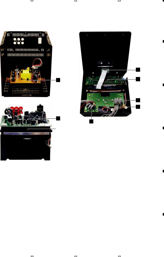
3.3 PCB LOCATIONS
G
A
SMPS ASSY
MAIN ASSY
Note:
This photo is X-EM21V. The iPod dock is not equipped with in X-EM11V.
• Rear view
B iPOD ASSY (X-EM21V only)
E DISPLAY LCD
ASSY
F VOL ASSY
D AUX ASSY
C USB ASSY
MECHA ASSY
NOTES: - Parts marked by “NSP” are generally unavailable because they are not in our Master Spare Parts List.
-The > mark found on some component parts indicates the importance of the safety factor of the part. Therefore, when replacing, be sure to use parts of identical designation.
Mark No. Description |
Part No. |
Mark No. Description |
|
Part No. |
|||
|
|
|
|
|
|
|
|
LIST OF ASSEMBLIES
1..MAIN ASSY (X-EM21V/YXE8) 1..MAIN ASSY (X-EM21V/LXE) 1..MAIN ASSY (X-EM21V/AXQ5) 1..MAIN ASSY (X-EM11V/AXQ5)
1..iPOD ASSY (X-EM21V ONLY)
1..USB ASSY (X-EM21V)
1..USB ASSY (X-EM11V) 1..DISPLAY LCD ASSY (X-EM21V) 1..DISPLAY LCD ASSY (X-EM11V)
X-EM21V-02800-00-E X-EM21V-02800-00-A X-EM21V-02800-00-C X-EM11V-02800-00-C
X-EM21V-07800-00
X-EM21V-06800-00 X-EM11V-06800-00 X-EM21V-03800-00 X-EM11V-03800-00
1..AUX ASSY (X-EM21V) |
X-EM21V-05800-00 |
1..AUX ASSY (X-EM11V) |
X-EM11V-05800-00 |
1..VOL ASSY (X-EM21V) |
X-EM21V-04800-00 |
1..VOL ASSY (X-EM11V) |
X-EM11V-04800-00 |
1..SMPS ASSY (X-EM21V) |
X-EM21V-12800-69 |
1..SMPS ASSY (X-EM11V) |
X-EM11V-12800-69 |
MECHA ASSY |
EM2-100002-356 |
X-EM21V |
7 |
A
B
C
D
E
F
|
5 |
|
6 |
|
7 |
|
8 |
|
|
|
|
|
|
|
1 |
|
2 |
|
|
4. BLOCK DIAGRAM
4.1 OVERALL WIRING DIAGRAM
A
B
C
F
VOL ASSY
(X-EM21V: X-EM21V-04800-00) (X-EM11V: X-EM11V-04800-00)
E
DISPLAY LCD ASSY (X-EM21V: X-EM21V-03800-00) (X-EM11V: X-EM11V-03800-00)
CN804 |
1.VOL- 2.VOL+ 3.AD-KEY 4.GND |
4 |
CN802
*1.00mm
CN801
C |
|
|
USB ASSY |
|
|
(X-EM21V: X-EM21V-06800-00) |
CN503 |
|
(X-EM11V: X-EM11V-06800-00) |
||
|
D
CN504
D
AUX ASSY
E
(X-EM21V: X-EM21V-05800-00) (X-EM11V: X-EM11V-05800-00)
CN506
|
3 |
|
4 |
|
A  A 1/8- A 8/8
MAIN ASSY
(X-EM21V/YXE8: X-EM21V-02800-00 (X-EM21V/LXE: X-EM21V-02800-00-A (X-EM21V/AXQ5: X-EM21V-02800-00 (X-EM11V/AXQ5: X-EM11V-02800-00
|
|
|
|
|
|
|
|
1 |
.KEY |
235-110080-210 |
|
|
|
2.VOL- |
|||||
|
|
|
|
|
|
|
|
3 |
.VLO+ |
|
|
|
|
|
|
|
|
4 |
.IR |
|
|
11/80 |
|
|
|
|
|
5 |
.LCD+5V |
|
|
|
|
|
|
m |
6.CD-VDD |
||
|
|
|
|
|
|
||||
|
|
|
|
|
|
|
7 |
.GND |
|
|
|
*1.00mm |
|
|
|
|
0m |
||
|
|
|
|
|
|
8 |
.LCD-DA |
||
|
|
|
|
|
|
|
1.0 |
||
|
|
|
|
|
|
|
9.LCD-WR |
||
|
|
|
|
|
|
||||
|
|
|
|
|
* |
10.LCD-CS |
|||
|
|
|
|
|
CN703 |
||||
|
|
|
|
|
11.PWR-EN |
||||
|
|
XP906 |
|
|
|
|
|
|
|
|
|
1 |
.USB+5V |
|
|
|
|
|
|
|
|
|
|
|
|
|
|
||
4 |
|
2 |
.D- |
|
|
|
|
|
|
|
3 |
.D+ |
|
|
|
|
|
|
|
|
|
|
|
|
|
|
|
||
|
|
4 |
.U-GND |
|
|
|
|
|
|
|
|
CN403 |
|
|
|
|
|
|
|
|
|
1 |
.GND |
|
|
|
|
|
|
2 |
|
|
|
|
|
|
|
||
|
|
2 |
.GND |
|
|
|
|
|
|
|
|
CN501 |
|
|
|
|
|
|
|
|
|
1 |
.AUX-L |
|
|
|
|
|
|
|
|
|
|
|
|
|
|
||
|
|
|
|
|
|
|
|
||
|
|
2 |
.GND |
|
|
|
|
|
|
|
|
3 |
.AUX-R |
|
|
|
|
|
|
8 |
|
4 |
.AUX-DET |
1.12V 2.12V 3.GND 4.GDN |
CN402 |
||||
|
7 |
.HP-L |
|||||||
|
|
5 |
.HP-DET |
|
|
|
|
|
|
|
|
6 |
.HP-R |
|
|
|
|
|
|
|
|
8 |
.GND |
|
|
|
|
|
|
|
|
|
|
4 |
|
|
|
||
|
|
|
|
|
|
|
|
|
|
G
SMPS ASSY
F (X-EM21V: X-EM21V-12800-69)
(X-EM11V: X-EM11V-12800-69)
8 |
X-EM21V |
CN1102
|
1 |
|
2 |
|
3 |
|
4 |
|
|
|
|
|
|
5
V-02800-00-E) 02800-00-A) V-02800-00-C) V-02800-00-C)
4.GDN |
CN402 |
||
|
|
|
|
|
|
|
|
CN1102
|
|
6 |
|
7 |
8 |
|
|
|
|
|
|
|
A |
|
|
|
|
|
MECHA ASSY |
|
|
|
|
|
|
(EM2-100002-356) |
|
|
|
CN701 |
|
|
|
|
|
|
1.M+ |
|
|
|
|
|
|
2.M- |
|
|
|
|
|
|
3.OP-SW |
5 |
|
5 |
|
|
|
4.GND |
|
|
|
|
|
|
5.CL-SW |
|
|
|
|
|
|
|
|
|
|
B |
|
|
XP902 |
|
|
|
|
|
|
1.SL+ |
|
|
|
|
|
|
2.SL- |
|
|
|
|
|
|
3.LIMIT |
6 |
|
|
|
|
|
4.GND |
|
|
|
|
|
|
|
|
|
|
|
1.F+ |
5.SP+ |
|
|
|
|
|
6.SP- |
|
|
|
|
||
2.F- |
|
|
|
|
||
|
|
|
|
|
||
3.T+ |
|
|
|
|
|
|
4.T- |
|
|
|
|
|
|
5.C |
|
|
|
|
|
|
6.D |
|
|
|
|
|
|
7.LDSW |
|
|
|
|
|
|
8.RFO |
CN902 |
|
|
|
C |
|
9.A |
|
|
|
|
|
|
10 |
.B |
|
|
|
|
|
11 |
.F |
|
|
24 |
0*.50mm |
|
12 |
.RFGND |
|
|
|
||
13 |
.VREF_OPU |
|
|
|
||
14 |
.A+5V |
mm.0*50 |
|
*0.50mm |
|
|
|
|
|
|
|||
15 |
.E |
|
|
|
|
|
16 |
.RFGND |
|
|
|
|
|
17 |
.VR_CD |
|
|
|
|
|
18 |
.VR_DVD |
|
|
|
|
|
19 |
.PUH_CDLD |
|
|
|
|
|
20 |
.MDI |
|
|
|
|
|
21 |
.A+5V |
|
|
|
|
|
22 |
.RFGND |
|
|
|
|
|
23 |
.PUH_DVDLD |
|
|
|
D |
|
24 |
.RFGND |
|
|
|
|
|
|
|
|
|
|
X-EM21V ONLY |
|
|
|
|
|
|
B iPOD ASSY |
|
1.IPOD+5V |
|
|
|
(X-EM21V-07800-00) |
|
|
2.IPOD+5V |
|
|
|
|
|
|
3.IPOD+5V |
|
|
235-140150-110 |
|
|
|
4.GND |
CN601 |
|
CN602 |
|
||
5.GND |
|
|
|
|
|
|
6.GND |
|
|
|
|
|
|
7.IPOD_TX |
|
|
14/80 |
|
|
|
8.IPOD_RX |
|
|
1*.00mm |
E |
||
9.IPOD_DET30 |
|
|
|
|||
|
|
1*.mm00 |
|
*1.00mm |
|
|
10.IPOD_DET13 |
|
|
|
|||
11.IPOD_IO |
|
|
|
|
|
|
12.AUDIO_Rch |
|
|
|
|
||
13.AUDIO_Lch |
|
|
|
|
||
14.AUDIO_RETURN |
|
|
|
|
||
|
|
|
|
|
|
F |
-When ordering service parts, be sure to refer to "EXPLODED VIEWS and PARTS LIST" or "PCB PARTS LIST".
-The > mark found on some component parts indicates the importance of the safety factor of the part. Therefore, when replacing, be sure to use parts of identical designation.
X-EM21V |
9 |
|
5 |
|
6 |
|
7 |
|
8 |
|
|
|
|
|
|

|
1 |
|
2 |
|
3 |
|
4 |
|
|
|
|
|
|
A
B
C
4.2 OVERALL BLOCK DIAGRAM
A MAIN ASSY
D
AUX ASSY
IC503
B |
|
iPOD ASSY |
IC602 |
(X-EM21V only)
IC101
32.768 kHz
IC701
E |
|
|
DISPLAY LCD |
LCD801 |
IC801 |
ASSY |
|
|
IC504
IC703
D |
IC704 |
|
U901 |
|
IC702 |
E |
U903 |
|
MECHA ASSY
F |
U904 |
U905 |
|
|
10 |
X-EM21V |
|
1 |
|
2 |
|
3 |
|
4 |
|
|
|
|
|
|
|
5 |
|
6 |
|
7 |
|
8 |
|
|
|
|
|
|
A
D AUX ASSY
IC504
IC501
IC601
B
X-EM21V only
|
|
|
|
|
|
|
|
|
|
|
|
|
|
|
|
|
|
|
|
|
|
|
|
|
|
|
|
|
|
|
|
|
|
|
|
|
|
|
|
|
|
|
|
|
|
|
|
|
|
|
|
|
|
|
|
|
|
|
|
|
|
|
|
|
|
|
|
|
|
|
|
|
|
|
|
|
|
|
|
|
|
|
|
|
|
|
|
U907 |
|
|
|
|
IC302 |
|
|||||||||||||||
|
|
|
|
|
|
|
|
|
|
|
|
|
|
|
|
|
|
|
|||
C
IC703
U906
IC704 |
D |
|
U901
E
G SMPS ASSY
U905 |
F |
|
X-EM21V |
11 |
|
5 |
|
6 |
|
7 |
|
8 |
|
|
|
|
|
|

|
1 |
|
2 |
|
3 |
|
4 |
|
|
|
|
|
|
5. DIAGNOSIS
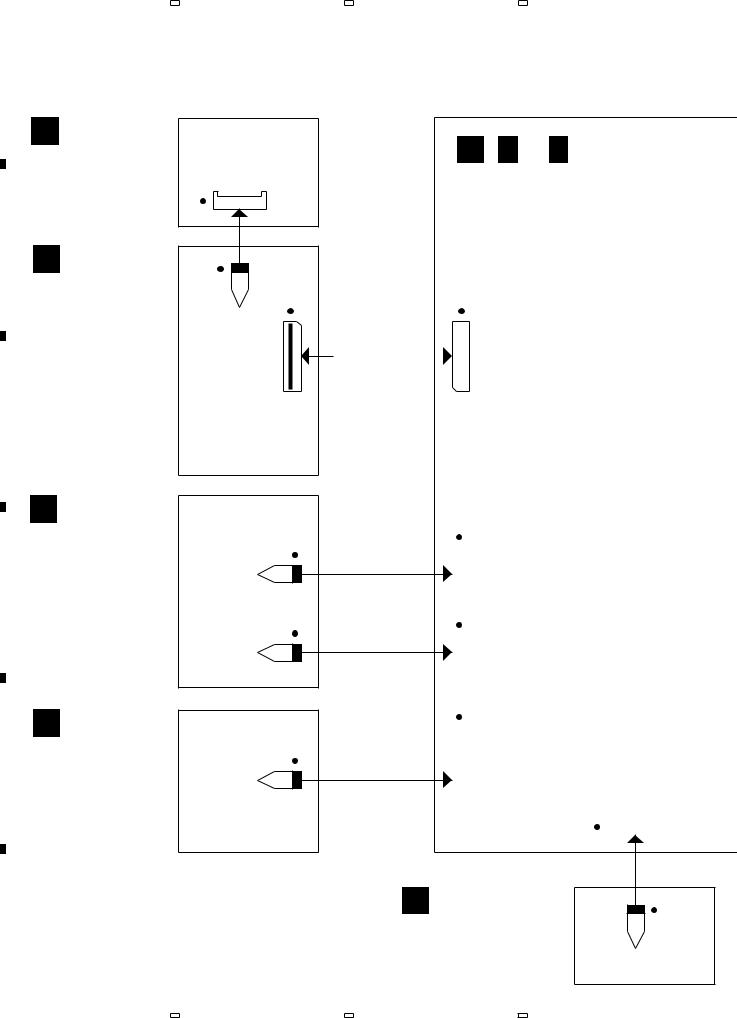
5.1 TROUBLESHOOTING
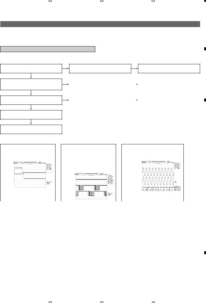
A[1] Operations with a DVD or CD not possible
1.Focus RF system check
2.Tracking system check
3.Spindle motor system check
4.Miscellaneous
1. Focus RF system check
After a DVD or CD is placed, the tray can be closed, but "NO DISC" is displayed.
1.Can the pickup be moved to the inner track of the disc?
B
Yes
2.Can the focus lens move up or down? (See the waveforms in Fig. 1.)
Yes
3. Is the laser diode lit?
Yes
4. Can the spindle motor turn?
No Check the voltage of the sled motor at Pins 3 and 4 of CN904.
Check the peripheral circuits of the focus lens,
No specifically the communication (FOCUS) lines between Pin 111 of U901 and Pin 1 of U903 and Pins 13 and 14 of U903 and Pins 1 and 2 of CN902.
No Check the peripheral circuit of the Q909 (CD), Q910 (DVD) laser diode drivers.
No
The spindle motor is in failure.
If the voltages does not appear, replace the MAIN Assy.
If the waveforms are not proper, replace the MAIN Assy.
If the waveforms from B and C of Q909, Q910 are not proper, replace the MAIN Assy.
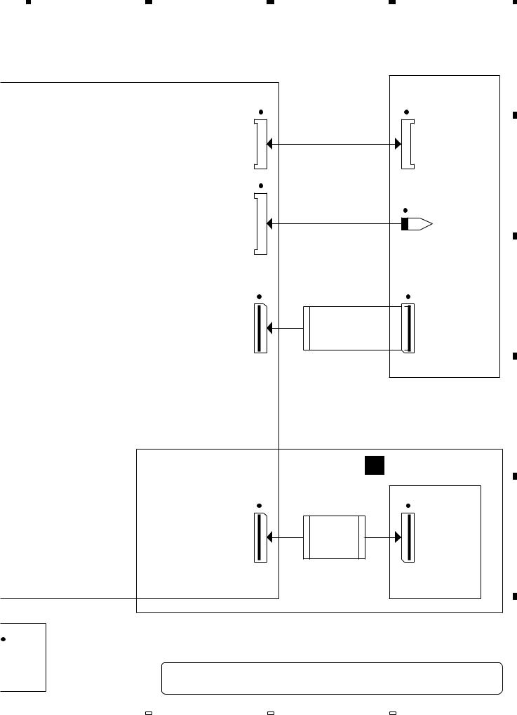
C
A disc can be loaded, but playback does not start.
1.Has the focus servo started? (See the waveforms in Fig. 2.)
Yes
2.Are the RF waveforms normal? (See the waveforms in Fig. 3.)
|
No |
Check Pins 110 and 111 of U901; Pins 13, 14, |
|
|
|
|
|
|
|
|
|||
|
15, and 16 of U903; and the peripheral circuit of |
|
|
Replace the MAIN Assy. |
||
|
|
|
|
|
||
|
|
|
the Q909, Q910 laser diode drivers. |
|
|
|
|
No |
|
|
|
|
|
|
|
|
|
|
||
|
If the level of the waveform is not normal, the |
|
|
|
||
|
|
|
MECHA Assy may be defective. |
|
|
|
|
|
|
|
|
|
|
|
1 |
U901 - pin 111 (FOSO) |
|
1 |
U901 |
- pin 111 (FOSO) |
|
4 U901 - pin 92 (RFO) |
|
|
|
|
|
V: 0.2 V/div. H: 1 s/div. |
|
|
V: 0.2 V/div. H: 1 s/div. |
|
[CD] |
[DVD] |
|
D |
2 |
U901 - pin 110 (TRSO) |
|
3 |
U901 |
- pin 92 (RFO) |
|
|||
|
|
V: 0.2 V/div. H: 0.1 μs/div. |
V: 0.5 V/div. H: 0.1 μs/div. |
|||||||
|
|
|
V: 0.1 V/div. H: 1 s/div. |
|
|
V: 1 V/div. H: 1 s/div. |
|
|||
|
|
|
|
|
|
|
|
|||
|
1 |
|
|
1 |
|
|
|
4 |
4 |
|
|
|
|
|
|
|
|
|
|
||
|
2 |
|
|
3 |
|
|
|
|
|
|
|
|
|
|
|
|
|
|
|
||
|
|
|
|
|
|
|
||||
|
|
|
|
|
|
|
|
|
|
|
|
|
Fig. 1 Waveform |
Fig. 2 Waveform |
Fig. 3 Waveform |
|||||||
E |
|
|
|
|
|
|
|
|
|||
|
|
|
|
|
|
|
|
|
|
|
|
|
|
2. Tracking system check |
|
|
|
|
|
|
|
|
|
|
|
|
|
|
|
|
|
|
|
|
|
|
|
|
|
|
Yes |
The tracking servo is not functioning. Check |
|
|
|||
|
|
1. Is "NO DISC" displayed immediately after the |
|
Pin 110 of U901; Pins 26, 15, 16 of U903; |
|
|
Replace the MAIN Assy. |
||||
|
|
tray is closed? |
|
|
|
|
|
||||
|
|
|
|
|
and the peripheral circuit of CN902. |
|
|
|
|||
|
|
|
|
|
|
|
|
|
|||
|
|
|
No |
|
|
|
|
|
|
|
|
|
|
|
|
|
|
|
|
|
|
||
|
|
|
|
|
|
|
|
|
|
|
|
2. Playback does not start although the TOC can Yes be read.
No
F
Yes
3. The TOC cannot be read.
A normal jump command cannot be completed, or the
beginning of a track cannot be found. Check the  Replace the MAIN Assy. peripheries of Pin 111 of U901 and Pin 26 of U903.
U901 is defective. |
|
|
Replace the MAIN Assy. |
|
|||
|
|
|
|
12 |
X-EM21V |
|
1 |
|
2 |
|
3 |
|
4 |
|
|
|
|
|
|
|
5 |
|
6 |
|
7 |
|
8 |
|
|
|
|
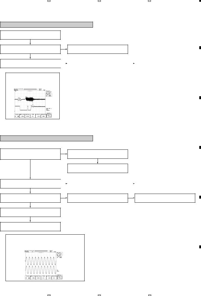
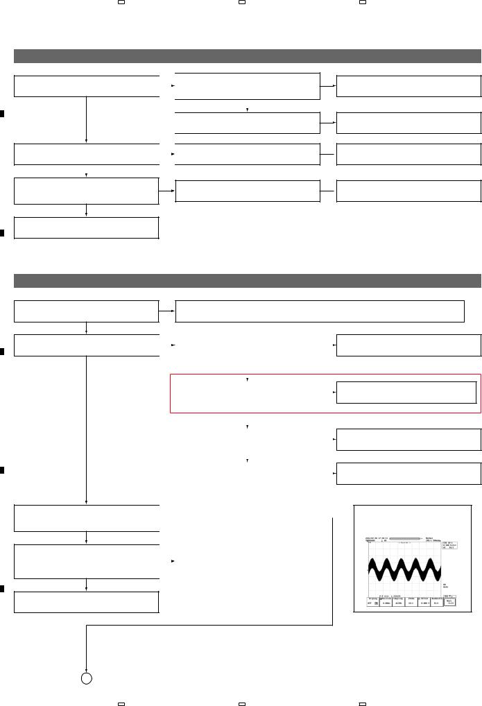
3. Spindle motor system check
Does the unit try to start playing when the OPEN/CLOSE button is pressed without a disc loaded?
No
1.Can the spindle motor turn a little? (See the waveforms in Fig. 4.)
No
2. The spindle motor cannot turn.
Yes
The circuit of the spindle-motor driver is normal.
Yes |
Check the peripheries of Pin 114 of U901 and |
|
Replace the MAIN Assy. |
||
|
|
Pins 11, 12 and 4 of U903. |
|
|
|
|
|
|
|
||
|
|
|
|
|
|
1U901 - pin 111 (FOSO) V: 0.2 V/div. H: 1 s/div.
4U901 - pin 114 (DMSO) V: 1 V/div. H: 1 s/div.
1
4
Fig. 4 Waveform
4. Miscellaneous
The RF waveform is normal and the time is displayed normally, but no sound is output or sound is interrupted.
1. Are the waveforms indicated in Fig. 5 output from Pins 65 and 66 of U901 when a 1-kHz
No Error correction is not possible because of
signal is played?
scratches or dirt on the disc.
Yes
Check if playback is possible, using a proper disc.
2.Are the waveforms indicated in Fig. 5 output from Pins 23 and 24 of IC503?
Yes
3.Are the waveforms indicated in Fig. 5 output from Pins 22 and 32 of IC504?
Yes
4. If Yes, check the periphery of IC302.
Replace the MAIN Assy.
No |
Check the periphery of IC504, U907, Q917 and |
|
Replace the MAIN Assy. |
||
|
|
Q918. |
|
|
|
|
|
|
|
||
|
|
|
|
|
|
No
Check the peripheries of IC601. (X-EM21V only) Replace the MAIN Assy.
5U901 - pin 65, IC504 - pin 24, IC302 - pin 22 (Lch) V: 1 V/div. H: 1 ms/div.
6U901 - pin 66, IC504 - pin 23, IC302 - pin 32 (Rch) V: 1 V/div. H: 1 ms/div.
5
6
Fig. 5 Waveform
X-EM21V |
13 |
A
B
C
D
E
F
|
5 |
|
6 |
|
7 |
|
8 |
|
|
|
|
|
|
|
1 |
|
2 |
|
3 |
|
4 |
|
|
|
|
|
|
A |
[2] Operations with a USB memory device not possible |
|
"NO USB" is displayed.
1.Check power from U901 (SPHE8202RQ-D) and XP906.
2.Check the communication line between IC701 (CA6817) and U901 (SPHE8202RQ-D).
[3]Data in a USB memory device cannot be played.
Data in the USB memory device cannot be played even if the USB operation key is pressed.
1. Check the DP data line. B 2. Check the DM data line.
USB system check
Select the USB function, by pressing the INPUT button on the main unit (USB button on the remote control unit), then plug a USB memory device into the USB connector.
1. Can the device information be displayed?
Yes
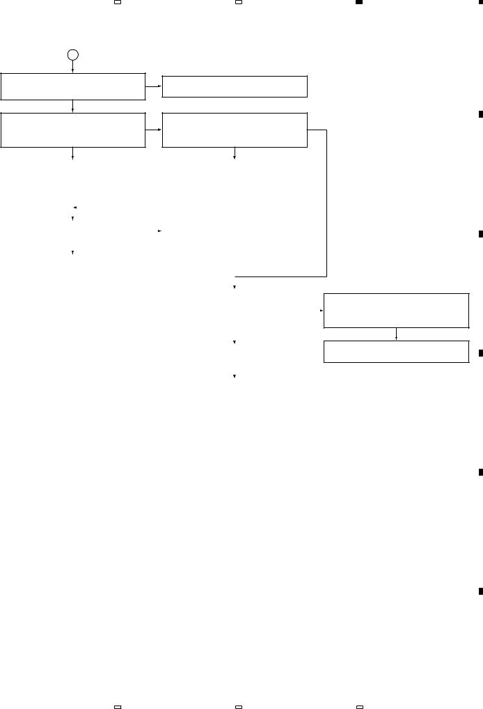
2.When a 1-kHz signal is played, are the waveforms indicated in Fig. 8 output from Pins 65 and 66 of U901?
C |
Yes |
3.Are the waveforms indicated in Fig. 8 output from Pins 23 and 24 of IC504?
Yes
4.Are the waveforms indicated in Fig. 8 output from Pins 22 and 32 of IC302?
Yes
No Check Pins 80 and 79 of U901 or check the
Replace the MAIN Assy.
peripheries of Pins 12, 13 and 5. (See Figs. 6 and 7.)
No
Check Pins 65 and 66 of U901.
No
Check the periphery of IC504.
No Check the peripheries of IC601. (X-EM21V only)
 Replace the MAIN Assy.
 Replace the MAIN Assy.
 Replace the MAIN Assy.
|
5. If Yes, check the periphery of IC302. |
|
|
|
|
|
|
|
|
|
|
D |
Replace the MAIN Assy. |
|
|
|
|
|
|
7 U901 - pin 80 (DM) |
|
9 |
U901 - pin 12 (DVD-TXD) |
|
5 U901 - pin 65, IC504 - pin 24, IC302 - pin 22 (Lch) |
|||
|
|
V: 2 V/div. |
H: 500 ns/div. |
|
|
V: 2 V/div. |
H: 500 μs/div. |
|
V: 1 V/div. |
H: 1 ms/div. |
|
|
|
|
|||||||
|
|
8 U901 - pin 79 (DP) |
|
a U901 - pin 11 (DVD_RXD) |
|
6 U901 - pin 66, IC504 - pin 23, IC302 - pin 32 (Rch) |
||||
|
|
|||||||||
|
|
V: 2 V/div. |
H: 500 ns/div. |
|
|
V: 2 V/div. |
H: 500 μs/div. |
|
V: 1 V/div. |
H: 1 ms/div. |
|
|
|
|
|
b U901 - pin 5 (URST#) |
|
|
|
||
|
|
|
|
|
|
V: 2 V/div. |
H: 500 μs/div. |
|
|
|
|
|
7 |
|
|
|
|
|
|
5 |
|
|
|
|
|
|
|
|
|
|
|
|
E |
|
|
|
|
9 |
|
|
|
|
|
8 |
|
|
|
|
|
|
6 |
|
||
|
|
|
|
|
a |
|
|
|
||
|
|
|
|
|
|
|
|
|
||
|
|
|
|
|
|
b |
|
|
|
|
|
|
|
|
|
|
|
|
|
|
|
|
Fig. 6 Waveform |
Fig. 7 Waveform |
Fig. 8 Waveform |
|
|
||||
F |
|
|
|
|
14 |
|
|
|
|
|
X-EM21V |
|
||
|
|
|
|
|
|
1 |
|
2 |
|
3 |
|
4 |
|
|
|
|
|
|
|
5 |
|
6 |
|
7 |
|
8 |
|
|
|
|
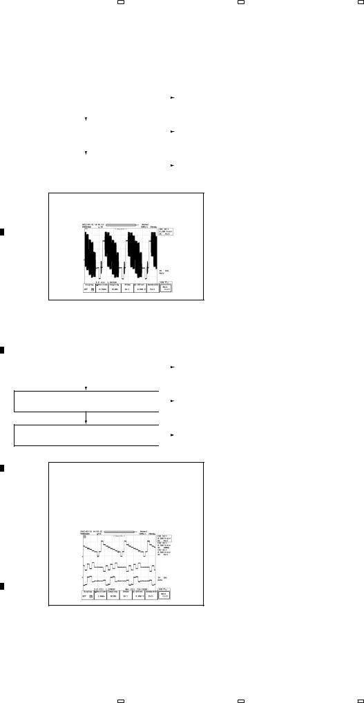
[4] Operations with an iPod are not possible (only for the X-EM21V)
The message "iPod" remains displayed on the LCD.
1.Check power from IC403 (IPOD+5V).
2.Check the iPod communication line between IC701 (CA6817) and CN601.
Check of the iPod system
Select the iPod function, by pressing the INPUT button on the main unit (iPod button on the remote control unit), then insert an iPod into the iPod dock to connect it with the DOCK connector.
1. Can the device information be displayed?
Yes
2.When a 1-kHz signal is played, are the waveforms indicated in Fig. 11 output from Pins 23 and 24 of IC504?
Yes
3.Are the waveforms indicated in Fig. 11 output from Pins 22 and 32 of IC302?
Yes
No
No
No
Check Pins 30 and 31 of IC701 or check the
Replace the MAIN Assy.
peripheries of Pins 32, 33, and 34. (See Figs. 9 and 10.)
Check the peripheries of CN601, IC602 and |
|
|
Replace the MAIN Assy. |
IC504. |
|
|
|
|
|
|
|
|
|
|
|
Check the peripheries of IC601. |
|
|
Replace the MAIN Assy. |
(X-EM21V only) |
|
|
|
|
|
|
|
|
|
|
|
4. If Yes, check the periphery of IC302.
Replace the MAIN Assy.
A
B
C
c IC701 - pin 30 |
(DET30) |
e IC701 - pin 32 |
(IPOD_CON) |
h IC504 - pin 24, IC302 - pin 22 |
(Lch) |
|
|||
V: 2 V/div. |
H: 10 ms/div. |
V: 2 V/div. |
H: 2 ms/div. |
V: 1 V/div. |
H: 1 ms/div. |
|
|
||
|
|
||||||||
d IC701 - pin 31 |
(DPET13) |
f IC701 - pin 33 |
(IP_TX) |
i IC504 - pin 23, IC302 - pin 32 |
(Rch) |
|
|||
V: 2 V/div. |
H: 10 ms/div. |
V: 2 V/div. |
H: 2 ms/div. |
V: 1 V/div. |
H: 1 ms/div. |
|
|
||
gIC701 - pin 34 (IP_RX) V: 2 V/div. H: 2 ms/div.
c |
|
|
|
h |
||
|
|
|
|
|||
d |
|
e |
|
D |
||
|
|
i |
||||
|
|
|
|
|||
|
|
f |
|
|
|
|
|
|
g |
|
|
|
|
|
|
|
|
|
|
|
Fig. 9 Waveform |
|
Fig. 10 Waveform |
Fig. 11 Waveform |
|
||
|
||||||
E
F
X-EM21V |
15 |
|
5 |
|
6 |
|
7 |
|
8 |
|
|
|
|
|
|
|
1 |
|
2 |
|
3 |
|
4 |
|
|
|
|
|
|
A |
[5] No power |
|
Is the Power indictor lit?
Yes
Does the voltage at Pin 11 of CN801 (AD1) become 0.4 V when the uSTANDBY/ON button is pressed?
B |
Yes |
|
Does the voltage at Pin 4 of IC701 (AD1) on the MAIN board become 0.4 V when the
uSTANDBY/ON button is pressed?
Yes
IC701 is defective. Replace the MAIN Assy.
|
No |
|
Check if the voltage at Pins 1 and 2 of CN1102 |
||
|
|
||||
|
|
on the SMPS Assy and of CN402 on the MAIN |
|||
|
|
|
|
||
|
|
|
|
Assy is 13 V. |
|
|
|
|
|
|
OK |
|
|
|
|
|
|
|
|
|
|
Check that the voltage from IC402 is 3.3 V. |
|
|
|
|
|
||
|
No |
|
The FFC, CN701, or SW701 is defective. |
||
|
|
||||
|
|
||||
|
|
|
|
||
|
|
|
|
|
|
No
CN703 is defective.
NG The SMPS Assy or the connection cable may be defective and require replacement.
NG
IC310 is defective. Replace the MAIN Assy.
NG
 Replace the FFC or the DISPLAY LCD Assy.
NG
 Replace the MAIN Assy.
[6] No sound
C
Is sound from any source not output?
Yes
No To the flowchart "Operations with a CD (USB memory device, iPod) not possible," depending on which audio source's sound is not output
Is sound output from the headphones?
Yes
D
Check the output from Pins 2, 3, 8, and 9 (for Ch. R) and 10, 11, 16, and 17 (for Ch. L) of TDA7491HV
(IC302) of the POWER amplifier. (Fig. 12)
E
OK
Check the signals output from Pins 2, 3, 8, and 9 (for Ch. R) and 10, 11, 16, and 17 (for Ch. L) of TDA7491HV (IC302) of the POWER amplifier to the SP terminals.
OK
|
No |
Check the output from Pins 23 and 24 of |
NG |
|||
|
|
|
SC7314 (IC504) of the SIGNAL SELECT switch. |
|
|
|
|
|
|
|
|
|
|
|
|
|
|
OK |
|
|
|
X-EM21V only |
|
|
|
||
|
|
|
|
|
NG |
|
|
|
|
|
|||
|
|
|
Check the output from Pins 2 and 7 of M62429 |
|||
|
|
|
(IC601) of the VOL control. |
|
|
|
|
|
|
|
|
|
|
|
|
|
|
OK |
|
|
|
|
|
|
|
NG |
|
|
|
|
|
|||
|
|
|
Check the output from Pins 1 and 7 of ETK4800 |
|||
|
|
|
(IC501) of the OP amplifier. |
|
|
|
|
|
|
|
|
|
|
|
|
|
|
OK |
|
|
|
|
|
|
|
NG |
|
|
|
|
Check the output from Pins 6 and 7 of CN506 |
|||
|
NG |
on the AUX Assy. |
|
|
||
|
|
|
|
|
||
|
|
|
|
|
||
|
|
|
|
|
||
|
NG |
|
|
|
|
|
|
|
|
|
|||
|
|
|
|
|
||
|
Something on the corresponding line is in failure. |
|
|
|||
|
|
|
Replace the MAIN Assy. |
|
|
|
|
|
|
|
|
|
|
|
|
|
|
|
|
|
The SP terminals are defective. Replace the MAIN Assy.
F
Play a CD and check the output from Pins 8 and 13 of SC7314 (IC504) of the SIGNAL SELECT switch.
M62429 (IC601) of the VOL control is defective. Replace the MAIN Assy.
ETK4800 (IC501) of the OP amplifier is defective. Replace the MAIN Assy.
The AUX Assy is defective.
Replace the AUX Assy.
IC302 - pin 2, 3, 8, 9 (Rch)
V: 0.5 V/div. H: 500 μs/div. <Input signal: 1kHz-0dB, Vol : 10>
Fig. 12 Waveform
A
16 |
X-EM21V |
|
1 |
|
2 |
|
3 |
|
4 |
|
|
|
|
|
|
|
5 |
|
6 |
|
7 |
|
|
|
A
NG
Has the protection circuit for TDA7491HV (IC302) of the POWER amplifier been activated (is the signal level from Pin 28 high)?
Yes
Has overvoltage protection been activated for TDA7491HV (IC302) of the POWER amplifier ? (Is the voltage at Pins 6, 7, 12, and 13 20 V or higher?)
Yes
No
No
TDA7491HV (IC302) of the POWER amplifier is defective. Replace the MAIN Assy.
Has undervoltage protection been activated for TDA7491HV (IC302) of the POWER amplifier? No (Is the voltage at Pins 6, 7, 12, and 13 4 V or
lower?)
Yes
Failure in power supply (Because of an error in |
|
|
Failure in power supply (Because of an error in |
|
||||
SMPS Assy, the supply voltage, which should be |
|
|
SMPS Assy or damage on L6, the supply voltage, |
|
||||
+13 V, becomes 20 V or higher.) In effect, |
|
|
which should be +13 V, becomes 4V or lower.) |
|
||||
there is possibility that other ICs are damaged. |
|
|
|
|
|
|||
|
|
|
||||||
|
|
|
|
|
|
|
|
|
|
|
|
|
|
|
|
|
|
|
|
|
NG |
|
|
|
|
|
|
|
|
|
|
|
|
||
Check if the voltage at Pins 1 and 2 of CN1102 on the |
|
The SMPS Assy or the connection cable may be |
|
|||||
SMPS Assy and of CN402 on the MAIN Assy is 13 V. |
|
|
|
defective and require replacement. |
|
|||
|
|
|
|
|
|
|
|
|
|
OK |
|
|
|
||||
|
|
|
|
|
|
|
|
|
Replace the MAIN Assy. |
|
|
|
|
|
|
||
|
|
|
|
|
|
|
|
|
|
|
|
|
|
|
|
|
|
|
|
|
|
|
|
|
|
|
|
|
|
|
|
|
Has overcurrent protection been activated for |
|
|
|
|
|
|
|
|
TDA7491HV (IC302) of the POWER amplifier? |
No |
|
|
|
|
|
|
|
(Is the voltage at Pins 2, 3, 8, and 9 [for Ch. R] |
||
|
|
|
|
|
|
|
||
|
|
|
|
|
|
or 10, 11, 16, and 17 [for Ch. L] 0 V |
|
|
|
|
|
|
|
|
[short-circuited]?) |
|
|
|
|
|
|
|
|
|
|
|
|
|
|
|
|
|
|
Yes |
|
|
|
|
|
|
|
|
|
|
|
|
|
|
|
|
Check the periphery of the speaker terminals. |
|
|
|
|
|
|
|
|
|
|
|
|
|
|
|
|
|
|
OK |
|
|
|
|
|
|
|
|
|
|
|
|
|
|
|
|
Replace the MAIN Assy. |
|
|
|
|
|
|
|
|
|
|
|
8
A
B
C
Has thermal protection been activated for TDA7491HV (IC302) of the POWER amplifier? Can the unit restart after this IC is cooled down using a point cooler?
Yes
IC302 is defective. Replace the MAIN Assy.
D
E
F
X-EM21V |
17 |
|
5 |
|
6 |
|
7 |
|
8 |
|
|
|
|
|
|
|
1 |
|
2 |
|
3 |
|
4 |
|
|
|
|
|
|
A |
[7] No picture (DVD) |
|
|
||||
|
|
|
|
||||
|
|
[COMPOSITE] |
|
|
|||
|
|
|
|
No |
|
|
|
|
|
Is sound output? |
To the flowchart "Operations with a DVD or CD |
|
|||
|
|
|
|
not possible". |
|
||
|
|
|
|
|
|
|
|
|
|
|
|
|
|
|
|
|
|
|
Yes |
|
|
||
|
|
|
|
No |
|
|
|
|
|
Check the output from Pin 69 of U901. (Fig. 13) |
U901 (SPHE8202RQ) is defective. |
|
|||
|
|
|
|
Replace the MAIN Assy. |
|
||
|
|
|
|
|
|
|
|
|
|
|
|
|
|
|
|
|
|
|
Yes |
|
|
||
|
|
|
|
|
|||
|
|
Check the output from XP905 (VIDEO). (Fig. 13) |
No |
L909 or D910 or XP905 (VIDEO) is defective. |
|
||
B |
|
|
Replace the MAIN Assy. |
|
|||
|
|
|
|
|
|||
|
|
|
|
|
|
||
iU901 - pin 69 (V_CVBS), XP905 (VIDEO) V: 0.2 V/div. H: 20 μs/div.
<Input signal: COLOR BAR>
i
C
Fig. 13 Waveform
[COMPONENT]
Is sound output? |
No |
To the flowchart "Operations with a DVD or CD |
||
|
|
not possible". |
||
|
|
|
|
|
|
|
|
|
|
|
Yes |
|
||
Check the output from Pins 73 (Y), 74 (Pb/Cb),
75 (PR/Cr) of U901. (Fig. 14)
D
Yes
Check the output from XP905 (Y, Pb/Cb, Pr/Cr). (Fig. 14)
No |
U901 (SPHE8202RQ) is defective. |
||
|
|
Replace the MAIN Assy. |
|
|
|
|
|
|
|
|
|
No |
L907 or D908 or XP905 (Y), L908 or D909 or |
||
XP905 (Pb/Cb), L906 or D907 or XP905 (Pr/Cr) |
|||
|
|
||
|
|
is defective. Replace the MAIN Assy. |
|
|
|
|
|
j U901 - pin 73 (V_G/Y), XP905 (Y) V: 0.5 V/div. H: 20 μs/div.
kU901 - pin 74 (V_B/U), XP905 (Pb/Cb) V: 0.5 V/div. H: 20 μs/div.
lU901 - pin 75 (V_R/V), XP905 (Pr/Cr) V: 0.5 V/div. H: 20 μs/div.
<Input signal: COLOR BAR>
E
j
k
l
Fig. 14 Waveform
F
18 |
X-EM21V |
|
1 |
|
2 |
|
3 |
|
4 |
|
|
|
|
|
|
 Loading...