

Page 1
BDP-LX54
For details, refer to "Important Check Points for good servicing".
Blu-ray 3D™ PLAYER
BDP-LX54
BDP-43FD
BDP-430
BDP-41FD
THIS MANUAL IS APPLICABLE TO THE FOLLOWING MODEL(S) AND TYPE(S).
ORDER NO .
RRV4152
Model Type Power Requirement
BDP-LX54 YXV5 AC 220 V to 240 V B 2
BDP-LX54 SXV AC 220 V to 240 V C 5
BDP-43FD UCXV AC 120 V A 1
BDP-430 UCXVSM AC 120 V A 1
BDP-430 YXV5 AC 220 V to 240 V B 2
BDP-430 SXV AC 220 V to 240 V C 5
BDP-41FD UCXV AC 120 V A 1
PIONEER CORPORATION 1-1, Shin-ogura, Saiwai-ku, Kawasaki-shi, Kanagawa 212-0031, Japan
PIONEER ELECTRONICS (USA) INC. P.O. Box 1760, Long Beach, CA 90801-1760, U.S.A.
PIONEER EUROPE NV Haven 1087, Keetberglaan 1, 9120 Melsele, Belgium
PIONEER ELECTRONICS ASIACENTRE PTE. LTD. 253 Alexandra Road, #04-01, Singapore 159936
BD
Region No.
DVD
Region No.
Remarks
K-IZA OCT.
2010 Printed in Japan
Page 2
1
WARNING
This product may contain a chemical known to the State of California to cause cancer, or birth defects or other reproductive
harm.
Health & Safety Code Section 25249.6 - Proposition 65
This service manual is intended for qualified service technicians; it is not meant for the casual do-ityourselfer. Qualified technicians have the necessary test equipment and tools, and have been trained
to properly and safely repair complex products such as those covered by this manual.
Improperly performed repairs can adversely affect the safety and reliability of the product and may
void the warranty. If you are not qualified to perform the repair of this product properly and safely, you
should not risk trying to do so and refer the repair to a qualified service technician.
1. SAFETY PRECAUTIONS
The following check should be performed for the
continued protection of the customer and service
technician.
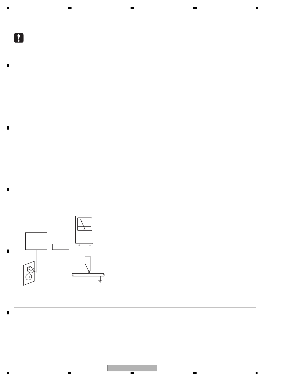
LEAKAGE CURRENT CHECK
Measure leakage current to a known earth ground
(water pipe, conduit, etc.) by connecting a leakage
current tester such as Simpson Model 229-2 or
equivalent between the earth ground and all exposed
metal parts of the appliance (input/output terminals,
screwheads, metal overlays, control shaft, etc.). Plug
the AC line cord of the appliance directly into a 120 V
AC 60 Hz outlet and turn the AC power switch on. Any
current measured must not exceed 0.5 mA.
ANY MEASUREMENTS NOT WITHIN THE LIMITS
OUTLINED ABOVE ARE INDICATIVE OF A POTENTIAL
SHOCK HAZARD AND MUST BE CORRECTED BEFORE
RETURNING THE APPLIANCE TO THE CUSTOMER.
2. PRODUCT SAFETY NOTICE
Many electrical and mechanical parts in the appliance
have special safety related characteristics. These are
often not evident from visual inspection nor the protection
afforded by them necessarily can be obtained by using
replacement components rated for voltage, wattage, etc.
Replacement parts which have these special safety
characteristics are identified in this Service Manual.
Electrical components having such features are
identified by marking with a > on the schematics and on
the parts list in this Service Manual.
The use of a substitute replacement component which
does not have the same safety characteristics as the
PIONEER recommended replacement one, shown in the
parts list in this Service Manual, may create shock, fire,
or other hazards.
Product Safety is continuously under review and new
instructions are issued from time to time. For the latest
information, always consult the current PIONEER Service
Manual. A subscription to, or additional copies of,
PIONEER Service Manual may be obtained at a nominal
charge from PIONEER.
Leakage
current
tester
Reading should
not be above
0.5 mA
Device
under
test
Test all
exposed metal
surfaces
Also test with
plug reversed
(Using AC adapter
plug as required)
Earth
ground
AC Leakage Test
(FOR USA MODEL ONLY)
2 3 4
SAFETY INFORMATION
A
B
C
D
E
F
2
1
2 3 4
BDP-LX54
Page 3
5
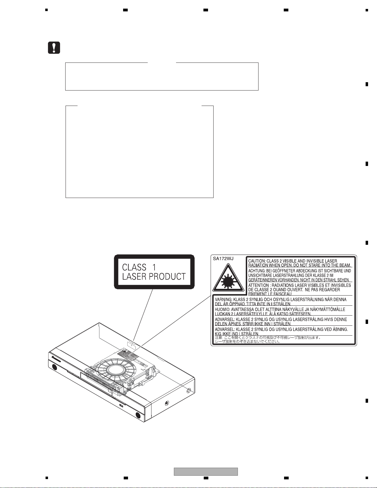
LABEL CHECK
The following caution label appears on your unit.
Location: inside of the unit
WARNING !
THE LASER COMPONENT IS CAPABLE OF EMITTING RADIATION EXCEEDING THE LIMIT
FOR CLASS 1.
A SPECIALLY INSTRUCTED PERSON SHOULD DO SERVICING OPERATION OF THE
APPARATUS.
Laser Pickup specifications and Laser characteristics
For BD Wave length : 405 nm
Operating output :
SL : 0.32
DL : 0.64 mW CW, Class 1
Maximum output : Class 2 (under fault condition)
For DVD Wave length : 660 nm
Operating output : 0.40 mW CW, Class 1
Maximum output : Class 1 (under fault condition)
For CD Wave length : 785 nm
Operating output : 0.41 mW CW, Class 1
Maximum output : Class 1 (under fault condition)
(Printed on the Rear Panel)
6 7 8
A
B
C
D
E
F
BDP-LX54
5
6 7 8
3
Page 4
1
[Important Check Points for Good Servicing]
In this manual, procedures that must be performed during repairs are marked with the below symbol.
Please be sure to confirm and follow these procedures.
1. Product saf ety
Please conform to product regulations (such as safety and radiation regulations), and maintain a safe servicing environment b y
following the safety instructions described in this manual.
1 Use specified parts for repair.
Use genuine parts. Be sure to use important parts for safety .
2 Do not perform modifications without proper instructions.
Please follow the specified safety methods when modification(addition/change of parts) is required due to interferences such as
radio/TV interf erence and foreign noise .
3 Make sure the soldering of repaired locations is properly performed.
When you solder while repairing, please be sure that there are no cold solder and other debris.
Soldering should be finished with the proper quantity . (Refer to the e xample)
4 Make sure the screws are tightly fastened.
Please be sure that all screws are fastened, and that there are no loose screws .
5 Make sure each connectors are correctly inserted.
Please be sure that all connectors are inserted, and that there are no imperfect insertion.
6 Make sure the wiring cables are set to their original state.
Please replace the wiring and cables to the original state after repairs.
In addition, be sure that there are no pinched wires, etc.
7 Make sure screws and soldering scraps do not remain inside the product.
Please check that neither solder debris nor screws remain inside the product.
8 There should be no semi-broken wires , scratches, melting, etc. on the coating of the pow er cord.
Damaged power cords may lead to fire accidents, so please be sure that there are no damages .
If you find a damaged power cord, please exchange it with a suitab le one.
9 There should be no spark traces or similar marks on the power plug.
When spark traces or similar marks are found on the power supply plug, please check the connection and advise on secure
connections and suitable usage. Please exchange the po wer cord if necessary .
a Safe en vironment should be secured during servicing.
When you perform repairs, please pay attention to static electricity, furniture, household articles, etc. in order to prev ent injuries.
Please pay attention to your surroundings and repair safely.
2. Adjustments
T o k eep the original performance of the products, optimum adjustments and confirmation of characteristics within specification.
Adjustments should be performed in accordance with the procedures/instructions described in this manual.
4. Cleaning
For parts that require cleaning, such as optical pickups, tape deck heads, lenses and mirrors used in projection monitors, proper
cleaning should be performed to restore their performances.
3. Lubricants, Glues , and Replacement parts
Use grease and adhesives that are equal to the specified substance.
Make sure the proper amount is applied.
5. Shipping mode and Shipping scre ws
T o protect products from damages or f ailures during transit, the shipping mode should be set or the shipping screws should be
installed before shipment. Please be sure to follo w this method especially if it is specified in this manual.
A
2 3 4
B
C
D
E
F
4
1
BDP-LX54
2 3 4
Page 5

5
6 7 8
CONTENTS
SAFETY INFORMATION..........................................................................................................................................................2
1. SERVICE PRECAUTIONS....................................................................................................................................................6
1.1 NOTES ON SOLDERING............................................................ .......................................... .........................................6
1.2 IMPOTANT SERVICE NOTICE.......................................................................................................................................6
2. SPECIFICATIONS.................................................................................................................................................................7
2.1 SPECIFICATIONS ..........................................................................................................................................................7
2.2 DISC/CONTENT FORMAT.............................. .......................................... .....................................................................8
2.3 PANEL FACILITIES........................................................ .......................................... .....................................................13
3. BASIC ITEMS FOR SERVICE............................................................................................................................................15
3.1 CHECK POINTS AFTER SERVICING .................................................................... .....................................................15
3.2 PCB LOCATIONS.................................... .......................................... ...........................................................................16
3.3 JIGS LIST............................... ... .......................................... .........................................................................................17
4. BLOCK DIAGRAM..............................................................................................................................................................18
4.1 OVERALL WIRING DIAGRAM.....................................................................................................................................18
4.2 OVERALL BLOCK DIAGRAM............................. .......................................... ................................................................20
4.3 POWER SUPPLY BLOCK DIAGRAM...........................................................................................................................22
5. DIAGNOSIS........................................................................................................................................................................24
5.1 DIAGNOSIS FLOWCHART..........................................................................................................................................24
5.2 TROUBLESHOOTING....................................................................... ...........................................................................25
6. SERVICE MODE.................................................................................................................................................................29
6.1 INFORMATION SCREEN DISPLAY AND THE FACTORY DEFAULT SETTINGS.......................................................29
6.2 MEASUREMENT OF ERROR RATES .........................................................................................................................30
7. DISASSEMBLY ...................................................................................................................................................................32
8. EACH SETTING AND ADJUSTMENT................................................................................................................................38
8.1 NECESSARY ITEMS TO BE NOTED...........................................................................................................................38
8.2 UPDATING OF THE FIRMWARE.................................................................................................................................38
9. EXPLODED VIEWS AND PARTS LIST...............................................................................................................................40
1 PACKING SECTION................................ .. .......................................... .........................................................................40
9.
9.2 EXTERIOR SECTION ..................................................................................................................................................42
9.3 FRONT PANEL SECTION............................................................................................................................................44
10. SCHEMATIC DIAGRAM............................................... ... ... ................................................ .. .............................................46
10.1 MAIN PWB-S (1/6)................................... ... .......................................... ......................................................................46
10.2 MAIN PWB-S (2/6)................................... ... .......................................... ......................................................................48
10.3 MAIN PWB-S (3/6)................................... ... .......................................... ......................................................................50
10.4 MAIN PWB-S (4/6)................................... ... .......................................... ......................................................................52
10.5 MAIN PWS-S (5/6)................................... ... .......................................... ......................................................................54
10.6 MAIN PWB-S (6/6)................................... ... .......................................... ......................................................................56
10.7 FLKB PWB-S..............................................................................................................................................................58
10.8 MTFB and USBB ASSYS...........................................................................................................................................60
10.9 LEDB ASSY................................................................................................................................................................61
10.10 KEYB and 232C ASSYS...........................................................................................................................................62
10.11 POWER ASSY (POWER PWB-S)............................................................................................................................64
10.12 BRIDGE ASSY .........................................................................................................................................................66
11. PCB CONNECTION DIAGRAM............................................ ... ............................................... ... ... ....................................68
11.1 MAIN PWB-S..............................................................................................................................................................68
11.2 FLKB PWB-S..............................................................................................................................................................76
11.3 MTFB and USBB ASSYS...........................................................................................................................................78
11.4 LEDB
, KEYB
11.5 POWER ASSY (POWER PWB-S)..............................................................................................................................82
12. PCB PARTS LIST...................................... ... .......................................... ...........................................................................84
and 232C ASSYS.................................................................................................................................80
A
B
C
D
E
F
BDP-LX54
5
6 7 8
5
Page 6

1
• For environmental protection, lead-free solder is used on the printed circuit boards mounted in this unit.
Be sure to use lead-free solder and a soldering iron that can meet specifications for use with lead-free solders for repairs
accompanied by reworking of soldering.
• Compared with conventional eutectic solders, lead-free solders have higher melting points, by approximately 40 ºC.
Therefore, for lead-free soldering, the tip temperature of a soldering iron must be set to around 373 ºC in general, although
the temperature depends on the heat capacity of the PC board on which reworking is required and the weight of the tip of
the soldering iron.
Do NOT use a soldering iron whose tip temperature cannot be controlled.
Compared with eutectic solders, lead-free solders have higher bond strengths but slower wetting times and higher melting
temperatures (hard to melt/easy to harden).
The following lead-free solders are available as service parts:
• Parts numbers of lead-free solder:
GYP1006 1.0 in dia.
GYP1007 0.6 in dia.
GYP1008 0.3 in dia.
1. The MAIN PWB-S needs to be replaced as a whole unit.
2. If the MAIN PWB-S is replaced, perform the section "8.2 UPDATING O F T H E FIRMWARE" and confirm the version:
it is necessary to update to the latest version if the MAIN PWB-S version is old.
2 3 4
1. SERVICE PRECAUTIONS
1.1 NOTES ON SOLDERING
A
B
C
D
1.2 IMPOTANT SERVICE NOTICE
E
F
6
1
2 3 4
BDP-LX54
Page 7
5
General
Power requirements AC 220 V to 240 V, 50 Hz/60 Hz (European and Russian models)
AC 120 V/60 Hz (North America model)
Power consumption (Normal) 23 W
Power consumption (Standby) 0.6 W
Dimensions BDP-LX54 and BDP-43FD: 420 mm × 72.5 mm × 228 mm (W × H × D)
BDP-430 and BDP-41FD: 420 mm × 68 mm × 228 mm (W × H × D)
Weight BDP-LX54 and BDP-43FD: 3.3 kg
BDP-430 and BDP-41FD: 2.5 kg
Operating temperature 5 °C to 35 °C
Storage temperature –20 °C to 55 °C
Operating humidity 10 % to 80 % (no condensation)
TV systems NTSC system (North America model)
PAL system/NTSC system (Other models)
Playback
Playable discs BD-ROM, BD-RE Dual Layer, BD-R Dual Layer,
DVD Video, DVD-RW/-R/+RW/+R Dual Layer (Video/VR/AVCHD format),
Audio CD (CD-DA), CD-RW/-R (CD-DA, MP3, JPEG file format)
Region code European model: B or All Region for BD, 2 or ALL for DVD
Russian model: C or All Region for BD, 5 or ALL for DVD
North America model: A or All Region for BD, 1 or ALL for DVD
Input/Output
HDMI OUT HDMI 19-pin standard connector (5 V, 250 mA)
COMPONENT VIDEO OUTPUT Output level:
Y: 1 Vp-p (75 ohms)
P
B, PR: 0.7 Vp-p (75 ohms)
Jacks: RCA jack
VIDEO OUTPUT Output level: 1 Vp-p (75 ohms)
Jack: RCA jack
DIGITAL OUT OPTICAL Terminal: Square Optical terminal
AUDIO OUTPUT Output level: 2 V rms (Output impedance: 1 k ohms)
Jacks: RCA jack
USB Two sets (1 front, 1 rear), USB 2.0 High Speed (480 Mbit/s) correspondence
LAN (10/100) 10BASE-T/100BASE-TX
The specifications and design of this product are subject to change without notice.
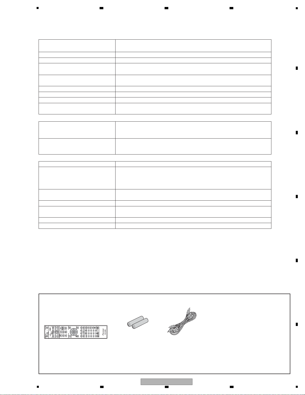
• Accessories
• Remote control unit
(BDP-LX54/YXV5, SXV: VXX3385)
(BDP-43FD/UCXV: VXX3386)
(BDP-430/UCXVSM, BDP-41FD/UCXV: VXX3383)
(BDP-430/YXV5, SXV: VXX3382)
• Dry cell battery
(R03, AAA)
• Video/audio cable
(VDE1077)
• AC cord
(BDP-LX54/YXV5, SXV: ADG7062)
(BDP-43FD/UCXV: ADG7061)
(BDP-430/UCXVSM, BDP-41FD/UCXV: ADG7022)
(BDP-430/YXV5, SXV: ADG1154)
• Warranty card
• Operating instructions
(BDP-LX54/YXV5, SXV, BDP-430/YXV5, SXV: VRB1529)
(BDP-LX54/YXV5, BDP-430/YXV5: VRE1123)
(BDP-LX54/SXV, BDP-430/SXV: VRC1577)
(BDP-43FD/UCXV, BDP-41FD/UCXV: VRD1241)
(BDP-430/UCXVSM: VRD1242)
6 7 8
2. SPECIFICATIONS
2.1 SPECIFICATIONS
A
B
C
D
E
BDP-LX54
5
6 7 8
F
7
Page 8
1
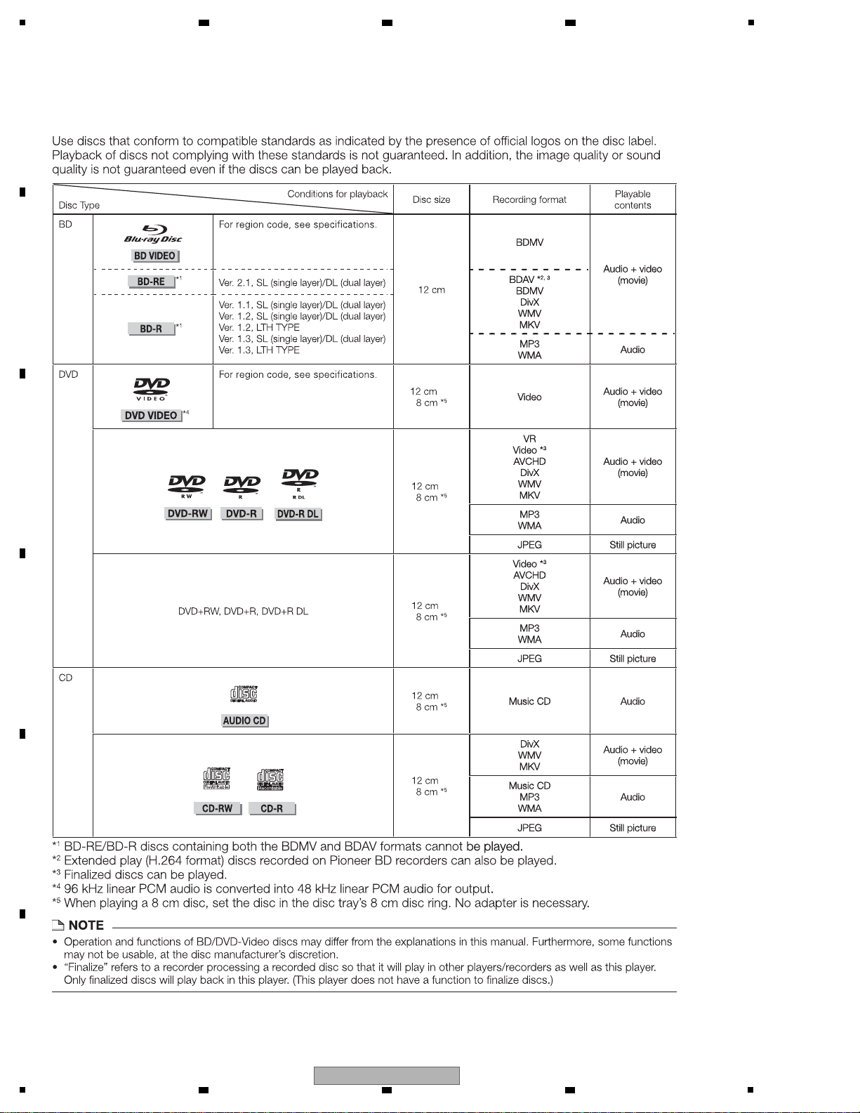
[1] Types of Discs that Can Be Used with This Player
2 3 4
2.2 DISC/CONTENT FORMAT
A
B
C
D
E
F
8
1
2 3 4
BDP-LX54
Page 9
5
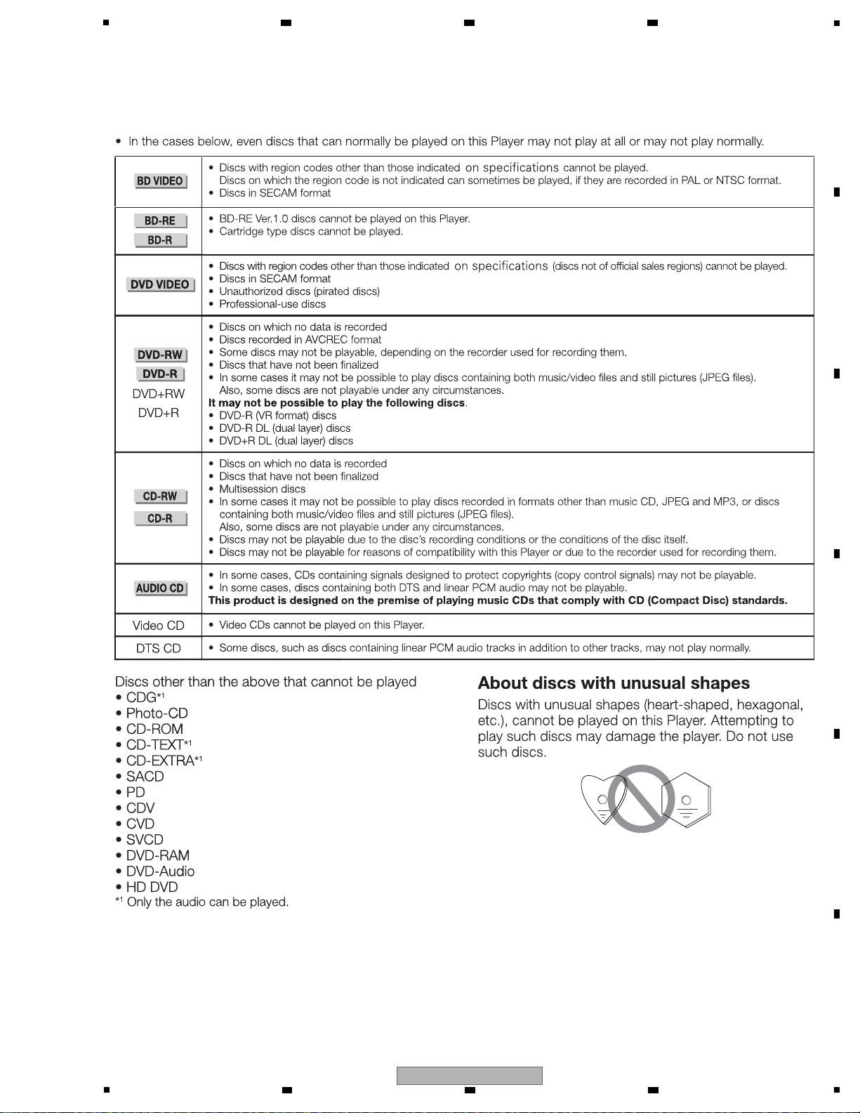
[2] Discs that Cannot Be Used with This Player
6 7 8
A
B
C
D
E
F
BDP-LX54
5
6 7 8
9
Page 10
A
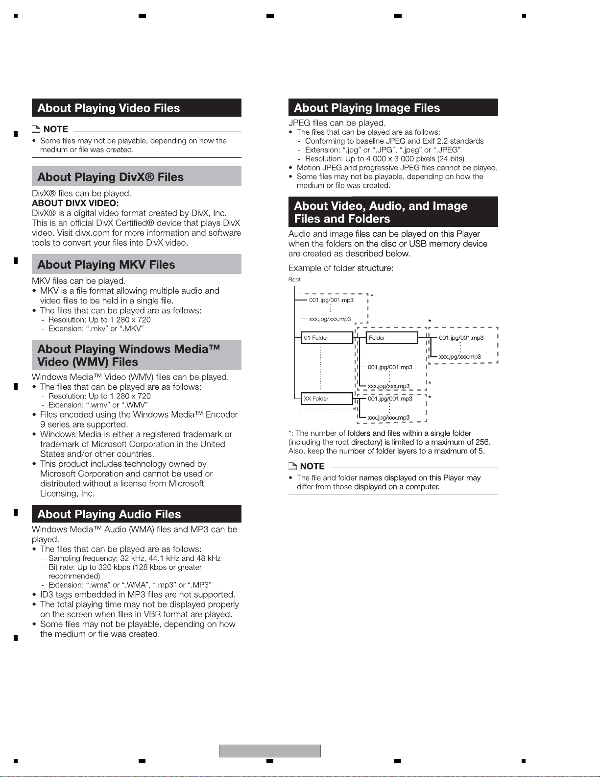
[3] About Files
B
1
2 3 4
C
D
E
F
10
1
2 3 4
BDP-LX54
Page 11
[4] About Discs
5
6 7 8
A
B
C
D
E
F
BDP-LX54
5
6 7 8
11
Page 12

1
A
B
2 3 4
C
D
E
F
12
1
2 3 4
BDP-LX54
Page 13
2.3 PANEL FACILITIES
[1] Main Unit (Front)
[2] Front Panel Display
[3] Main Unit (Rear)
(BDP-LX54, BDP-43FD, BDP-41FD only)
5
6 7 8
A
B
C
D
E
5
BDP-LX54
6 7 8
F
13
Page 14
1
[4] Remote Control Unit
A
B
2 3 4
C
D
E
F
14
1
2 3 4
BDP-LX54
Page 15
5
Specific Items to be Checked
To keep the product quality after servicing, confirm recommended check points shown below.
No.
1*
Procedures Check points
Confirm the firmware version. The version of the firmware must be latest.
Update firmware to the latest one, if it is not the latest.
2 Confirm whether the customer complain has been solved.
If the customer complain occurs with the specific disc, use it for
the operation check.
The customer complain must not be reappeared.
Video, audio and operations must be normal.
No.
1
Procedures Check points
Check that the fan motor is activated when the unit is turned on
and deactivated when the unit is turned off.
Operations must be normal.
Refer to "g Descriptions of Results" in "6.2 MEASUREMENT
OF ERROR RATES".
2 Confirm playback error rates by using the following disc.
BD-ROM test disc (GGV1308)
DVD test disc (GGV1025)
3 Play back a CD.
(track search)
Audio and operations must be normal.
4 Play back a DVD.
(Menu operation, Title/chapter search)
Video, audio and operations must be normal.
5 Play back a BD.
(Menu operation, Title/chapter search)
Video, audio and operations must be normal.
6 Check the appearance of the product.
No scratches or dirt on its appearance after receiving it for service.
See the table below for the items to be checked regarding video and audio.
Item to be checked regarding video Item to be checked regarding audio
Block noise Distortion
Horizontal noise Noise
Dot noise Volume too low
Disturbed image (video jumpiness) Volume too high
Too dark Volume fluctuating
Too bright Sound interrupted
Color disappearance
Mottled color
* Be sure to update the firmware after the MAIN PWB-S is replaced. (Refer to "8.2 UPDATING OF THE FIRMWARE".)
Items to be checked after servicing
6 7 8
3. BASIC ITEMS FOR SERVICE
3.1 CHECK POINTS AFTER SERVICING
A
B
C
D
5
6 7 8
BDP-LX54
E
F
15
Page 16
1
H
POWER ASSY
or
POWER PWB-S
A
MAIN PWB-S
G
232C ASSY
BDP-LX54, BDP-43FD,
BDP-41FD
ONLY
C
MTFB ASSY
BD DRIVE BD6P S
D
USBB ASSY
E
LEDB ASSY
B
FLKB PWB-S
F
KEYB ASSY
LIST OF ASSEMBLIES
NOTES: - Parts marked by “NSP” are generally unavailable because they are not in our Master Spare Parts List.
-
The > mark found on some component parts indicates the importance of the safety factor of the part.
Therefore, when replacing, be sure to use parts of identical designation.
Mark
Symbol and Description
BDP-LX54
/YXV5
BDP-LX54
/SXV
BDP-43FD
/UCXV
BDP-430
/UCXVSM
BDP-430
/YXV5
BDP-430
/SXV
BDP-41FD
/UCXV
MAIN PWB-S OXX9018 OXX9034 OXX9017 OXX9014 OXX9015 OXX9031 OXX9014
FLKB PWB-S OXX9019 OXX9019 OXX9019 OXX9019 OXX9019 OXX9019 OXX9019
MTFB ASSY OWZ9014 OWZ9014 OWZ9014 OWZ9013 OWZ9013 OWZ9013 OWZ9013
USBB ASSY OWZ9017 OWZ9017 OWZ9017 OWZ9016 OWZ9016 OWZ9016 OWZ9016
LEDB ASSY OWZ9020 OWZ9020 OWZ9020 OWZ9019 OWZ9019 OWZ9019 OWZ9019
KEYB ASSY OWZ9023 OWZ9023 OWZ9023 OWZ9022 OWZ9022 OWZ9022 OWZ9022
POWER PWB-S Not used Not used Not used OXX9026 OXX9027 OXX9027 Not used
232C ASSY OWZ9027 OWZ9027 OWZ9027 Not used Not used Not used OWZ9027
POWER ASSY OWZ9028 OWZ9028 OWZ9025 Not used Not used Not used OWZ9026
BD DRIVE BD6P S OXX8037 OXX8037 OXX8037 OXX8037 OXX8037 OXX8037 OXX8037
3.2 PCB LOCATIONS
A
2 3 4
B
C
D
E
F
16
1
2 3 4
BDP-LX54
Page 17
5
Jigs List
Cleaning
Name Part No. Remarks
Cleaning liquid GEM1004
Position to be cleaned
Pickup lenses
Cleaning paper GED-008
Cleaning paper GED-008
Refer to "7. DISASSEMBLY".
Refer to "9.2 EXTERIOR SECTION".FANs
Before shipping out the product, be sure to clean the following positions by using the prescribed cleaning tools.
Jig Name Part No. Remarks
Remote control unit for service GGF1067 Service mode
DVD test disc (DVD-Video) GGV1025 Check of DVD-Video
BD-ROM test disc GGV1308 Check of BD-ROM
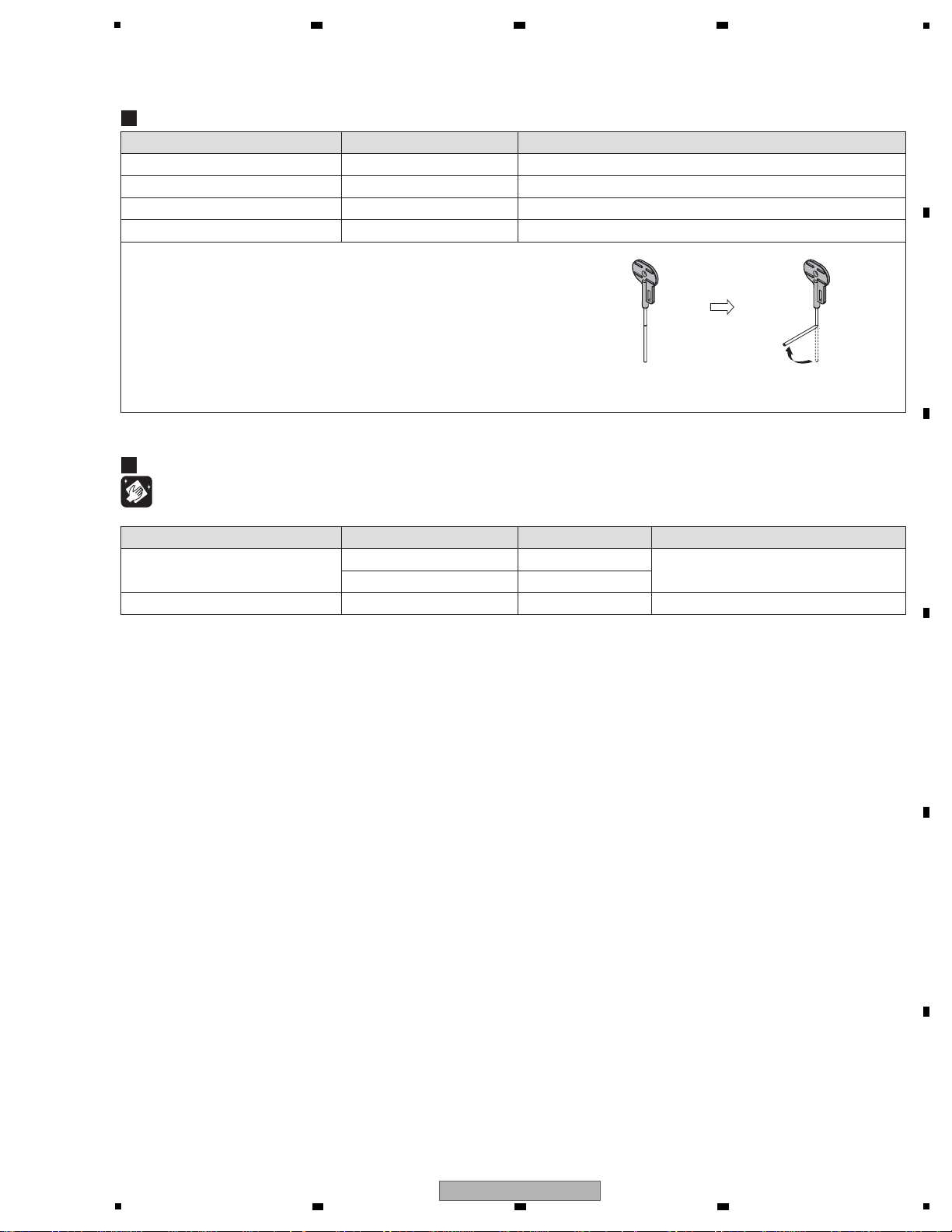
Emergency disc ejection rod
• Bend the emergency disc ejection rod already constructed
using pliers or other tools as shown in the right figure for use.
GGF1529 Emergency disc ejection
6 7 8
3.3 JIGS LIST
A
B
C
D
E
F
BDP-LX54
5
6 7 8
17
Page 18
1
FAN VDD
GND
ERR_DET
FAN_DET
AT_12V
AT_12V
AT_12V
GND
GND
GND
MAIN_P-CON
GND
V+12SW
GND
V+12SW
FLOFF
KEY_PLAY
Front_RXD
Front_TXD
Front_FBUSY
FL_XRST
GND
DBGP1
V+5E
DBGP2
DBGP0
KEY_OPC1IRKEY_STBY
GND
GND
LED_HDMI
LED_PQLS
IR
V+5E
KEY_OPC1
KEY_STBY
GND
LED_PON
GND
IR
V+5E
KEY_OPC1
KEY_STBY
GND
LED_PON
V+12SW
AT_5V
RS232C_RXD
RS232C_TXD
GND
V+12SW
GND
GND
KEY_PLAY
KEY_OPC1
KEY_STBY
GND
GND
FL_OFF
FL_TXD
FL_RXD
V+12SW
V+12SW
FL_RST
FL_FBUSY
GND
V+5E
IR
V+5V
D-
D+
GND
9604S-19C
CN602
123456789
101112131415161718
19
JP201
1
2
3
4
5
6
7
8
9
10
KM200NA10L
CN401
1
2
3
4
5
6
7
8
9
10
PF08PG-B05
JP301
1234567
8
KM200NA8L
CN402
1
2
345
678
P4701
1
2
3
4
CN201
123456789
10111213141516
17
CN2501
12345
6
7
8
9
10111213141516
17
9604S-19C
CN201
123456789
101112131415161718
19
CN902
123
CN901
1
2
3
4
5
6
7
8
CN501
KM200NA4
1
2
3
4
CN7201
1
2
3
4
P2501
12345
P9001
1
2
3
4
5
6
7
8
AC POWER CORD
L N
NFANRA093WJQZ
FAN MOTOR
RS-232C
QS0CNA845WJQZ
JA4701
!
KM200NA4L
17FMN-BGBRK-A
KM200NA3
DKN1634-A
JA501
USB
BDP-LX54, BDP-43FD: DKP3886
BDP-430/UCXVSM, BDP-41FD: DKP3891
BDP-430/YXV5,SXV: DKP3889
KM200NA8
PF10PG-B07
!
B
FLKB PWB-S
(OXX9019)
G
232C ASSY
(OWZ9027)
H
POWER ASSY
(BDP-LX54/YXV5, SXV:
OWZ9028)
(BDP-43FD/UCXV: OWZ9025)
(BDP-41FD/UCXV: OWZ9026)
H
POWER PWB-S
(BDP-430/UCXVSM: OXX9026)
(BDP-430/YXV5, SXV: OXX9027)
C
MTFB ASSY
(BDP-LX54, BDP43FD: OWZ9014)
(BDP-430, BDP-41FD: OWZ9013)
D
USBB ASSY
(BDP-LX54, BDP-43FD: OWZ9017)
(BDP-430, BDP-41FD: OWZ9016)
E
LEDB ASSY
(BDP-LX54, BDP43FD:
OWZ9020)
(BDP-430, BDP-41FD:
OWZ9019)
F
KEYB ASSY
(BDP-LX54, BDP43FD: OWZ9023)
(BDP-430, BDP-41FD: OWZ9022)
A
A
1/6 -A6/6
MAIN PWB-S
(BDP-LX54/YXV5: OXX9018)
(BDP-LX54/SXV: OXX9034)
(BDP-43FD/SXV: OXX9017)
(BDP-430/UCXVSM, BDP-41FD/UCXV: OXX9014)
(BDP-430/YXV5: OXX9015)
(BDP-430/SXV: OXX9031)
BDP-LX54, BDP-43FD, BDP-41FD ONLY
BDP-LX54/YXV5, SXV:
ADG7062
BDP-43FD/UCXV:
ADG7061
BDP-430/UCXVSM, BDP-41FD/UCXV:
ADG7022
BDP-430/YXV5,SXV:
ADG1154
2 3 4
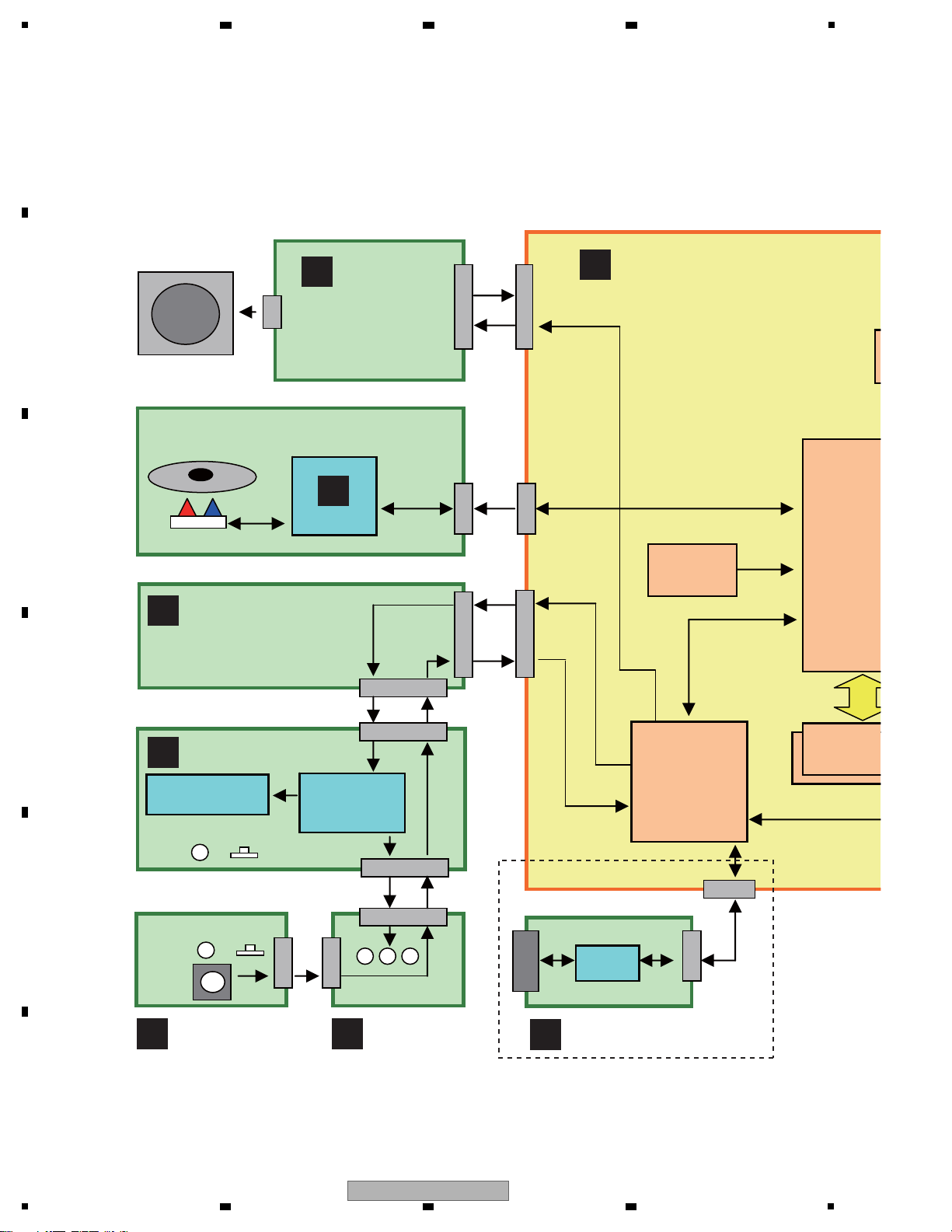
4. BLOCK DIAGRAM
4.1 OVERALL WIRING DIAGRAM
A
B
C
D
E
F
18
1
2 3 4
BDP-LX54
Page 19
5
D: OWZ9016)
4)
-
When ordering service parts, be sure to refer to "EXPLODED VIEWS and PARTS LIST" or "PCB PARTS LIST".
-
The > mark found on some component parts indicates the importance of the safety factor of the part.
Therefore, when replacing, be sure to use parts of identical designation.
-
: The power supply is shown with the marked box.
MM
M
GND
3.3V
EEP_WP
EEP_SCL
EEP_SDA
SL1+
SL1-
SL2-
SL2+
GND
SPIN_U
SPIN_V
SPIN_W
COMMON
GND
LDG_SW
LDM+
EJ_SW
LDM-
GND
EXP_BEXP_B+
EXP_AEXP_A+
TD
TR
FR2
FD2
FR1
FD1
V5PD
A
D
C
B
GNDPD
RF+
RF-
GNDPD
GNDPD
E
G
VREFPD
F
H
NC
NC
TEMP
OEIC_SW1
OEIC_SW2
SDIO
SCLK
SEN
LDDENB
VMON
GNDO
VO5V
GNDO
GNDO
VO7V
SC3002
1
2
345
6
7
8
9
1011121314151617181920
SC3001
1
2
3
4
5
6
7
8
9
10
11
12
13
14
15
16
17
18
19
20
21
22
23
24
25
26
27
28
29
30
31
32
33
34
35
36
37
38
39
40
123456789
1011121314151617181920
CN1
1
2
3
4
5
6
7
8
9
10
11
12
13
14
15
16
17
18
19
20
21
22
23
24
25
26
27
28
29
30
31
32
33
34
35
36
37
38
39
40
CN101CN104
CN102
1
2
3
4
CN103
1
2
3
4
1
2
3
4
5
6
7
8
1
2
3
4
5
6
7
8
VIDEO HDMI
J7202
Y
PB L
PR
R
LAN(10/100)
/USB
OPTICAL
SLED
MOTOR
SPINDLE
MOTOR
LOADING
MOTOR
SL1+
SL1-
SL2-
SL2+
SPIN_W
SPIN_V
SPIN_U
COMMON
GND
LDM-
EJ_SW
LDM+
LDG_SW
J7001
SC2701
J2202
NC
NC
NC
I
BRIDGE ASSY
BD DRIVE BD6P S (OXX8037)
Traverse Mech BD6P
6 7 8
A
B
C
D
E
F
5
BDP-LX54
6 7 8
19
Page 20
1
B
Loader
FRONT
CON
FL CON
FL
FAN
BDP-LX54, BDP-43FD, BDP-41FD ONLY
SDRA
DDR3
CEC
PLL
Driver
IR
LED
LED
SW
LED
SW
POWER ASSY
(POWER PWB-S)
H
232C ASSY
G
LEDB ASSY
E
KEYB ASSY
F
FLKB PWB-S
B
MTFB ASSY
C
BRIDGE ASSY
I
MAIN PWB-S
A
2 3 4
4.2 OVERALL BLOCK DIAGRAM
A
B
C
D
E
F
20
1
2 3 4
BDP-LX54
Page 21
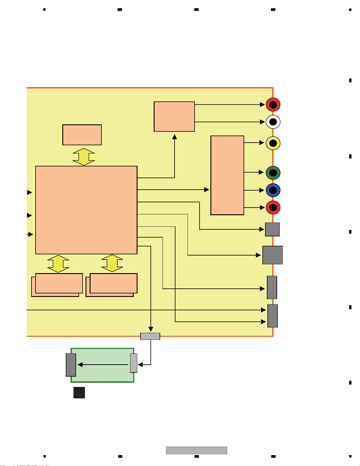
BROADCOM
BCM7633
Video
Driver
LAN
USB
HDMI
Audio
DAC
OPTICAL
DDR3
SDRAM
SDRAM
DDR3
NAND
Flash
CEC In/Out
USB
USBB ASSY
D
5
6 7 8
A
B
C
D
E
F
BDP-LX54
5
6 7 8
21
Page 22
1
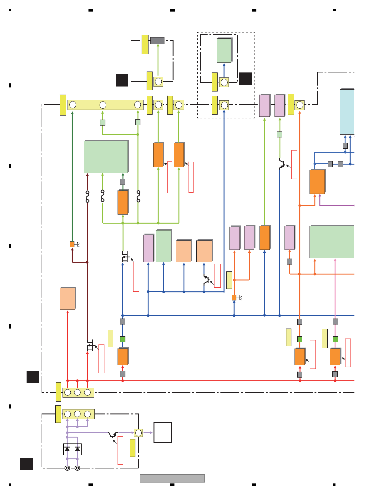
+12V
AT_12V
P9001
IC7208
BCM7633
2
3
CN901
IC2503
PST8246N
Reset IC
Q9014
RTQ035P02
DRIVE_12V
DRIVE_P-CON
IC3003
AZ1117HA
VO7V
IC9004
AOZ1016
L9004
AT_5V
IC2505
TC7SET08F1E
IC2504
IXC893WJQZ
SUB MICOM
IC2501
PST8431N
Reset IC
IC2502
PST8220N
Reset IC
KEY_STBY
Q9012
RTQ035P02
DRIVE_P-CON
DRIVE_5V
IC7209
MP62055
1
to PICKUP
IC7202
PQ1LAX95
IC7204
LCX125FT
MAIN_P-CON
D_5V
L7205
J7202
GP1F55T
D_1.2V
5.216V
DCDC
Conv.
10uH
DCDC
Conv.
IC9001
MP28254
L9001
4.7uH
1.215V
MAIN_P-CON
DCDC
Conv.
IC9002
AOZ1016
MAIN_P-CON
L9002
10uH
3.336V
3.422V
D_3.3V
IC7802
EDJ1108DBSE-DJ-F
DDR3
R7812
R7813
SC7201
HDMI
4
Q7202
2SA1530AR
Q2502
2SC3928AR
AT_12V
D952
7
8
F3003
2A
IC3001
R2A30222
FTS Driver
10uH
R7854
0
F7808
47
F3002
2A
F3001
L3002
4.7uH
V5PD
11
37
VO5V
L3001
4.7uH
40
VO7V
IC7201
PCA9517
IC7207
MP62055
CN7201
J7201
7
2
to MECHA
1
CN501
JA501
USB&LAN
Terminal
OPTICAL OUT
Terminal
1
P2501
SC3002
1
P4701
IC4701
M3221EIP
RS232C
HDMI
Terminal
IC7203
MP62055
FB9007
FB9008
FB9001
FB
9002
FB9003
FB
9004
AT_5V
USB
Terminal
USB1_PWRON
MAIN_P-CON
FAN
1
CN902
IC7801
BD3539FV
M_5V
IC3002
BA10358F
X7202
VCXO
FB7205
0.5A
R3087
22
VTT
F_AT_5V
SC3001
2
3
4
POWER ASSY
(POWER PWB-S)
H
232C ASSY
G
USBB ASSY
D
MAIN PWB-S
A
USB0_PWRON
BDP-LX54,
BDP-43FD,
BDP-41FD
ONLY
2 3 4
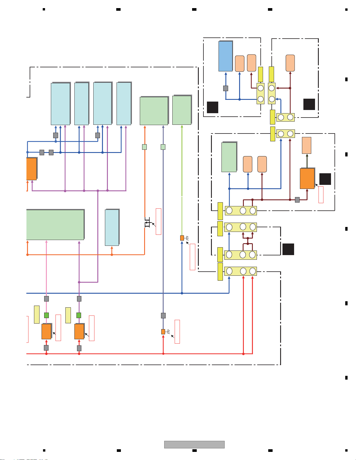
4.3 POWER SUPPLY BLOCK DIAGRAM
A
B
C
D
E
F
22
1
2 3 4
BDP-LX54
Page 23
IC7208
BCM7633
IC7803
EDJ1108DBSE-DJ-F
DDR3
SUB_P-CON
IC9003
MP2303A
L9003
D_1.5V
D_1.2V
MAIN_P-CON
1.52V
4.7uH
DCDC
Conv.
IC9001
MP28254
L9001
4.7uH
1.215V
MAIN_P-CON
MAIN_P CON
IC7802
EDJ1108DBSE-DJ-F
DDR3
IC7804
EDJ1108DBSE-DJ-F
DDR3
IC7805
EDJ1108DBSE-DJ-F
DDR3
R7812
R7813
IC7806
SUMSANG
2Gb NAND Flash
IC2201
PQ1LA335
MAIN_P-CON
IC2202
WM8524
Audio DAC
AUDIO_3.3
SUB_PC_-5V
16
IC301
GP1UE28RK0VP
Remote Sensor
IC201
PDC182
FL Driver
LED×1
R301
0
V+5E
CN201CN2501
AT_5V
IC9007
PQ1CZ41H
SUB_PC_3.3V
L2202
100uH
R7854
0
F7808
47
47
Q9021
RTQ035P02
11
12
LED×1
JP301
1 8
LED×5
CN402
1
8
1
6
1
6
CN401
JP201
DCDC
Conv.
Discreet
FL
13
2
4
V+12V
V+5E
V+12V
FLDC+
FLDC-
-23V
FLOFF
CN201 CN602
2
4
13
16
11
12
V+5E
V+12V
AT_12V
AT_12V
KEY
SUB_P-CON
L2201
KEY
L101
22uH
V+5E
V+12V
FB9001
FB
9002
FB9005
FB
9005
IC2301
MM1797CV
Video Driver
V+5E
V+12V
IC7801
BD3539FV
R7814
R7815
FB9014
DCDC
Conv.
100uH
MTFB ASSY
C
FLKB PWB-S
B
LEDB ASSY
E
KEYB ASSY
F
5
6 7 8
A
B
C
D
E
F
BDP-LX54
5
6 7 8
23
Page 24
1
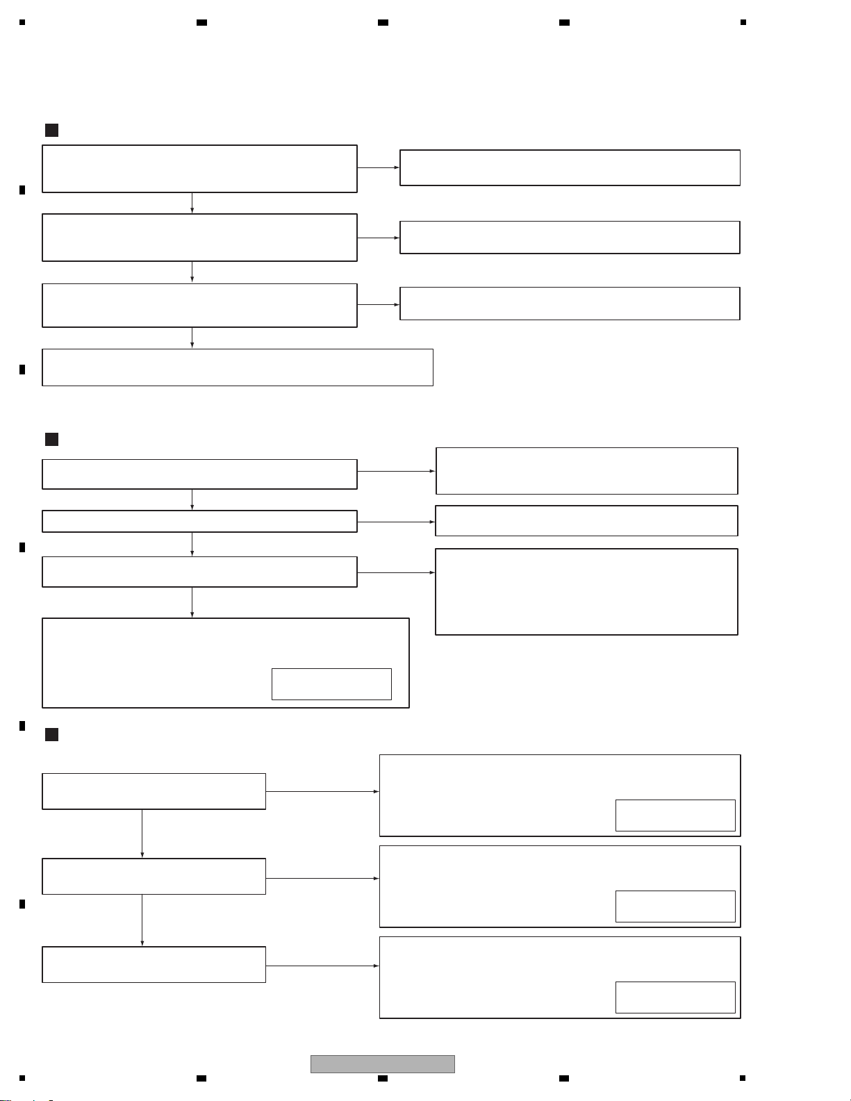
Is the 12V power supplied to pins (2, 3 and 4) of P9001 inside
MAIN PWB-S (AT_12V) while AC is ON and the power source
is OFF?
Disconnect the P9001 connector on the MAIN PWB-S after
turn the power off, then do not pins 2 and 5 of P9001 on the
MAIN PWB-S short-circuit?
Is the 12V power supplied to pins (2, 3 and 4) of CN901
on the POWER Assy (AT_12V) while AC is ON and the power
source is OFF?
Check between CN901 on the POWER Assy and P9001 on the MAIN PWB-S
and their peripheral circuits. (e.g. nearly detached connector, disconnection)
Yes
Yes
No
No
Yes
No
Yes
[1] POWER Assy (POWER PWB-S)
[2] DRIVE Assy
Replace and check the MAIN PWB-S.
(Short-circuit is being caused in the MAIN PWB-S.)
Replace and check the POWER Assy. (The circuit up to 12 V
generation in the POWER Assy has broken down.)
The POWER Assy is normal. (12V power is supplied.)
Replace and check MAIN PWB-S.
Does SLED motor initialize while the
power is ON?
Does it load?
Does the spindle revolve when a disc is
inserted?
No
Yes
No
Yes
No
Does the problem (discs cannot be played back stably)
happen only to certain discs?
Does the problem happen only to BD, DVD or CD?
Is the error rate wrong?
No
No (The problem happens to all discs.)
No
1 Check the drive relay board (BRIDGE Assy) and circuits
around CN101 and CN104.
Check any connector nearly detached or obliquely inserted.
Check any disconnected pattern etc.
2 Replace and check MAIN PWB-S.
3 Replace and check BD drive.
1 Check the drive relay board (BRIDGE Assy) and circuits
around CN101 and CN104.
Check any connector nearly detached or obliquely inserted.
Check any disconnected pattern etc.
2 Replace and check MAIN PWB-S.
3 Replace and check BD drive.
(In case LD breakdown etc. causes the problem)
Replace and check BD drive.
(In case the problem derives from PU breakdown or
disc-related factors)
1 Check any dirt on discs
2 Check whether the problem is disc-specific
(e.g. Pirated edition)
3 Replace and check BD drive
(In case discs cause the problem)
1 Check any dirt on discs.
2 Check whether the problem is disc-specific.
MAIN PWB-S is likely
to have broken down.
MAIN PWB-S is likely
to have broken down.
1 Check the drive relay board (BRIDGE Assy) and circuits
around CN102 and CN104.
Check any connector nearly detached or obliquely inserted.
Check any disconnected pattern etc.
2 Replace and check MAIN PWB-S.
3 Replace and check BD drive.
MAIN PWB-S is likely
to have broken down.
1 Check the drive relay board (BRIDGE Assy) and circuits
around CN103 and CN104.
Check any connector nearly detached or obliquely inserted.
Check any disconnected pattern etc.
2 Replace and check MAIN PWB-S.
3 Replace and check BD drive.
MAIN PWB-S is likely
to have broken down.
(SLED is not
operating)
(It is not loading)
(The spindle
motor is not
revolving)
Yes
Yes
Power does not come ON.
BD drive does not operate properly.
Discs cannot be played back stably.
2 3 4
5. DIAGNOSIS
5.1 DIAGNOSIS FLOWCHART
A
B
C
D
E
F
24
1
2 3 4
BDP-LX54
Page 25
5
The following problems do not always suggest a defect or malfunction of this Player.
Refer to the problems and lists of possible solutions below.
Power
The Player power cannot be turned on. • Is the power cord firmly plugged into the AC outlet?
• When the power cord is plugged into an AC outlet, press and hold u SANDBY/ON on the
Player until "RESET" appears on the front panel display.
The power will be automatically turned off. Then turn on power again.
The Player power is turned on
automatically.
• When "Settings" – "control function setting" is set to "Yes" on the player, the player’s power
may turn on when the connected TV is operated.
The Player power is turned off
automatically.
• Is "Auto Power Off" set to "Yes"? When "Auto Power Off" is set to "Yes", the power will be
automatically turned off after 10 continuous minutes of inactivity (no playback).
• When "Settings" – "control function setting" is set to "Yes" on the player, the player’s power
may turn off when the power of the connected TV is turned off.
Basic Operation
The remote control does not work. • Use the remote control within its operating range.
• Replace the batteries.
Cannot operate the Player. • Are you operating the Player within the specified operating temperature range?
Disc Playback
The Player cannot play a disc. • Take out the disc and clean it.
• Make sure that the disc is loaded properly (aligned in disc tray and label-side up).
• Make sure that region code on the disc matches that of this Player.
• Allow any condensation in or near the Player to dry.
• Check that the disc is recorded in the compatible TV system (PAL or NTSC).
• The Player cannot play back video which was not recorded normally.
• Proper playback may be impossible due to the state of the disc recording, a scratched,
warped or dirty disc, the state of the pick-up, or compatibility issues between this Player
and the disc being used.
• When the recorded time of a disc is unusually short, playback may not be possible.
• BD-RE/-R discs recorded in a format other than BDMV/BDAV cannot be played back.
The disc is automatically ejected after
closing the disc tray.
• Make sure that the disc is loaded properly (aligned in disc tray and label-side up).
• Take out the disc and clean it.
• Make sure that region code on the disc matches that of this Player.
• Make sure that the disc is playable.
.spotsoediV • Has the Player been subjected to shock or impact? Are you using it in an unstable location?
The Player will stop if it senses shock or vibration.
The Player makes a snapping sound
when starting playback or loading a disc.
• The player may sometimes make a snapping sound when starting playback if it has not been
operated in a while. These sounds are not malfunctions of the player but are normal operating
conditions.
[1] T roubleshooting Table
Problem Possible causes and solutions
Problem Possible causes and solutions
Problem Possible causes and solutions
6 7 8
5.2 TROUBLESHOOTING
A
B
C
D
5
BDP-LX54
6 7 8
E
F
25
Page 26

1
Picture
No picture. • Make sure that the cables are connected correctly.
• Make sure that the connected TV or the AV receiver is set to the correct input.
• Take out the disc and clean it.
• Make sure that region code on the disc matches that of this Player.
• There is no picture from the HDMI output.
− Are the settings performed correctly? Please check the settings.
• There is no picture from the component video output.
− Are the settings performed correctly? Please check the settings.
Screen freezes and operation
buttons do not work.
• Press g STOP, then restart playback.
• Turn off the power and turn on the power again.
• If the power is not turned off, perform a reset.
• Is the disc damaged or dirty? Check the condition of the disc.
There is just audio with no video. • Is the connection cable for video output connected properly?
Widescreen video appears vertically
stretched, or black bands appear at
the top and bottom of the screen.
• Is "TV Aspect Ratio" set to match the connected TV?
• If you are using a widescreen TV, is the "TV Aspect Ratio" set to "Wide"?
Square noise (mosaic) appears on
the screen.
• Blocks in images may be visible in scenes with rapid movement due to the characteristics
of digital image compression technology.
The playback screen will be
disturbed if DVD video is recorded
to a VCR, or played back through a
VCR.
• This Player complies with analog copy protection. Some discs contain a copy prohibiting
signal. If you try to play back such discs through a VCR, or record to a VCR and play back
the signal, the copy protection will prevent normal playback.
Audio is not output, or images are
not played back properly.
• The audio may not be output or the images may not be played back properly for some discs
in which copyright-protected contents are recorded.
Images of played-back 3D discs
do not appear to be in 3D.
• Connect this player and the TV, using a High Speed HDMI cable.
• Check if the 3D Mode setting of this player is set to 2D.
If it is set to 2D, even played-back images of a Blu-ray disc that supports 3D will not appear
to be in 3D on a TV that supports 3D.
• If played-back images of only a particular disc do not appear to be properly in 3D, check the
3D effects of this player with other 3D discs.
Three-dimensional effects of discs may differ from disc to disc.
• For 3D display of 3D materials that have been recorded in the Side-by-Side system, the 3D
setting is also required on the customer's TV. Request the customer to confirm the 3D setting
of the TV.
• When an AV amp is connected between this player and the TV, that AV amp is required to
support 3D. Request the customer to confirm the specifications and settings of his/her AV amp.
Sound
No sound, or sound is distorted. • If the volume of the TV or amplifier is set to minimum, turn the volume up.
• There is no sound during still mode, slow motion playback, fast forward and fast reverse.
• DVD audio recorded in DTS is only output from the DIGITAL OUT OPTICAL terminal.
Connect a DTS compatible digital amplifier or decoder to the DIGITAL OUT OPTICAL
terminal on this Player.
• Check that the audio cable is connected correctly.
• Check that the cable plugs are clean.
• Take out the disc and clean it.
• Audio may not be output depending on the audio recording status, such as when audio other
than an audio signal or non-standard audio is recorded for the audio content of the disc.
Left and right channels of audio are
reversed, or sound comes out of
only one side.
• Are left and right audio cables connected to the opposite terminal, or is one side
disconnected?
Audio is not output, or images are
not played back properly.
• The audio may not be output or the images may not be played back properly for some discs
in which copyright-protected contents are recorded.
Problem Possible causes and solutions
Problem Possible causes and solutions
A
2 3 4
B
C
D
E
F
26
1
2 3 4
BDP-LX54
Page 27

5
Cannot download BD-LIVE contents. • Is the LAN cable connected properly?
• Is the USB memory device properly connected? Check that the USB memory device is
connected to the BD STORAGE/SERVICE terminal of this Player.
• Check if the BD disc supports BD-LIVE.
• Check the setting for "BD Internet Access".
Control function Setting
Control function wiht HDMI does not
work.
Other
The TV operates incorrectly. • Some TVs with wireless remote control capability may operate incorrectly when using the
remote control of this Player. Use such TVs away from this Player.
The Player heats up during use. • When using this Player, the console cabinet may heat up depending on the usage
environment. This is not a malfunction.
Input of connected TV and AV
system switches automatically.
• When "Settings" – "control function setting" is set to "Yes" on the player, the input on the
connected TV or AV system (AV receiver or amplifier, etc.) may switch automatically.
• KEY LOCK is in effect. Depress the remote control unit's KEY LOCK button for five seconds
or more to cancel the KEY LOCK function.
The display panel shows " HOLD ",
and operations are disabled.
• Connect the HDMI cable properly.
• Use High Speed HDMI™ cables when using the control function with HDMI.
The control function with HDMI may not operate properly if other HDMI cables are used.
• Set "Settings" – "control function setting" on the player to "Yes".
• The control function with HDMI does not work with devices of other brands, even if connected
using an HDMI cable.
The control function with HDMI will not work if devices that do not support the control function
with HDMI or devices of other brands are connected between the control function with HDMI compatible device and the player.
It may also not work with certain Flat Panel TVs.
• Set control function with HDMI to On on the connected device.
The control function with HDMI works when control function with HDMI is set to On for all
devices connected by HDMI cable. Once connections and the settings of all the devices are
finished, be sure to check that the player’s picture is output to the Flat Panel TV. (Also check
after changing the connected devices and reconnecting HDMI cables.) The control function
with HDMI may not operate properly if the player’s picture is not properly output to the Flat
Panel TV.
• The control function with HDMI may not work if three or more players, including this player,
are connected.
• Also refer to the operating instructions of the connected device.
Problem Possible causes and solutions
Problem Possible causes and solutions
Network
Cannot connect to the Internet. • Is the LAN cable connected properly?
• Is the wrong cable such as a modular cable used? Connect a LAN cable to the LAN terminal.
• Is the power for the connected equipment, such as broadband router or modem turned on?
• Is the broadband router and/or modem properly connected?
• Is the proper value(s) set in the network setting? Check "Communication Setup".
Problem Possible causes and solutions
6 7 8
A
B
C
D
E
F
BDP-LX54
5
6 7 8
27
Page 28

1
Messages Relating to BD disc and DVD disc
Error Message Possible Error Suggested Solution
Cannot play. • The disc cannot be played back with this
Player.
• Check the disc, and load it correctly.
Incompatible disc. • If you load a disc which cannot be played
with this Player (i.e. a scratched disc), or if
you load a disc upside down, this message
will appear, and the disc tray will automatically
pop out.
• Occurs if the loaded disc cannot be played
because it is a non-standard disc or
scratched, etc.
• Remove the disc.
Cannot operate. • Occurs if an operation is incorrect. —
This USB memory is not formatted
properly. Please format the memory in
USB memory management.
• Occurs if there is a formatting error. • Format the USB memory again.
The Connected USB Memory cannot
be used. It should be compliant with
USB 2.0.
• Occurs if USB memory not compliant with
USB 2.0 High Speed (480Mbit/s) is used
(i.e. USB 1.0/USB 1.1).
• Connect USB 2.0 High Speed
(480Mbit/s) compliant USB memory.
• The following messages appear on the TV screen in case the disc you tried to playback is not appropriate or the operation
is not correct.
Messages Relating to FAN MOTOR
• When FAN motor is abnormal, the unit return to standby mode, if the below message appear on the screen,
check the FAN motor and the FAN motor control circuit
[2] On-screen Error Messages
To Reset this Player
• If this Player receives strong interference from a source such as excessive static electricity, strong external noise,
malfunction of power supply, or voltage caused by lightning during use or a wrong operation is sent to the Player, errors like
the Player not accepting an operation may occur. Press and hold u STANDBY/ON on the Player until "RESET" appears on
the front panel display when the Player does not operate properly even after the power has been turned off. Then turn on the
power again.
• It may take several minutes until completion as the system check will be executed when the power is turned ON.
Please wait until the indicator lights up in this case.
• Since all settings including the language setting stored in memory are also reset when a reset has been performed, they
must be set again.
• When the problem persists even after performing a reset, unplug the AC cord and plug it in again. If this does not solve the
problem, contact the nearest service center approved by Pioneer.
The Fan On the Rear Panel May Not Be Working Correctly, Check The Fan
Error Message
FAN ERR
Main FL Display Unit
* The fan used in this product starts its rotation at the same time as the power is turned on and stops as the
power is turned off. It is not controlled by temperature etc.
A
2 3 4
B
C
D
E
F
28
1
BDP-LX54
2 3 4
Page 29

5
To confirm the model name, region number, and drive version, or to reset to the factory default settings, proceed as follows:
Turn on the unit then press the REP_A key on the remote control unit for service (GGF1067). The MAIN TEST MENU screen
shown below will be displayed:
For operation of the MAIN TEST MENU screen, use the remote control unit supplied with this unit. Confirm on the screen that
the settings are proper.
To reset to factory default, proceed as follows:
1. Select "SHIP" then "ON" on the menu, using the [i/j/k/l] key on the supplied remote control unit, then press the
ENTER key.
2. The unit automatically turns off and on. The On Screen Language setting screen is displayed, as shown below.
Select the language.
1 MODEL: Model name and region
2 Region CK | BD/DVD: Region No.
3 BD Drive Ver.: Version of the drive
4 SHIP: For resetting to the factory default
(The SHIP setting item is also provided on the User menu. For details, refer to the operating instructions of the unit.)
For operation, use the [i/j/k/l] key and OK key on the supplied remote control unit.
1
2
3
4
6 7 8
6. SERVICE MODE
6.1 INFORMATION SCREEN DISPLAY AND THE FACTORY DEFAULT SETTINGS
A
B
C
D
E
F
BDP-LX54
5
6 7 8
29
Page 30

1
Necessary Items
• USB memory device (one having an access lamp is preferable)
• Files for error-rate measurement (BDP430_ER.ZIP)
(Download the above zip folder from Niis then unzip it.)
1 Place the two files in a folder indicated below in the root directory of the USB memory device.
(NEVER place a folder, such as the "in" folder, in the root directory.)
Three types of files are provided: those for measuring the inner track, middle track, and outer track.
Depending on the track you wish to measure, copy the files in the corresponding folder into the USB memory device.
These files can be used for measuring error rates of both a DVD and BD.
A medium to be measured will be automatically distinguished.
For measurement of error rates for the inner track, use the following files in the "in" folder:
• BDP430_Measure_Error_in
• BrcmLstaTrigger
For measurement for the middle track, use the following files in the "mid" folder:
• BDP430_Measure_Error_mid
• BrcmLstaTrigger
For measurement for the outer track, use the following files in the "od" folder:
• BDP430_Measure_Error_od
• BrcmLstaTrigger
2 With the unit's power off, plug the USB memory device into the USB port on the front or rear panel of the unit.
3 Turn on the unit.
4 A test will start automatically.
The message indicating that a test is in progress will be displayed.
The tray opens automatically. Load a disc whose error rates you wish to measure on the tray then close it manually.
5 The tray will open after 10 to dozens of seconds. Remove the disc then close the tray manually.
(Error rates will only be displayed after the tray is closed.)
Measurement Method
2 3 4
6.2 MEASUREMENT OF ERROR RATES
A
B
C
D
E
F
30
1
2 3 4
BDP-LX54
Page 31

5
6 The error rates will be displayed on the screen. (The judging criteria are described in the next item.)
Nearly simultaneously, the results of error rate measurement will be written in the USB memory device as a text file.
(Example of the name of a text file when measuring error rates for the outer track: [result_od_00e036d61ffa.txt])
7 After confirming that writing to the USB memory device has been completed with its access lamp, turn the unit off then
unplug the USB memory device. (If a USB memory device not having an access lamp is used, turn the unit off about
5 seconds after the results of measurement are displayed.)
To perform error rate measurement again, repeat the steps from 1.
In such a case, the results of a later measurement will be written over the existing data in the USB memory device.
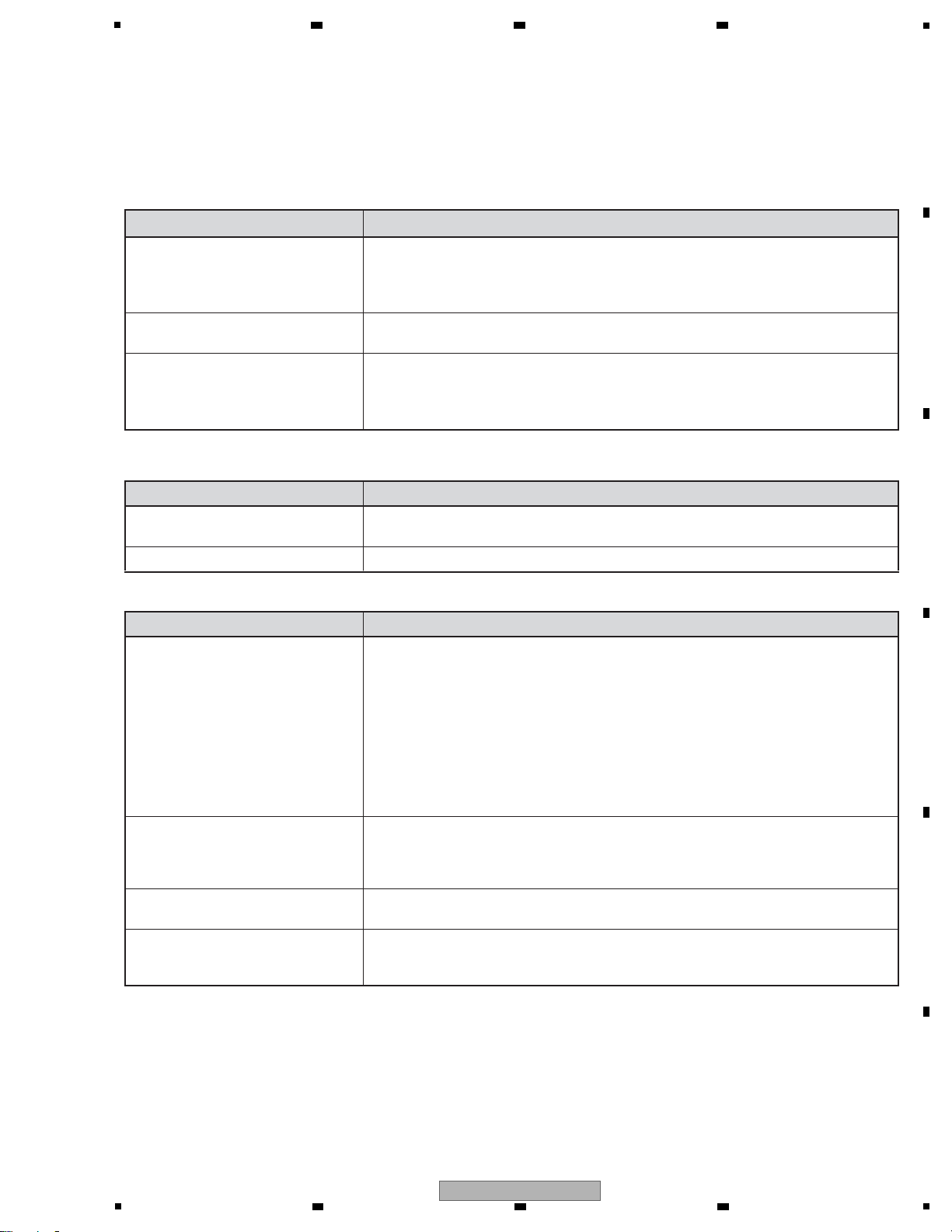
Max Uncorrectable Allowed:
→ Average correctable error counts (reference value)
(The indication on the screen is wrong.)
Max Correctable Allowed:
→ Maximum correctable error counts (reference value)
Maximum Uncorrectable:
→ Not in use
Maximum Correctable:
→ Maximum correctable error counts (measured value)
Average Uncorrectable:
→ Not in use
Average Correctable:
→ Average correctable error counts (measured value)
Test Status: If the measured average/maximum correctable error counts are less than or equal to the
reference values, "Pass" will be indicated.
If any measured value exceeds the above-mentioned reference value, "Fail" will be indicated.
Indication of
measured value
0
0
Indication of
measured value
(Not in use)
DVD
38
200
(reference value)
BD
220
1000
0
(reference value)
(reference value) (reference value)
Indication of
measured value
0
Indication of
measured value
(Not in use)
(Not in use) (Not in use)
Descriptions of Results
6 7 8
A
B
5
6 7 8
BDP-LX54
C
D
E
F
31
Page 32

1
1
2
2
2
1
1
4
5
2
3
3
(1) Remove the two screws of the side.
(LX-HZA056WJF9)
(2) Remove the three screws of the rear.
(LX-JZA010WJF7)
(3) Slide the top cab Assy-S to the rear side and
remove it.
[1] Tray Panel Section
[1-1] Top Cab Assy-S
(1) Press the u STANDBY/ON button to turn on
the power.
(2) Press the h OPEN/CLOSE button to open
the tray.
(4) Press the h OPEN/CLOSE button to close the
tray.
(5) Press the u STANDBY/ON button to turn off
the power.
(3) Remove the tray panel section to the upper
side.
[1-2] Tray panel section
Top Cab Assy-S
Tray panel section
• Rear view
Note:
(1) Do NOT look directly into the pickup lens. The laser beam may cause eye injury.
(2) Even if the unit shown in the photos and illustrations in this manual may differ from your product, the
procedures described here are common.
4
2
2 3 4
7. DISASSEMBLY
A
B
C
D
E
F
32
1
BDP-LX54
2 3 4
Page 33

5
2
2
2
2
2
(1) Disconnect the one flexible cable on the
MTFB Assy. (CN602)
(2) Unhook the seven hooks and remove the front
panel section.
[2] Front Panel Section
Front panel section
• Bottom view
When the tray cannot be opened because the
power cannot be turned on, it can be opened
using the emergency disc ejection rod
(GGF1529). (A long, thin rod about 1 mm in
diameter can be used in place of the rod.)
Bend the emergency disc ejection rod at aright
angle, and insert it horizontally into a hole as
shown in the figure.
• How to open the tray when the power cannot be turned on
Center angle LX
BDP-LX54, BDP-43FD BDP-430, BDP-41FD
2
2
2
1
MTFB Assy
Front panel section
CN602
Emergency disc ejection rodEmergency disc ejection rod
Emergency disc
ejection rod
6 7 8
A
B
C
D
E
BDP-LX54
5
6 7 8
F
33
Page 34

1
(1) Remove the five screws and remove the
center angle LX. (LX-JZA010WJF7)
[3] BD DRIVE BD6P S
[3-1] Center Angle LX (BDP-LX54, BDP-43FD only)
(1) Remove the two screws. (LX-BZA148WJF7)
(2) Remove the two screws. (LX-JZA010WJF7)
(3) Remove the two screws. (LX-JZA010WJF7)
(BDP-LX54, BDP-43FD, BDP-41FD only)
(4) Remove the four screws of the BD DRIVE
BD6P S. (LX-JZA033WJF7)
[3-2] BD DRIVE BD6P S
1
1
1
1
1
4
4
4
4
1
2
3 3
2
1
BD DRIVE BD6P S
BDP-LX54,
BDP-43FD,
BDP-41FD
ONLY
Center Angle LX
• Rear view
1
A
B
2 3 4
C
D
E
F
34
1
BDP-LX54
2 3 4
Page 35

5
Hook
(5) Remove POWER-MAIN wire wire from the
hook of insulation holder to the upper side.
(6) Stand the BD DRIVE BD6P S in the arrow
direction of the figure.
(7) Reconnect the flexible cable of the front panel
section to the MTFB Assy. (CN602)
Diagnosis
5
Insulation holder
POWER-MAIN wire
6
BD DRIVE BD6P S
BD DRIVE BD6P S
-1
6
-2
POWER Assy
(POWER PWB-S)
7
MTFB Assy
MAIN PWB-S
Front panel section
CN602
6 7 8
A
B
C
D
E
5
6 7 8
BDP-LX54
F
35
Page 36

1
(1) Remove the acetate cloth tape.
(2) Remove the aluminum tape. (VEF1067)
(3) Remove the aluminum tape. (VEF1067)
(4) Remove the one screw. (LX-JZA010WJF7)
(5) Remove the USBB Assy.
Note:
After replacing the USBB Assy, put the aluminum
tapes and acetate cloth tape on the same position.
[4] USBB Assy
USBB Assy
USBB Assy
USBB Assy
Aluminum tape
Aluminum tape
Acetate cloth tape
1
2
5
3
4
A
B
2 3 4
C
D
E
F
36
1
BDP-LX54
2 3 4
Page 37

5
Cleaning the Pickup Lenses
(1) Remove the six screws.
(2) Unhook the three hooks and remove the top
cover.
[1] T op Cover
Clean the pickup lenses when it is stained, using
the following cleaning materials:
Cleaning liquid : GEM1004
Cleaning paper: GED-008
Caution:
The pickup for Blu-ray is a high-precision
component; therefore, clean the lens with
enough care so as not to cause a misalignment
in the optical axis.
After cleaning the lens, make sure that the error
rate is below the reference value.
Top cover
1
1 1
2
2
2
2
1 1
1
Pickup lenses
Front
Front
Front
• Bottom view
6 7 8
A
B
C
D
E
5
BDP-LX54
6 7 8
F
37
Page 38

1
Exchange the DRIVE Assy
Firmware update
None
None
None
When Adjustment Points
[1] Exchange the DRIVE Assy
Note : Be sure to update the firmware before starting adjustments or settings.
Mechanical
point
Electric
point
Exchange the
MAIN PWB-S
When Adjustment Points
[2] Exchange MAIN PWB-S
Mechanical
point
Electric
point
After the MAIN PWB-S is replaced, be sure to update the firmware before starting any adjustment/setting.
Note: If firmware updating is not performed after the MAIN PWB-S is replaced,
the device may not work properly.
2 3 4
8. EACH SETTING AND ADJUSTMENT
8.1 NECESSARY ITEMS TO BE NOTED
A
B
C
D
8.2 UPDATING OF THE FIRMWARE
E
F
38
1
2 3 4
BDP-LX54
Page 39

5
Start
Turn the power on.
No
Yes
Updating Procedure
Note: Be sure to update the firmware after the MAIN PWB-S is replaced.
(Updating can also be performed using the User menu. For details, refer to the operating instructions of the unit.)
1. Press [STANDBY/ON] button to turn the switch on, then wait till the BD/DVD/CD disc indicator changes from blinking to lit.
2. Press [OPEN/CLOSE] button to open the Tray, put the update disc on the tray and close the tray.
3. The updating with the disc will start.
4. During the updating, "NOW UPDATING DO NOT UNPLUG AC CORD" appears on the monitor screen.
And the version updating progress bar is displayed.
5. When updating with the disc is completed, the Tray automatically opens.
6. When the updating is completed, the following appears on the monitor screen. : "Success, Please remove the disc..."
If the version updating fails, take out the disc, turn off the power and take the procedure again starting from [1] above.
7. Remove the disc from the Tray and press [ENTER], then the Tray will close and the power will automatically turn off and on.
* If the front-end software was updated, start updating front-end software at this point. Please follow the procedure
described on the screen.
8. Check the version on [HOME MENU] - [SETTINGS] - [VERSION].
If the version is not updated, take the procedure again from Step [2].
Note: Do not unplug the AC cord during version updating.
Restart
The updating starts.
Open the tray, put the update disc
and close the tray.
The tray opens automatically.
Monitor:
"Success, Please remove the disc..."
Check the version.
Updating successful.
Remove the disc and push [ENTER].
(Automatically turns off and on.)
Monitor displays the update failure
message.
Updating unsuccessful.
End
Remove the disc
and turn the power off.
Updating completed
6 7 8
A
B
C
D
E
5
BDP-LX54
6 7 8
F
39
Page 40

1
NOTES: - Parts marked by “NSP” are generally unavailable because they are not in our Master Spare Parts List.
-
The > mark found on some component parts indicates the importance of the safety factor of the part.
Therefore, when replacing, be sure to use parts of identical designation.
-
Screws adjacent to b mark on product are used for disassembly.
-
For the applying amount of lubricants or glue, follow the instructions in this manual.
(In the case of no amount instructions, apply as you think it appropriate.)
or or or or
BDP-43FD/UCXV,
BDP-430/UCXVSM
only
2 3 4
9. EXPLODED VIEWS AND PARTS LIST
A
9.1 PACKING SECTION
B
C
D
E
F
40
1
2 3 4
BDP-LX54
Page 41

5
6 7 8
(1) PACKING SECTION PARTS LIST
Mark No. Description Part No.
> 1 AC Cord See Contrast table (2)
2 Video / Audio Cable VDE1077
3 Remote Control Unit See Contrast table (2)
4 Battery Door AZN8047
NSP 5 Dry Cell Battery (R03, AAA) VEM1051
6 Operating Instructions See Contrast table (2)
7 Operating Instructions See Contrast table (2)
8 Operating Instructions See Contrast table (2)
9 Operating Instructions See Contrast table (2)
10 Operating Instructions See Contrast table (2)
A
NSP 11 Warranty Card See Contrast table (2)
NSP 12 UC Label See Contrast table (2)
NSP 13 Serial Label S VRW2188
14 Polyethylene Bag VHL1088
15 Front Pad OHA8036
16 Rear Pad OHA8037
17 Packing Case See Contrast table (2)
NSP 18 HOSO-PP DHL1184
(2) CONTRAST TABLE
BDP-LX54/YXV5, SXV, BDP-43FD/UCXV, BDP-430/UCXVSM, YXV5, SXV and BDP-41FD/UCXV are constructed the same
except for the following:
Mark No. Symbol and Description
1 AC Cord ADG7062 ADG7062 ADG7061 ADG7022 ADG1154 ADG1154 ADG7022
>
3 Remote Control Unit VXX3385VXX3385 VXX3386VXX3383 VXX3382 VXX3382 VXX3383
6 Operating Instructions (En) VRB1529 VRB1529 Not used Not used VRB1529 VRB1529 Not used
7
Operating Instructions
(Fr, De, It, Nl, Es)
8 Operating Instructions (Ru)Not used VRC1577 Not used Not used Not used VRC1577 Not used
BDP-LX54
/YXV5
VRE1123 Not used Not used Not used VRE1123 Not used Not used
BDP-LX54
/SXV
BDP-43FD
/UCXV
BDP-430
/UCXVSM
BDP-430
/YXV5
BDP-430
/SXV
BDP-41FD
/UCXV
B
C
D
9 Operating Instructions (En, Fr) Not used Not usedVRD1241Not used Not used Not used VRD1241
10 Operating Instructions (En, Fr, Es) Not used Not used Not used VRD1242 Not used Not used Not used
NSP 11 Warranty Card ARY7143 ARY7142 ARY7139 ARY7045 ARY7143 ARY7142 AR Y7139
NSP 12 UC Label Not used Not used ORW9024 ORW9024 Not used Not used
17
Packing Case OHG9025 OHG9027 OHG9031 OHG9018 OHG9017 OHG9020 OHG9021
Not used
BDP-LX54
5
6 7 8
E
F
41
Page 42

1
A
D
H
A
C
G
Cleaning paper :
GED-008
A
B
B
D
F
F
D
E
A
B
B
E
C
C
A
C
C
D
CONTACT SIDE
NON-CONTACT
SIDE
D
BDP-LX54,
BDP-43FD
only
BDP-LX54,
BDP-43FD
only
BDP-LX54,
BDP-43FD,
BDP-41FD
only
BDP-LX54,
BDP-43FD,
only
BDP-430,
BDP-41FD
only
Refer to
"9.3 FRONT PANEL SECTION".
BDP-LX54,
BDP-43FD,
BDP-41FD
only
BDP-430,
BDP-41FD
only
9.2 EXTERIOR SECTION
A
B
2 3 4
C
D
E
F
42
1
2 3 4
BDP-LX54
Page 43

5
(1) EXTERIOR SECTION PARTS LIST
Mark No. Description Part No.
1MAIN PWB-S See Contrast table (2)
2 • • • • •
3 MTFB Assy See Contrast table (2)
4 USBB Assy See Contrast table (2)
5POWER PWB-S See Contrast table (2)
6 7 8
No. Description Part No.
Mark
NSP 21 Heat Shield See Contrast table (2)
NSP 22 Insulation Holder DNK5778
23 Attach See Contrast table (2)
NSP 24 Chassis C ONA8171
25 Rear Panel See Contrast table (2)
A
6 232C Assy See Contrast table (2)
7 • • • • •
8 BD DRIVE BD6P S OXX8037
> 9 AC Inlet Assy See Contrast table (2)
10 FAN Motor NFANRA093WJQZ
11 MAIN-USB Wire DKP3881
12 POWER-MAIN Wire ODF9005
13 232C-MAIN Wire See Contrast table (2)
14 MAIN-MTBF FFC ODX9017
NSP 15 Silicon Sheet 20x20 OEB8014
16 Silicon Sheet 430 OEB9011
17 Insulator See Contrast table (2)
18 Insulator See Contrast table (2)
19 Layer Chassis LX See Contrast table (2)
20 Center Angle LX See Contrast table (2)
NSP 26 Earth Angle BD6P ONE8022
NSP 27 Earth Angle 2 BD6P ONE8068
28 Rubber Foot VEB1349
29 Tray Panel See Contrast table (2)
30 Tray Holder DAH2816
pring DBH1774
S
31
32 Spring Cover DNK5799
33 Top Cab Assy-S OXX9007
NSP 34 Serial Label S VRW2188
35 Aluminum Tape 8x50 (AL) VEF1067
NSP 36 Acetate Cloth Tape • • • • •
37 Screw M3x10 See Contrast table (2)
NSP 38 Screw 2.6x8 DBA1376
39 Tuner Screw (M3x2.8) LX-BZA148WJF7
40 Screw Topcab Side BK LX-HZA056WJF9
41 Screw (M3x8) LX-JZA010WJF7
NSP 42 Loader Screw LX-JZA033WJF7
B
C
(2) CONTRAST TABLE
BDP-LX54/YXV5, SXV, BDP-43FD/UCXV, BDP-430/UCXVSM, YXV5, SXV and BDP-41FD/UCXV are constructed the same
except for the following:
Mark No. Symbol and Description
1MAIN PWB-S OXX9018 OXX9034 OXX9017 OXX9014 OXX9015 OXX9031 OXX9014
3 MTFB Assy OWZ9014 OWZ9014 OWZ9014 OWZ9013 OWZ9013 OWZ9013 OWZ9013
4 USBB Assy OWZ9017 OWZ9017 OWZ9017 OWZ9016 OWZ9016 OWZ9016 OWZ9016
5POWER PWB-S Not used Not used Not used OXX9026 OXX9027 OXX9027 Not used
5POWER Assy OWZ9028 OWZ9028 OWZ9025 Not used Not used Not used OWZ9026
6 232C Assy OWZ9027 OWZ9027 OWZ9027 Not used Not used Not used OWZ9027
9 AC Inlet Assy DKP3886DKP3886 DKP3886Not used Not used Not used Not used
>
13 232C-MAIN Wire ODF9006 ODF9006 ODF9006 Not used Not used Not used ODF9006
17 Insulator DNK5830 DNK5830 Not used DNK5798 DNK5798 DNK5798 Not used
17 Decrate Leg R Not used Not used DAH2817 Not used Not used Not used DAH2817
18 Insulator DNK5830 DNK5830 Not used Not used Not used Not used Not used
18 Decrate Leg R Not used Not used DAH2817 DAH2817 DAH2817 DAH2817 DAH2817
19 Layer Chassis LX DNA1406 DNA1406 DNA1406 Not used Not used Not used Not used
20 Center Angle LX DNE1786
NSP 21 Heat Shield Not used Not used Not used DNK5650 DNK5650 DNK5650 DNK5650
23 Attach DNK5829 DNK5829 DNK5829 Not used Not used Not used Not used
25 Rear Panel ONC9008 ONC9008 ONC9008 ONC9007 ONC9007 ONC9007 ONC9009
29 Tray Panel DAH2815 DAH2815 DAH2825 DAH2815 DAH2815 DAH2815 DAH2825
37 Screw M3x10
BDP-LX54
/YXV5
LX-JZA013WJF8 LX-JZA013WJF8 LX-JZA013WJF8 LX-JZA010WJF7 LX-JZA010WJF7 LX-JZA010WJF7 LX-JZA010WJF7
BDP-LX54
/SXV
DNE
1786 DNE1786Not used Not used Not used Not used
BDP-43FD
/UCXV
BDP-430
/UCXVSM
BDP-430
/YXV5
BDP-430
/SXV
BDP-41FD
/UCXV
D
E
F
BDP-LX54
5
6 7 8
43
Page 44

1
MTFB
CN602
B
E
F
CONTACT SIDE
NON-CONTACT
SIDE
BDP-LX54,
BDP-43FD
only
BDP-LX54,
BDP-43FD
only
BDP-430,
BDP-41FD
only
BDP-430,
BDP-41FD
only
9.3 FRONT PANEL SECTION
A
2 3 4
B
C
D
E
F
44
1
2 3 4
BDP-LX54
Page 45

5
(1) FRONT PANEL SECTION PARTS LIST
Mark No. Description Part No.
1 FLKB PWB-S OXX9019
2 • • • • •
3 LEDB Assy See Contrast table (2)
4 KEYB Assy See Contrast table (2)
5 MTFB-FLKB FFC DDX1280
6 7 8
No. Description Part No.
Mark
11 POWER Lens See Contrast table (2)
12 PLAY Key See Contrast table (2)
13 PLAY Key Base See Contrast table (2)
14 PLAY Key Top See Contrast table (2)
15 O/C Key DAC2621
A
6 Center Lens See Contrast table (2)
7 Center Lens R DAC2618
8 POWER Key See Contrast table (2)
9POWER Key Base See Contrast table (2)
10 POWER Key Top See Contrast table (2)
16 S/P Key DAC2622
17 Key Ring L See Contrast table (2)
18 Key Ring R See Contrast table (2)
19 Center LED Lens DAC2625
20 FL Filter See Contrast table (2)
21 Front Panel See Contrast table (2)
22 Display Panel See Contrast table (2)
23 Pioneer Badge See Contrast table (2)
24 Screw BPZ30P080FTC
(2) CONTRAST TABLE
BDP-LX54/YXV5, SXV, BDP-43FD/UCXV, BDP-430/UCXVSM, YXV5, SXV and BDP-41FD/UCXV are constructed the same
except for the following:
Mark No. Symbol and Description
3 LEDB Assy OWZ9020 OWZ9020 OWZ9020 OWZ9019 OWZ9019 OWZ9019 OWZ9019
4 KEYB Assy OWZ9023 OWZ9023 OWZ9023 OWZ9022 OWZ9022 OWZ9022 OWZ9022
6 Center Lens DAC2652 DAC2652 DAC2652 DAC2617 DAC2617 DAC2617 DAC2617
8 POWER Key Not used Not used Not used DAC2619 DAC2619 DAC2619 DAC2619
9POWER Key Base DAC2628 DAC2628 DAC2628 Not used Not used Not used Not used
BDP-LX54
/YXV5
BDP-LX54
/SXV
BDP-43FD
/UCXV
BDP-430
/UCXVSM
BDP-430
/YXV5
BDP-430
/SXV
BDP-41FD
/UCXV
B
C
10 POWER Key Top DAC2630 DAC2630 OA C8015 Not used Not used Not used Not used
11 POWER Lens DAC2632 DAC2632 DAC2632 Not used Not used Not used Not used
12 PLAY Key Not used Not used Not used
13 PLAY Key Base DAC2629 DAC2629 DAC2629 Not used Not used Not used Not used
14 PLAY Key Top DAC2631 DAC2631 OAC8016 Not used Not used Not used Not used
17 Key Ring L DAC2633 DAC2633 DAC2623 DAC2623 DAC2623 DAC2623 DAC2623
18 Key Ring R DAC2634 DAC2634 DAC2624 DAC2624 DAC2624 DAC2624 DAC2624
20 FL Filter DEC3291 DEC3291 DEC3308 DEC3291 DEC3291 DEC3291 DEC3308
21 Front Panel OAH9026 OAH9026 OAH9036 OAH9024 OAH9024 OAH9024 OAH9036
22 Display Panel OAH9027 OAH9027 OAH9040 OAH9025 OAH9025 OAH9025 OAH9037
23 Pioneer Badge VAM1158 VAM1158 VAM1159 VAM1153 VAM1153 VAM1153 VAM1159
AC2620 DAC2620 DAC2620 DAC2620
D
D
E
F
BDP-LX54
5
6 7 8
45
Page 46

1
DDR3_DQM[0]
DDR3_BA[2]
DDR3_RAS
DDR3_CAS
DDR3_WE
DDR3_DQS1N
DDR3_CLK23P
DDR3_CLK23N
DDR3_RST
DDR3_ODT23
DDR3_ODT01
DDR3_DQS2P
DDR3_DQS2N
DDR3_DQS1P
DDR3_CS23
DDR3_DQS0N
DDR3_BA[0]
DDR3_DQS0P
DDR3_DQM[1]
DDR3_DQS3P
DDR3_DQM[2]
DDR3_CLK01P
DDR3_CKE
DDR3_CLK01N
DDR3_DQS3N
DDR3_BA[1]
DDR3_DQM[3]
DDR3_CS01
DDR3_D[6]
DDR3_D[11]
DDR3_D[13]
DDR3_D[14]
DDR3_D[18]
DDR3_D[21]
DDR3_D[25]
DDR3_D[29]
DDR3_DQM[1]
DDR3_DQM[3]
DDR3_DQS0P
DDR3_DQS1P
DDR3_DQS1N
DDR3_DQS2N
DDR3_CLK01N
DDR3_CLK23P
DDR3_CLK23N
NAND_IO[2]
NAND_IO[1]
NAND_IO[4]
NAND_IO[3]
NAND_RB
NAND_WE0
NAND_CE1
NAND_RE
NAND_ALE
NAND_CLE
NAND_IO[0]
NAND_IO[7]
NAND_IO[6]
NAND_IO[5]
NAND_IO[1] NAND_IO[3]NAND_IO[2]
NAND_IO[6]
NAND_IO[7]
NAND_CLE
NAND_ALE
NAND_RE
NAND_RB
CLK33_OUT
UART_RX1
SPI_M_SS0
I2S_S_DATA
EJTAG_TMS
EJTAG_TDI
EJTAG_TDO
EJTAG_TCK
EJTAG_TRST
BBS_S_SDA
TEST_MODE0
TEST_MODE3
NAND_WE1
ENET_LINK
UART_TX2
UART_TX1
OFE_MDI_FG
OFE_MDI_DMO
OFE_MDI_STEP1
OFE_MDI_STEP2
OFE_MDI_TILT
OFE_MDI_TRO
OFE_MDI_COLLSIN
OFE_MDI_COLLCOS
OFE_OPU_VREFPDM
OFE_
_LDE
OFE_OPU
_LDEL0
OFE_OPU_LTHR
OFE_SER_SEN2
OFE_SER_SDATA
OFE_GP_PA
OFE_GP_PA5
OFE_GP_PA7
OFE_GP_PB7
OFE_SER_
SBUSY_SEN4
DDR3_VREF
TEST_MODE2
JTAG_TARGET_RST
ENET_ACT
ENET_LINK
TEST_MODE1
HDMI_CLK_N
HDMI_2_N
HDMI_2_P
HDMI_CLK_P
AUD0_SPDIF
NAND_CE0
I2S_S_LR
DDR3_D[23
DDR3_DQS2P
DDR3_D[20]
DDR3_DQS0N
DDR3_D[2]
DDR3_D[0]
DDR3_DQM[0]
DDR3_D[3]
DDR3_D[31]
DDR3_D[27]
DDR3_D[10]
DDR3_D[12]
DDR3_D[9]
DDR3_D[7]
DDR3_D[16]
DDR3_D[22]
DDR3_D[8]
DDR3_D[5]
DDR3_D[4]
DDR3_D[15]
DDR3_D[1]
BBS_S
_SCL
I2S_S_CLK
ENET_LINK
AUD_FS_CLK0
ENET_ACT
AUD0_SPDIF
UART_TX0
UART_RX0
UART_TX1
SPI_M_SCLK
SPI_M_MOSI
SPI_M_MISO
_BCM
NAND_IO[4]
NAND_IO[5]
NAND_IO[0]
NAND_WE0
NAND_CE0
NAND_WE1
NAND_CE1
UART_RX2
_OFE
EBI_CLK_IN
OFE_MDI_FOO
RESET_OUTB
GPIO23GPIO24
GPIO25
%11844
%11845
LED_PON_GPIO36
AQUOS_PURE_GPIO37
SUB_P-CON_BCM
DDR3_CLK01P
UART_TX2
UART_RX2
OFE_SER_SCLK
KEY_PLAY_GPIO20
GPIO21
GPIO22
FL_BUSY
UART_TX0
SPI_M_SCLK
HDMI_SCL
HDMI_SDA
HDMI_CEC
AUD_MUTE
SLP_DET
%11863
SLP_DET
HDMI_0_N
HDMI_0_P
HDMI_1_N
HDMI_1_P
SPI_M_SS0
SPI_M_MISO_BCM
FL_BUSY
AT_5V
NAND_CE2
NAND_CE2
UART_RX1
UART_TX1
UART_TX1
UART_RX1
SPI_M_MISO
EPHY_RDN
EPHY_RDP
EPHY_TDN
EPHY_TDP
VCXO_PWM
D_3.3V
DDR3_VREF
HDMI_SCL_BCM
HDMI_SDA_BCM
HDMI_HTPLG
EJECT
DRIVE_5V
D_1.2V
D_GND
D_GND
D_1.5V
D_1.2V
D_3.3V
DDR3_ODT23
DDR3_BA[0]
DDR3_DQM[3]
DDR3_DQM[0]
DDR3_DQS3N
DDR3_DQM[2]
DDR3_BA[1]
DDR3_DQS1P
DDR3_CLK01P
DDR3_RAS
DDR3_CLK23N
DDR3_CLK01N
DDR3_CLK23P
DDR3_CS01
DDR3_DQS1N
DDR3_DQM[1]
DDR3_DQS2N
DDR3_VREF
DDR3_DQS2P
DDR3_CS23
DDR3_ODT01
DDR3_WE
DDR3_CAS
DDR3_RST
DDR3_DQS3P
DDR3_DQS0P
DDR3_CKE
DDR3_BA[2]
DDR3_DQS0N
DDR3_A[0-13]
DDR3_D[0-31]
NAND_CLE
NAND_WE0
NAND_IO[2]
NAND_IO[1]
NAND_IO[7]
NAND_RE
NAND_ALE
NAND_IO[3]
NAND_IO[5]
NAND_RB
NAND_CE0
NAND_IO[0]
NAND_IO[6]
NAND_CE1
NAND_IO[4]
TL7227
C7206
100P
C7207
100P
C7208
100P
UART_TX0
ENET_LINK
UART_TX2
UART_TX1
NAND_WE1
I2S_S_DATA
AUD0_SPDIF
TL7226
TL7277
TL7263
TL7224
TL7273
TL7250
TL7225
TL7223
R7226
220
CZ
DRIVE_5V
TL7230
TL7228
SG7201
VXA187WJQZ
SG7211
VXA187WJQZ
SG7203
VXA187WJQZ
TL7201
SG7207
VXA187WJQZ
TL7217
SG7209
VXA187WJQZ
SG7208
VXA187WJQZ
SG7212
VXA187WJQZ
SG7202
VXA187WJQZ
TL7203
SG7205
VXA187WJQZ
TL7202
SC7201
ZA224WJPZ
LX54:
ZA222WJPZ
1
2
3
4
5
6
7
8
9
10
11
12
13
14
15
16
17
18
19
202122
23
SG7210
VXA187WJQZ
R7215
47K
R7228
0
MAIN_P-CON
AT_5V
C7210
0.1u
C7211
10u
10V
C7216
0.1u
TL7218
C7213
1u
CYB
R7220
0
RESETB
C7278
0.1u
C7275
0.1u
C7276
0.1u
C7277
0.1u
C7279
0.1u
C7282
1u
C7284
1u
TL7284
C7212
0.1u
C7251
0.1u
C7214
0.1u
C7249
0.1u
C7201
0.1u
C7250
0.1u
C7257
0.1u
RC-KZA858WJZZY
C7254
0.22u
KZA629WJQZ
C7255
0.22u
KZA629WJQZ
C7256
0.22u
KZA629WJQZ
C
C7260
10u
C7258
0.22u
KZA629WJQZ
C7226
10u
C7215
0.1u
C7202
0.01u
C7253
0.1u
R7217
1.5K
R7218
1.5K
TL7280
TL7257
TL7246
TL7289
TL7258
TL7264
TL7291
TL7256
TL7272
TL7253
TL7254
TL7252
TL7207
MP62055
1
OUT
2
GND
3
FLG
4
EN
5
IN
R7219
0
C7205
0.1u
PCA9517
1
VCCA
2
SCLA
3
SDAA
4
GND
5
EN
6
SDAB
7
SCLB
8
VCCB
PQ1LAX95
1
Vadj
2
GND
3
Vc
4
Vin
5
Vo
R7250
27K
F
R7221
10K
R7203
5.6K
F
C7209
1u
C7203
1u
R7201
12K
F
R7204
12K
F
R7202
10K
F
D7202
DA1010
D7201
DA1010
LCX125FT
8
1234567
9
1011121314
R7230
10K
R7227
10K
C7300
1u
R7232
220
C7303
0.01u
R7222
0
R7223
0
R7229
0
R7224
4.7K
TL7205
TL7210TL7209
TL7212
TL7204
TL7213
TL7214
TL7215
TL7216
TL7238
TL7241
SLP_DET
R7288
10
1
2
3
4
5
6
7
8
R7289 10
1
2
3
4
5
6
7
8
R7251
0
R7252
0
R7254
22K
R7258
1.5K
R7259
22K
R7256
0
HDMI_SDA
HDMI_SCL
HPD_IN
FR_CECIN
FR_CECOUT
SPI_M_MISO
SPI_M_MOSI
SPI_M_SCLK
RESETB
F_BUSY
NAND_CE2
UART_TX1
UART_RX1
TL7211
R7205 1.5K
R7211
1.5K
R7207
1.5K
R7206
1.5K
R7210
1.5K
TL7208
C7304
0.01u
J72
ZA0
1CT2
TX+
4
RX+
5
RX-
7
USB_5V
8D-10
GND
3
TX-
9
D+
6
CT
TL7347
TL7346
TL7340
C7305
10u
TL7342
TL7343
FB7201
0252TA
TL7348
TL7344
TL7341
C7306
0.1u
TL7345
VCXO_PWM
R7225
4.7K
C7270
0.22u
KZA629WJQZ
FL7201
NA119WJ
C7320
0.1u
R7214
0
R7212
0
R7216
0
C7324
33P
R7294
1M
C7325
10P
IXD128WJQZ
D1
E1
F1
J1
K1
N1
P1
U1
V1
W1
Y1
01BA9BA7BA6BA5BA4BA3BA
A10A9A7A6A5A4
B2
C2
D2
E2
F2
J2
K2
N2
P2
U2
V2
W2
Y2
01AA9AA7AA6AA5AA4AA3AA2AA
B10B9B7B6B5B4B3
C3
D3
E3
F3
G3
H3
J3
K3
L3
M3
N3
P3
R3
T3
U3
V3
W3
11Y01Y9Y7Y6Y5Y4Y3Y
C11C10C9C7C6C5C4
D4
E4
F4
G4
H4
J4
K4
L4
M4
N4
P4
R4
T4
U4
V4
11W01W9W7W6W5W4W
D11D10D9D7D6D5
E5
F5
G5
H5
J5
K5
L5
M5
N5
P5
R5
T5
U5
U6 U7 U8 U9 U10 U11
V
5 V6 V7 V8 V9 V10 V11
T7 T8 T9 T10 T11
E11E10E9E8E7E6
F6
G6
H6
J6
K6
L6
M6
N6
P6
R6
T6
F11F10F9F8F7
G7
H7
J7
K7
L7
M7
N7
P7
R7
G11G10G9G8
H8
J8
K8
L8
M8
N8
P8
P9
H11
H10H9
J9
K9
L9
M9
N
9
P10 P11
R8 R9 R10 R11
J11J10
K10
L10
M10
N10 N11
K11
L11
M11
SG7204
10P
SG7206
10P
PWB
PWB
PWB
VCC
GND
(PWB)
(PWB)
(PWB)
(PWB)
(PWB)
PWB
PWB
LX54
PWB
IC7201
IC7202
IC7203
IC7204
IC7208
TO POWER
[Sht 005]
TO DDR3
[Sht 002]
LX54 ONLY
A 5/6
A 3/6
A 2/6
A
1/6
A
1/6
MAIN PWB-S
(BDP-LX54/YXV5 : OXX9018)
(BDP-LX54/SXV : OXX9034)
(BDP-43FD/UCXV : OXX9017)
(BDP-430/UCXVSM : OXX9014)
(BDP-430/YXV5 : OXX9015)
(BDP-430/SXV : OXX9031)
(BDP-41FD/UCXV : OXX9014)
2 3 4
10. SCHEMATIC DIAGRAM
10.1 MAIN PWB-S (1/6)
A
B
C
D
E
F
46
1
BDP-LX54
2 3 4
Page 47

DDR3_A[1]
]7[A_3RDD]4[A_3RDD
DDR3_A[10]
DDR3_A[2]
DDR3_A[13]
DDR3_A[0]
DDR3_A[5]
DDR3_D[14]
DDR3_D[18]
DDR3_D[21]
DDR3_D[25]
DDR3_D[26]
DDR3_D[29]
DDR3_DQM[2]
DDR3_DQM[3]
DDR3_DQS2N
DDR3_DQS3P
DDR3_DQS3N
DDR3_RAS
DDR3_CAS
DDR3_WE
DDR3_CLK23P
DDR3_CLK23N
DDR3_CS01
DDR3_CS23
DDR3_ODT01
]8[A_3RDD
]11[A_3RDD
DDR3_A[9]
DDR3_A[12]
DDR3_A[6]
DDR3_A[3]
DDR3_BA[0]
DDR3_BA[2]
DDR3_ODT23
CLK27_XTALN
USB0_DN
USB0_DP
USB1_PWRON
USB1_PWRFLT
USB1_DNUSB1
_DP
USB0_DN
USB0_DP
USB_RREF
USB_MONPLL
USB_MONCDR
VDAC_RBIAS
VDAC0_REG
OFE_MDI_DMO
OFE_MDI_STEP1
OFE_MDI_STEP2
OFE_MDI_TILT
OFE_MDI_COLLCOS
OFE_OPU
_DVDFPDIPVREF
OFE_OPU_BDFPDIP
OFE_OPU_
GAINSW
OFE_OPU_GPADC2
OFE_OPU_VREFB
OFE_OPU_AIN
OFE_OPU_BIN
OFE_OPU_CIN
OFE_OPU_DIN
OFE_OPU_EIN
OFE_OPU_RFN
OFE_OPU_GIN
OFE_OPU_FIN
OFE_OPU_HIN
OFE_OPU_RFP
OFE_OPU_DVDRFN
OFE_OPU
_LDEL1
OFE_OPU
_LDEL0
OFE_OPU_LTHR
OFE_SER_SDATA
OFE_GP_PA0
OFE_GP_PA2
OFE_GP_PA3
OFE_GP_PA4
OFE_GP_PA5
OFE_GP_PA7
OFE_GP_PB0
OFE_GP_PB1
OFE_GP_PB2
OFE_GP_PB3
OFE_GP_PB4
OFE_GP_PB5
OFE_GP_PB6
OFE_OPU_ANATP1P
OFE_OPU
_ANATP1N
OFE_OPU_PLLTP
OFE_OPU_PLLTN
OFE_GP_PA1
OFE_GP_PB7
OFE_OPU_VREF
EN4
EPHY_TDP
EPHY_TDN
EPHY_RDN
EPHY_RDP
HDMI_1_P
HDMI_1_N
HDMI_0_P
HDMI_0_N
HDMI_SCL_BCM
HDMI_2_N
HDMI_SDA_BCM
HDMI_CLK_P
HDMI_CLK_N
HDMI_CEC_RES
+3V3_OFE_REG
OFE_AVDD2P5CAP
OFE_AVDD1P2WOBBLE
HDMI_HTPLG
ENET_ACT
ENET_LINK
OFE_OPU_GPADC1
OFE_OPU_VREF
OFE_OPU_ANATP1P
OFE_OPU_ANATP1N
OFE_OPU_ANATP2P
OFE_OPU_ANATP2N
OFE_OPU_PLLTP
OFE_OPU_PLLTN
OFE_GP_PA1
OFE_GP_PB7
OFE_OPU_GPADC1
OFE_OPU_ANATP2P
OFE_OPU_ANATP2N
OFE_OPU_DVDFPDINVREF
OFE_OPU_BDFPDIN
OFE_OPU_DVDRFP
OFE_OPU_DVDRFN
OFE_OPU_DVDFPDINVREF
OFE_OPU_BDFPDIN
OFE_OPU_DVDRFP
HDMI_2_P
HDMI_CEC
VDAC1_REG
DDR3_D[23]
DDR3_DQS2P
DDR3_D[20]
DDR3_D[28]
DDR3_CKE
DDR3_BA[1]
DDR3_D[30]
DDR3_D[31]
DDR3_D[27]
DDR3_D[19]
DDR3_D[17]
DDR3_D[16]
DDR3_D[22]
DDR3_D[24]
DDR3_RST
OFE_MDI_FOO
@netLa
EJTAG_TDO
EJTAG_TDI
EJTAG_TMS
EJTAG_TRST
EJTAG_TCK
JTAG_TARGET
_RST
UART_RX2_OFE
UART_RX2
UART_RX2
UART_TX2
UART_TX2
OFE_SER_SCLK
OFE_AVCC1P2ADCPLL
OFE_AVDD1P2RFDPD
OFE_AVDD1P2SERVOADC
USB0_PWRON
USB0_PWRON
USB0_PWRFLT
UART_RX0
BBS_S_SCL
BBS_S_SDA
OFE_SER_SCLK
OFE_SER_SDATA
OFE_SER_SEN2
OFE_SER_SBUSY_SEN4
UART_TX1
EPHY_RDN
EPHY_RDP
EPHY_TDN
EPHY_TDP
USB1_DP
USB1_DN
USB1_PWRON
USB_DNO
USB_DPO
USB1_PWRFLT
USB0_PWRFLT
USB0_DN0
USB0_DP0
CLK27_XTALP
VCXO_PWM
VDAC0_2_PR
VDAC0_0_PB
VDAC0_1_Y
VDAC1_2_CVBS
I2S_S_DATA
I2S_S_LR
I2S_S_CLK
AUD_FS_CLK0
AUD_MUTE
VDAC1_2_CVBS
VDAC0_0_PB
VDAC0_2_PR
VDAC0_1_Y
USB_5V_REAR
EJECT_BTN_OFE_GP_PA6
D_1.2V
R7246
1M
TL7243
C7312
1u
L7207
FA112WJ
1
2
3
4
SG7218
VXA187WJQZ
SG7217
VXA187WJQZ
C7313
0.1u
C7244
10P
CCZ
R7248
120
F
C7247
100P
TL7244
TL7245
TL7251
TL7255
R7239
560F
C7234
0.01u
C7233
0.01u
C7232
0.01u
C7230
0.01u
C7231
0.1u
C7224
10u
C7225
10u
FB7203
A438WJQZ
FB7204
A021WJ
C7228
33P
C7223
10u
OFE_MDI_STEP2
OFE_MDI_STEP1
OFE_MDI_FG
OFE_MDI_DMO
OFE_MDI_FOO
OFE_MDI_TRO
OFE_MDI_TILT
OFE_MDI_COLLSIN
OFE_MDI_COLLCOS
OFE_OPU_BDFPDIP
OFE_OPU_GAINSW
OFE_OPU_GPADC2
OFE_OPU_DVDFPDIPVREF
OFE_OPU_VREFPDM
OFE_OPU_VREFB
OFE_OPU_BIN
OFE_OPU_DIN
OFE_OPU_FIN
OFE_OPU_EIN
OFE_OPU_AIN
OFE_OPU_CIN
OFE_OPU_GIN
OFE_OPU_HIN
OFE_OPU_RFN
OFE_OPU_LDEL0
OFE_SER_SEN2
OFE_OPU_LTHR
OFE_OPU_RFP
OFE_OPU_LDEL1
OFE_SER_SCLK
OFE_SER_SDATA
OFE_GP_PA0
OFE_GP_PA3
OFE_GP_PA5
OFE_GP_PA4
OFE_SER_SBUSY_SEN4
OFE_GP_PA2
EJECT_BTN_OFE_GP_PA6
OFE_GP_PA7
OFE_GP_PB2
OFE_GP_PB4
OFE_GP_PB6
OFE_GP_PB5
OFE_GP_PB1
OFE_GP_PB3
OFE_GP_PB0
TL7247
R7241
240
F
R7240
1K
F
R7249
0
CZ
R7245
3.9K
F
R7234
27K
F
C7219
10u
C7221
0.1u
C7222
0.1u
C7220
10u
C7243
10u
C7240
0.1u
CZB
C7235
10u
C7236
0.1u
C7229
10u
C7227
0.1u
C7237
10u
C7238
0.1u
C7241
10u
C7242
10P
C7239
0.1u
CZB
FB7202
A438WJQZ
TL7237
TL7239
OFE_OPU_GPADC1
OFE_OPU_VREF
OFE_OPU_ANATP1P
OFE_OPU_ANATP1N
OFE_OPU_ANATP2P
OFE_OPU_ANATP2N
OFE_OPU_PLLTP
OFE_OPU_PLLTN
OFE_GP_PA1
OFE_GP_PB7
OFE_OPU_DVDFPDINVREF
OFE_OPU_BDFPDIN
OFE_OPU_DVDRFP
OFE_OPU_DVDRFN
TL7230
TL7228
R7231
0
CZ
R7233
0
R7235
10K
F
R7236
0 CZ
R7238
1.8K
CZ
F
R7242
0
CZ
R7243
0
CZ
R7247
10K
C7274
0.1u
TL7297
TL7296
C7252
100u
6.3V
TL7295
R7244
1K
R7257
100
Q7201
RT1N241C
L7205
10uH
Q7202
2SA1530AR
R7266
75
F
R7270
75
F
R7265
75
F
R7269
75
F
R7274 0
C7278
0.1u
C7282
1u
C7284
1u
C7290
0.1u
C7262
0.1u
C7257
0.1u
RC-KZA858WJZZY
C7297
0.1u
C7296
0.1u
C7256
0.22u
KZA629WJQZ
C7261
10u
C7260
10u
RC-KZA8WJZZY
C7258
0.22u
KZA629WJQZ
C7293
10u
C7291
0.1u
0.1u
C7273
0.1u
P7207
N0060CE
1
D_3.3V
2
UART_RX0
3
D_GND
4
UART_TX0
5
BBS_S_SCL
6
BBS_S_SDA
7
OFE_SER_SCLK
8
OFE_SER_SDATA
9
OFE_SER_SEN2
10
OFE_SER_SBUSY_SEN4
C7295
10u
R7237
240
F
P7201
N1374TA
1
D_3.3V
2
EJTAG_TD0
3
D_GND
4
EJTAG_TDI
5
EJTAG_TMS
6
EJTAG_TRST
7
EJTAG_TCK
8
EJTAG_TARGET_RST
9
UART_TX1
10
UART_RX1
11
UART_RX2_OFE
12
UART_RX2
13
UART_TX2
R7208
0
CZ
C7301
10u
C7246
10u
C7204
10P
X7201
SCA205WJQZ
C7245
12P
CCZ
MP62055
VHI
1
OUT
2
GND
3
FLG
4
EN
5
IN
C7248
10P
CCZ
TL7330
TL7331
TL7332
TL7333
TL7334
TL7335
TL7336
TL7337
TL7338
TL7339
R7253
1.5K
J7202
GP1F55TKVY
1
2
3
J7201
ZA087WJQZ
1CT2
TX+
4
RX+
5
RX-
7
USB_5V
8D-10
GND
3
TX-
9
D+
6
CT
TL7347
TL7346
10u
TL7342
TL7343
FB7201
0252TA
TL7348
TL7344
TL7341
0.1u
TL7345
MP62055
VHI
1
OUT
2
GND
3
FLG
4
EN
5
IN
SG7216
VXA187WJQZ
C7310
1u
SG7215
VXA187WJQZ
R7290
1.5K
CZ
L7208
FA112WJ
1
2
3
4
C7308
0.1u
CN7201
N0464TA
1
2
3
4
R7291
1.5K
CZ
TL7350
TL7349
TL7352
TL7351
C73171u
C7319
1000P
X7202
UAA089WJQZ
21
34
C7316
1000P
220u
6.3V
C7318
FB7205
0056TA
C7315
33P
R7292
22
VDAC0_0_PB
VDAC0_1_Y
VDAC0_2_PR
VDAC1_2_CVBS
AUD_FS_CLK0
I2S_S_CLK
I2S_S_LR
I2S_S_DATA
AUD_MUTE
C7320
0.1u
C7299
10u
10V
C7298
10u
10V
C7322
10u
10V
C7321
10u
10V
R7293
1M
C7323
33P
33P
C7309
10u
10V
C7311
10u
10V
02BA91BA81BA71BA61BA41BA31BA01BA9BA
Y22
W22
V22
U22
P22
N22
K22
J22
F22
E22
D22
C22
A20A19A18A17A16A14A13A10A9
01AA9AA
12AA02AA91AA81AA71AA61A
A41AA31A
A
Y21
W21
V21
U21
P21
N21
K21
J21
F21
E21
D21
C21
B21B20B19B18B17B16B14B13B10B9
02Y91Y81Y71Y61Y41Y31Y21Y11Y01Y9Y
W20
V20
U20
T20
R20
P20
N20
M20
L20
K20
J20
H20
G20
F20
E20
D20
C20C19C18C17C16C14C13C12C11C10C9
91W81W71W61W41W31W21W11W01W9W
V19
U19
T19
R19
P19
N19
M19
L19
K19
J19
H19
G19
F19
E19
D19D18D17D16D14D13D12D11D10D9
U8
U9 U10 U11 U12
V
8 V9 V10 V11 V12
U13 U14 U15 U16
T8 T9 T10 T11 T12 T13 T14 T15 T16
U17
U18
V13 V14 V15 V16 V17
V18
T18
R18
P18
N18
M18
L18
K18
J18
H18
G18
F18
E18E17E16E15E14E13E12E11E10E9E8
T17
R17
P17
N17
M17
L17
K17
J17
H17
G17
F17F16F15F14F13F12F11F10F9F8
R16
P16
N16
M16
L16
K16
J16
H16
G16G15G14G13G12G11G10G9G8
H8
J8
K8
L8
M8
N8
P8
P9 P15
N
15
M15
L15
K15
J15
H15
H14H13H12H11
H10H9
J9
K9
L9
M9
N9
P10 P11 P12 P13 P14
R8 R9 R15R10 R11 R12 R13 R14
N14
M14
L14
K14
J14J13J12J11J10
K10
L10
M10
N10 N11 N12 N13
M13
L13
K13K12K11
L11
M11 M12
L12
C7326
0.1u
C7327
0.1u
CZB
C7328
100P
C7329
0.1u
CZB
C7330
100P
C7331
100P
C7332
0.1u
PWB
USB_5V_Front_USB
D-
GND
D+
LX54 ONLY
LX54
LX54
LX54
LX54
LX54
LX54
LX54
IC7207
IC7209
TO FrontEnd
[Sht 004]
H:Enable
TO AV_OUT
[Sht 006]
A 4/6
A 6/6
A
1/6
D
CN501
5
5
6 7 8
BDP-LX54
6 7 8
A
B
C
D
E
F
47
Page 48

1
NAND_RB
NAND_WE0
NAND_RE
NAND_ALE
NAND_CLE
NAND_IO[7]
NAND_IO[6]
NAND_IO[5]
NAND_IO[0]
NAND_IO[1]
NAND_IO[2]
NAND_IO[3]
NAND_IO[4]
DDR3_CLK01P
DDR3_DQS0N
DDR3_ODT01
DDR3_CS23
DDR3_DQS0P
DDR3_RST
DDR3_CS23
DDR3_DQS1N
DDR3_CLK01N
DDR3_DQS1P
DDR3_ODT23
DDR3_CLK01N
DDR3_DQS2N
DDR3_RST
DDR3_CLK01P
DDR3_CKE
DDR3_CLK23N
DDR3_CS01
DDR3_CKE
DDR3_BA[0]
DDR3_CS01
DDR3_BA[2]
DDR3_CLK23P
DDR3_BA[1]
DDR3_A[10]
DDR3_BA[0]
DDR3_A[3]
DDR3_DQS2P
DDR3_DQS3N
DDR3_DQS3P
DDR3_A[5]
DDR3_A[0-13]
DDR3_BA[1]
DDR3_D[0-31]
DDR3_A[1]
DDR3_A[11]
DDR3_ODT01
DDR3_A[8]
DDR3_DQM[0]
DDR3_BA[2]
DDR3_A[9]
DDR3_A[0]
DDR3_A[4]
DDR3_ODT23
DDR3_DQM[1]
DDR3_A[2]
DDR3_A[6]
DDR3_DQM[2]
DDR3_A[7]
DDR3_A[12]
DDR3_DQM[3]
DDR3_D[2]
DDR3_DQS0P
DDR3_D[1]
DDR3_D[3]
DDR3_D[4] DDR3_D[7] DDR3_D[5]
DDR3_CLK01PDDR3_RAS
DDR3_CAS
DDR3_WE
DDR3_BA[0] DDR3_BA[2]
DDR3_A[3] DDR3_A[0]
DDR3_A[12]
DDR3_BA[1]
DDR3_A[4]DDR3_A[1]
DDR3_A[6]
DDR3_A[11]
DDR3_A[8]
DDR3_RST DDR3_A[13]
DDR3_A[7] DDR3_A[9]
DDR3_A[5]
DDR3_A[2]
DDR3_D[6]
DDR3_D[0]
DDR3_A[10]
DDR3_CLK01N DDR3_C
DDR3_DQS3P
DDR3_DQS1P
DDR3_DQS3N
DDR3_DQS2P
DDR3_DQS2N
DDR3_DQS1N
DDR3_DQS0P
DDR3_DQS0N
DDR3_DQM[3]
DDR3_DQM[2]
DDR3_DQM[1]
DDR3_DQM[0]
DDR3_D[31]
DDR3_D[26]
DDR3_D[27]
DDR3_D[24]
DDR3_D[25]
DDR3_D[29]
DDR3_D[28]
DDR3_D[30]
DDR3_D[16]
DDR3_D[21]
DDR3_D[20]
DDR3_D[17]
DDR3_D[23]
DDR3_D[19]
DDR3_D[18]
DDR3_D[22]
DDR3_D[14]
DDR3_D[13]
DDR3_D[11]
DDR3_D[12]
DDR3_D[10]
DDR3_D[15]
DDR3_D[9]
DDR3_D[8]
DDR3_D[2]
DDR3_D[5]
DDR3_D[4]
DDR3_D[1]
DDR3_D[3]
DDR3_D[0]
DDR3_D[6]
DDR3_D[7]
DDR3_RAS
DDR3_CAS
DDR3_WE
DDR3_A[2]
DDR3_A[5]
DDR3_A[9]
DDR3_RST
DDR3_A[7]
DDR3_A[8]DDR3_A[13]
DDR3_D[16]
DDR3_A[11]
DDR3_D[22]
DDR3_A[6]
DDR3_A[1]
DDR3_D[19]
DDR3_C
DDR3_D[17]
DDR3_CLK23N
DDR3_D[18]
DDR3_D[21]
DDR3_A[10]
DDR3_D[23]DDR3_D[20]
DDR3_RAS
DDR3_A[4]
DDR3_BA[1]
DDR3_A[12]
DDR3_A[3]
DDR3_BA[2]
DDR3_A[0]
DDR3_CAS
DDR3_BA[0]
DDR3_WE
DDR3_DQS2N
DDR3_DQM[2]
DDR3_DQS2P
DDR3_DQS0N
DDR3_DQM[0]
DDR3_BA[2]
DDR3_A[3]
DDR3_A[1]
DDR3_A[4]
DDR3_A[8]
DDR3_A[13]
DDR3_A[11]
DDR3_A[2]
DDR3_A[12]
DDR3_A[6]
DDR3_A[9]
DDR3_A[10]
DDR3_A[5]
DDR3_A[7]
DDR3_A[0]
DDR3_BA[1]
DDR3_BA[0]
DDR3_CAS
DDR3_WE
DDR3_RAS
DDR3_CLK23N
DDR3_CLK23P
DDR3_WE
DDR3_CAS
DDR3_RAS
NAND_CE1
NAND_SKT0_CE
NAND_CE0
DDR3_CKE
DDR3_RST
NAND_WE1
I2S_S_DATA
AUD0_SPDIF
ENET_LINK
UART_TX2
UART_TX1
UART_TX0
ENET_LINK
UART_TX2
UART_TX1
UART_TX0
DDR3_A[13]
RESETB
NAND_CE2
NAND_SKT1_CE
DDR3_ODT01
DDR3_ODT23
DDR3_CS23
DDR3_CS01
D_3.3V
DDR3_VREF
D_1.5V
D_1.5V
D_GND
NAND_WE0
NAND_IO[4]
NAND_IO[3]
NAND_ALE
NAND_RB
NAND_IO[0]
NAND_CLE
NAND_CE1
NAND_IO[2]
NAND_IO[7]
NAND_IO[5]
NAND_RE
NAND_IO[6]
NAND_IO[1]
NAND_CE0
DDR3_DQS1N
DDR3_ODT23
DDR3_A[0-13]
DDR3_CS23
DDR3_DQS2N
DDR3_CLK01P
DDR3_BA[0]
DDR3_VREF
DDR3_BA[1]
DDR3_DQM[0]
DDR3_BA[2]
DDR3_CKE
DDR3_DQS0P
DDR3_CS01
DDR3_DQM[1]
DDR3_DQS3P
DDR3_D[0-31]
DDR3_RST
DDR3_DQM[3]
DDR3_DQS0N
DDR3_ODT01
DDR3_DQM[2]
DDR3_DQS2P
DDR3_DQS1P
DDR3_CLK01N
DDR3_DQS3N
FL7810
NA119WJ
FL7805
NA119WJ
C7816
10u
C7815
10u
IXD158WJQZ
1Gb DDR3-1333 SDRAM(x8)
A1
VSS
B1
VSS
C1
VDDQ
D1
VSSQ
E1
VREFDQ
F1
NC
G1
H1
NC
J1
VSS
K1
VDD
L1
VSS
M1
VDD
N1
VSS
N7
NC VSS
M9
VDD
L9
VSS
K9
VDD
J9
VSS
H9
NC
G9
F9
NC
E9
VDDQ
D9
VSSQ
C9
VSSQ
B9
VDDQ
A9
VDD
A8
VSS
A7
NU/TDQS-
A3
NC
A2
VDD
B2
VSSQ
C2
D2
E2
VDDQ
F2
VSS
G2
H2
J2
K2
L2
L8
K8
J8
H8
ZQ
G8
VDD
F8
VSS
E8
D8
VSS
C8
B8
VSSQ
B7B3
C3
D3
E3
F3
G3
H3
J3
K3
L3
M2
M3
N
2 N3
L7
M8
N9
N8
M7
K7
J7
NC
H7
G7
F7
E7
D7
C7
IXD158WJQZ
1Gb DDR3-1333 SDRAM(x8)
A1
VSS
B1
VSS
C1
VDDQ
D1
VSSQ
E1
VREFDQ
F1
NC
G1
H1
NC
J1
VSS
K1
VDD
L1
VSS
M1
VDD
N1
VSS
N7
NC VSS
M9
VDD
L9
VSS
K9
VDD
J9
VSS
H9
NC
G9
F9
NC
E9
VDDQ
D9
VSSQ
C9
VSSQ
B9
VDDQ
A9
VDD
A8
VSS
A7
NU/TDQS-
A3
NC
A2
VDD
B2
VSSQ
C2
D2
E2
VDDQ
F2
VSS
G2
H2
J2
K2
L2
L8
K8
J8
VREFCA
H8
ZQ
G8
VDD
F8
VSS
E8
D8
VSS
C8
B8
VSSQ
B7B3
C3
D3
E3
F3
G3
H3
J3
K3
L3
M2
M3
N
2 N3
L7
M8
N9
N8
M7
K7
J7
NC
H7
G7
F7
E7
D7
C7
C7809
2.2u
C7813
0.1u
C7801
0.1u
10u
16V
C7811
C7814
10u
C7810
1u
C7803
10u
BD3539FV
1
GND
2
EN
3
VTTS
4
VREF
5
VDDQ
6
VCC
7
VTT_IN
8
VTT
C7802
0.1u
D_3.3V
DDR3_CLK23N
DDR3_CLK23P
DDR3_WE
DDR3_CAS
DDR3_RAS
C7821
0.1u
CZB
C7817
0.1u
CZB
C7818
0.1u
CZB
C7822
0.1u
CZB
R7801
0CY
R7802 0
CY
R7803 0 CY
R7804 0 CY
R7806
1K
CY
F
R7805
1KCYF
NAND_WE1
I2S_S_DATA
AUD0_SPDIF
ENET_LINK
UART_TX2
UART_TX1
UART_TX0
C7819
0.1u
C7820
0.1u
C7823
0.1u
C7824
0.1u
R7807
4.7K
CZ
R7860
220
CZ
R7863
240CZ(1%)
R7864
240CZ(1%)
RESETB
NAND_CE2
R7850
10K
R7853
10K
R7852
10K
R7851
10K
R7918
0
R7920
0
R7895
47
R7861
47
R7896
47
R7900
47
R7894
47
R7893
47
R7847
47
R7862
47
R7866
47
R7891
47
R7865
47
R7849
47
R7892
47
R7904
47
R7897
47
R7848
47
R7905
47
R7908
47
R7906
47
R7907
47
R7811
1.5K
R7809
1.5K
R7810
1.5K
R7808
1.5K
0
R7919
0
R7921
R7858 47
CZ
R7859 47
CZ
C7851
220P
CCZ
C7852
220P
CCZ
C7847
7P
C7848
7P
C7849
7P
C7850
7P
C7853
0.1u
C7854
0.1u
CZB
C7855
0.1u
CZB
R7937
4.7K
TL7801
TL7802
R7814
47
R7813
47
R7815
47
R7812
47
C7804
0.1u
CZB
C7806
0.1u
CZB
C7807
0.1u
CZB
C7805
0.1u
CZB
C7808
0.1u
CZB
C7844
0.1u
FL7803
NA119WJ
FL7802
NA119WJ
C7858
0.1u
C7846
0.1u
C7861
220u
6.3V
R7854
0
FL7808
NA119WJ
C7812
220u
6.3V
AAP
10u 16V
C7862
C7865
0.1u CZB
C7863
0.1u CZB
C7867
0.1u CZB
C7866
0.1u CZB
C7864
0.1u CZB
C7868
10P
CCZ
R7938
1M
C7869
10P
C7872
10P
C7873
100P
R7939
1M
C7875
100P
R7940
1M
C7874
10P
C7876
10P
C7877
100P
C7878
10P
C7879
10P
C7880
33P
C7881
100P
C7883
10P
CCZ
C7884
10P
C7885
10P
C7886
10P
CCZ
C7887
10P
CCZ
C7888
10P
CCZ
C7889
10P
CCZ
C7895
10P
C7896
10P
CCZ
C7898
10P
CCZ
C7897
10P
CCZ
IC7802
IC7803
IC7801
TO BROADCOM
[Sht 001]
TO BROADCOM
[Sht 001]
(PWB)
(PWB)
(PWB)
(PWB)
(PWB)
(PWB)
(PWB)
(PWB)
(PWB)
(IR_OUT)
(PWB)
(PWB)
PWB
LX54
LX54
LX54
LX54
LX54
LX54
L
LX54
LX54
LX54
L
LX54
LX54
L
LX54
LX54
LX54
(PWB)
A
2/6
A 5/6
A 1/6
A 1/6
10.2 MAIN PWB-S (2/6)
A
B
C
2 3 4
D
E
F
48
1
2 3 4
BDP-LX54
Page 49

DDR3_D[1] DDR3_D[3]
DDR3_D[7] DDR3_D[5]
DDR3_CLK01P
DDR3_A[12]
DDR3_BA[1]
DDR3_A[4]DDR3_A[1]
DDR3_A[6]
DDR3_A[11]
DDR3_A[8]
DDR3_A[10]
DDR3_CLK01N DDR3_CKE
DDR3_A[8]
DDR3_A[11] DDR3_A[6]
DDR3_A[1]
DDR3_D[19]
DDR3_CKE
DDR3_D[17]
DDR3_CLK23N
DDR3_D[21]
DDR3_A[10]
DDR3_D[23]
DDR3_A[4]
DDR3_BA[1]
DDR3_A[12]
DDR3_A[2]
DDR3_A[5]
DDR3_A[9]
DDR3_RST
DDR3_A[7]
DDR3_A[8]DDR3_A[13]
DDR3_D[25]
DDR3_A[11]
DDR3_D[29]
DDR3_A[6]
DDR3_A[1]
DDR3_D[26]
DDR3_CKE
DDR3_D[30]
DDR3_DQS3P
DDR3_D[31]
DDR3_D[28]
DDR3_A[10]
DDR3_D[24]
DDR3_D[27]
DDR3_A[4]
DDR3_BA[1]
DDR3_A[12]
DDR3_A[3]
DDR3_BA[2]
DDR3_A[0]
DDR3_CAS
DDR3_BA[0]
DDR3_WE
DDR3_RAS
DDR3_A[2]
DDR3_A[5]
DDR3_A[9]
DDR3_RST
DDR3_A[7]
DDR3_A[8]
DDR3_A[13]
DDR3_D[13]
DDR3_A[11]
DDR3_D[15]
DDR3_A[6]
DDR3_A[1]
DDR3_D[14]
DDR3_CKE
DDR3_D[10]DDR3_DQS1P
DDR3_D[11]
DDR3_D[12]
DDR3_A[10]
DDR3_D[8]
DDR3_D[9]
DDR3_A[4]
DDR3_BA[1]
DDR3_A[12]
DDR3_A[3]
DDR3_BA[2]
DDR3_A[0]
DDR3_CAS
DDR3_BA[0]
DDR3_WE
DDR3_RAS
DDR3_DQM[2]
DDR3_DQS3N
DDR3_DQM[3]
DDR3_DQS1N
DDR3_DQM[1]DDR3_DQM[0]
DDR3_CLK23P
DDR3_CLK23N
DDR3_CLK01N
DDR3_CLK01P
NAND_RE
NAND_IO[3]
NAND_IO[4]
NAND_IO[5]
NAND_IO[6]
NAND_IO[7]
NAND_IO[2]
NAND_IO[0]
NAND_IO[1]RESETB
NAND_WE0
NAND_ALE
NAND_CLE
NAND_SKT0_CE
NAND_ALE
I2S_S_DATA
AUD0_SPDIF
NAND_CLE
NAND_RE
NAND_WE1
NAND_WE0
NAND_RB
DDR3_CS01
DDR3_ODT01
DDR3_CS23
DDR3_ODT23
D_1.5V
FL7820
NA119WJ
FL7815
NA119WJ
C7830
10u
C7829
10u
SDRAM(x8)
N7
NC VSS
M9
VDD
L9
VSS
K9
VDD
J9
VSS
H9
NC
G9
F9
NC
E9
VDDQ
D9
VSSQ
C9
VSSQ
B9
VDDQ
A9
VDD
A8
VSS
A7
NU/TDQS-
L8
K8
J8
H8
ZQ
G8
VDD
F8
VSS
E8
D8
VSS
C8
B8
VSSQ
B7
L7
M8
N9
N8
M7
K7
J7
NC
H7
G7
F7
E7
D7
C7
N7
NC VSS
M9
VDD
L9
VSS
K9
VDD
J9
VSS
H9
NC
G9
F9
NC
E9
VDDQ
D9
VSSQ
C9
VSSQ
B9
VDDQ
A9
VDD
A8
VSS
A7
NU/TDQS-
L8
K8
J8
VREFCA
H8
ZQ
G8
VDD
F8
VSS
E8
D8
VSS
C8
B8
VSSQ
B7
L7
M8
N9
N8
M7
K7
J7
NC
H7
G7
F7
E7
D7
C7
IXD158WJQZ
1Gb DDR3-1333 SDRAM(x8)
A1
VSS
B1
VSS
C1
VDDQ
D1
VSSQ
E1
VREFDQ
F1
NC
G1
H1
NC
J1
VSS
K1
VDD
L1
VSS
M1
VDD
N1
VSS
N7
NC VSS
M9
VDD
L9
VSS
K9
VDD
J9
VSS
H9
NC
G9
F9
NC
E9
VDDQ
D9
VSSQ
C9
VSSQ
B9
VDDQ
A9
VDD
A8
VSS
A7
NU/TDQS-
A3
NC
A2
VDD
B2
VSSQ
C2
D2
E2
VDDQ
F2
VSS
G2
H2
J2
K2
L2
L8
K8
J8
VREFCA
H8
ZQ
G8
VDD
F8
VSS
E8
D8
VSS
C8
B8
VSSQ
B7
B3
C3
D3
E3
F3
G3
H3
J3
K3
L3
M2
M3
N
2 N3
L7
M8
N9
N8
M7
K7
J7
NC
H7
G7
F7
E7
D7
C7
IXD158WJQZ
1Gb DDR3-1333 SDRAM(x8)
A1
VSS
B1
VSS
C1
VDDQ
D1
VSSQ
E1
VREFDQ
F1
NC
G1
H1
NC
J1
VSS
K1
VDD
L1
VSS
M1
VDD
N1
VSS
N7
NC VSS
M9
VDD
L9
VSS
K9
VDD
J9
VSS
H9
NC
G9
F9
NC
E9
VDDQ
D9
VSSQ
C9
VSSQ
B9
VDDQ
A9
VDD
A8
VSS
A7
NU/TDQS-
A3
NC
A2
VDD
B2
VSSQ
C2
D2
E2
VDDQ
F2
V
SS
G2
H2
J2
K2
L2
L8
K8
J8
H8
ZQ
G8
VDD
F8
VSS
E8
D8
VSS
C8
B8
VSSQ
B7B3
C3
D3
E3
F3
G3
H3
J3
K3
L3
M2
M3
N
2 N3
L7
M8
N9
M8
M7
K7
J7
NC
H7
G7
F7
E7
D7
C7
C7827
0.1u
CZB
C7825
0.1u
CZB
C7831
0.1u
CZB
C7839
0.1u
CZB
C7841
0.1u
CZB
C7840
0.1u
CZB
C7842
0.1u
CZB
C7832
0.1u
CZB
C7826
0.1u
CZB
C7828
0.1u
CZB
C7836
0.1u CZB
C7835
0.1u CZB
C7845
0.1u
IXD121WJQZ
2Gb Samsung NAND
1
NC
2
NC
3
NC
4
NC
5
NC
6
NC
7
R/B
8
RE
9
CE
10
NC
11
NC
12
VCC
13
VSS
14
NC
15
NC
16
CLE
17
ALE
18
WE
19
WP
20
NC
21
NC
22
NC
23
NC
24
NC25NC
26
NC
27
NC
28
NC
29
I/O 0
30
I/O 1
31
I/O 2
32
I/O 3
33
NC
34
NC
35
NC
36
VSS
37
VCC
38
NC
39
NC
40
NC
41
I/O 4
42
I/O 5
43
I/O 6
44
I/O 7
45
NC
46
NC
47
NC
48
NC
C7843
0.1u
C7823
0.1u
C7824
0.1u
C7833
0.1u
C7834
0.1u
C7837
0.1u
C7838
0.1u
R7863
240CZ(1%)
R7864
240CZ(1%)
R7867
120
CZ
F
R7868
120
CZ
F
R7869
240CZ(1%)
R7870
240CZ(1%)
R7873
10K CZ
R7901
1K
R7882
10K
R7881
10K
R7880
10K
R7884
10K
R7883
10K
R7878
10K
R7879
10K
R7877
1.5K
R7876
1.5K
R7875
1.5K
C7856
0.1u
CZB
C7857
0.1u
CZB
FL7804
NA119WJ
FL7807
NA119WJ
C7859
0.1u
C7860
0.1u
FL7806
NA119WJ
FL7801
NA119WJ
FL7811
NA119WJ
FL7816
NA119WJ
FL7814
NA119WJ
C7870
10P
C7871
100P
C7879
10P
C7882
100P
C7888
10P
CCZ
C7889
10P
CCZ
C7890
10P
C7891
10P
C7892
10P
CCZ
C7893
10P
C7894
10P
C7898
10P
CCZ
C7897
10P
CCZ
IC7805
IC7804
IC7806
(PWB)
(PWB)
(PWB)
PWB
LX54
LX54
LX54
LX54
LX54
LX54
LX54
LX54
LX54
LX54
LX54
A
2/6
A
2/6
MAIN PWB-S
(BDP-LX54/YXV5 : OXX9018)
(BDP-LX54/SXV : OXX9034)
(BDP-43FD/UCXV : OXX9017)
(BDP-430/UCXVSM : OXX9014)
(BDP-430/YXV5 : OXX9015)
(BDP-430/SXV : OXX9031)
(BDP-41FD/UCXV : OXX9014)
5
6 7 8
A
B
C
D
E
F
BDP-LX54
5
6 7 8
49
Page 50

1
A
3/6
SUB_SHORT_DET
RESETB
FAN_DET
LOW_POWER_CTL
LOW_POWER_CTL
F_TXD
F_RXD
FAN_DET
RS232C_RXD
RS232C_TXD
FLMD0
TOOL_1
VCXO_PWM
R/C_PULSE
RESETB
TOOL_0
CBOOT
KEY_STBY
SUB_P-CON
KEY_OPC1
R/C_PULSE
FL_RXD
FL_TXD
FL_FBUSY
FL_RST
KEY_OPC1
F_MUTE
KEY_PLAY
P_MUTE
F_BUSY
SPI_M_MISO
SPI_M_SCLK
SPI_M_MOSI
SPI_M_MOSI
SPI_M_MISO
SPI_M_SCLK
F_BUSY
FL_TXD
FL_RXD
FL_OFF
AT_12V
FL_RST
C2504
0.047u
TL2530
C2508
1u
R2533
10K
*C2502
0.33u
R2504
470
CZ
*FB2501
0051TA
C2507
1u
Q2502
2SC3928AR
C2506
0.1u
R2507
1K
Q2501
RT1N241C
R2503
150K
R2505
10K
R2502
10K
C2509
0.1u
R2542
100
R2528
10K
CZ
F_MUTE
*R2520
18K
R2509
10K
*R2506
47K
R2540
100K
*R2523
100K
F_AT_5V
DRIVE_P-CON
MAIN_P-CON
SUB_SHORT_DET
RESETB
D_GND
100u
6.3V
C2503
APF
C2510
100u
16V
APF
FAN_DET
LOW_POWER_CTL
Q2503
RT1N241C
VS
R2519
10K
R2518
10K
Q2504
RT1N241C
VS
PST8246N
45
123
PST8431N
1
VOUT
2
VCC
3
GND
4
NC
NC
5
CT
PST8220N
RESET
123
4NC5
NC
R2537
100K
AT_12V
R2508
6.8K
CZ
F
R2513
3.3K
CZ
F
R2515
4.7K
CZ
F
R2516
2.7K
CZ
F
R2517
180
CZ
F
*R2529
100K
*R2530
100K
*R2531 100K
*R2532 100K
*R2534
100K
*R2535
100K
66676869707172737475
10987654321
76
77
78
79
80
81
82
83
84
85
86
87
88
89
90
91
92
93
94
95
96
97
98
99
100
*R2525
100K
*R2526
100K
*R2521
100K
AT_5V
R2543
10K
TL2518
TL2519
TL2520
TL2521
TL2522
TL2523
*C2505
1u
*R2512
15K
F
*R2511
15K
F
*R2510
15K
F
*R2514
0
*D2503
DA1010
VHD
D2502
DA1010
VHD
D2501
DA1010
VHD
R2541
100K
*C2512
47P
TL2529
D_3.3V
TL2534
TL2533
R2576
100K
P2502
N0056CE
1
2
3
4
5
6
TL2505
TL2506
TL2507
TL2508
TL2509
TL2510
TL2511
TL2512
TL2513
TL2514
TL2515
TL2504
*R2582 100K
*R2583 100K
*R2501 100K
F_BUSY
TL2535
TL2516
TL2517
SUB_P-CON
CN2501
WA509WJPZ
1
2
3
4
5
6
7
8
9
10
11
12
13
14
15
16
17
R2595
100
TL2501
TL2502
TL2503
R2596
100K
P_MUTE
R2522
100K
SLP_DET
SPI_M_MOSI
SPI_M_MISO
SPI_M_SCLK
Q2506
RT1N241C
R2524
3.3K
R2600
10K
Q2505
RT1N241C
T7SET08F1E
123
T7SET08F1E
123
45 45
C2520
1u
R2564
1.5K
R2602
10K
R2603
10K
C2530
10P
C2531
100P
R2607
1M
C2532
10P
C2533
33P
R2608
1M
5V
PWB
TOOL_0
PWB
FLMD0
TOOL_1
PWB
GND
RESET
PWB
To POWER
[Sht 005]
F_uCON Version Up
PWB
CEC1_IN3
HDMI1_SCL
FORMAT0
FL_BUSY
DR_POW
KEY_OPC1
NC
232C_RXD
DRIVE_SW_B
LCD_CLK
YAMAHA_RXD
S_ASPECT1
MAIN_POW
NC
232C_TXD
D_IP
D_ASPECT1
LCD_RST
NC
KEY_OPC2
VCXO_PWM
CEC1_IN
YAMAHA_TXD
D_ASPECT0
R/C_PULSE1
VSS
FORMAT1
COLD_RST
CEC2_IN2
CEC2_IN1
HPD1_IN
STANBY_CTL
NC
R/C_PULSE2
FAN_DET
S_ASPECT0
VREF
CEC1_OUT
LED_QUICK_START
CEC2_IN
NC
F_TO_H_TXD
3D_LED
LCD_DATA
H_TO_F_RXD
PWB
AT5V
PWB
PWB
PWB
PWB
To BCM7632
[Sht 001]
GND
KEY_PLAY
GND
R/C_PULSE
GND
FL_RXD
FL_FBUSY
GND
FL_TXD
AT5V
KEY_STBY
GND
FL12V
FL_RST
KEY_OPC1
FL_OFF
FL12V
GND
PWB
PWB
To AV_OUT
[Sht 006]
PWB
LX54
LX54
LX54
IC2503
IC2501
IC2502
IC2508
IC2507
A 5/6
A 1/6A 6/6
C
CN201
10.3 MAIN PWB-S (3/6)
A
2 3 4
B
C
D
E
F
50
BDP-LX54
1
2 3 4
Page 51

A
3/6
F_RXD
CBOOT
LOW_POWER_CTL
TOOL_1
FLMD0
FL_OFF
FL_FBUSY
F_TXD
F_RXD
SUB_P-CON
R/C_PULSE
Secure_Boot
FR_CECIN
FR_CECOUT
VCXO_PWM
F_TXD
HDMI_SCL
HDMI_SDA
F_MUTE
RS232C_RXD
RS232C_TXD
P_MUTE
SUB_SHORT_DET
F_BUSY
KEY_STBY
KEY_PLAY
SPI_M_MISO
TOOL_0
C2519
0.1u
R2569
10K
C2516
0.1u
C2515
0.1u
R2542
100
R2547
4.7K
C2513
0.1u
UART_RX1
UART_TX1
100K
T7SET08F1E
123
45
R2571
10K
R2545
10K
FL2501
ZA003WJ
123
*R2554
1M CZ
R2551
0
R2548
0
IXC893WJQZ
26
27
28
29
30
31
32
33
34
35
36
37
38
39
40
41
42
43
44
45
46
47
48
49
50
5152535455565758596061626364656667686970717273745
2524232221201918171615141312111098765432
C2514
1u
R2562
10K
*R2560
10K
*R2558
10K
*R2556
10K
R2553
10K
*R2550
10K
*R2561
100K
R2559
100K
R2557
100K
R2555
100K
*R2552
100K
R2549
100K
R2544
10K
R2543
10K
*R2570
10K
NO
R2546
100K
D2504
DA1010
VHD
C2517
220u
6.3V
APF
C2518
220u
6.3V
APF
R2541
100K
*C2512
47P
*R2572
100K
R2574
2.7K
TL2531
TL2532
FR_CECOUT
FR_CECIN
HPD_IN
HDMI_SCL
HDMI_SDA
VCXO_PWM
R2576
100K
R2573
100K
R2589
0
R2590
0
P2501
N0564TA
1
2
3
4
5
R2586
4.7K
TL2524
TL2526
TL2527
TL2528
R2597
100K
R2598
100K
R2566
1K
R2568 47K
R2522
100K
R2599
100K
C2528
100P
C2529
100P
R2601
47K
1
5
C2520
1u
R2604
2.2K
R2605
2.2K
R2606
2.7K
R2527
10K
C2534
10P
C2535
100P
C2536
10P
R2609
1M
C2537
100P
TO BCM7632
[Sht 001]
LCD_CS
KEY_STBY
REGC
CEC1_IN3
HDMI1_SCL
FL_BUSY
P_FAIL
VSS
KEY_OPC1
NC
DRIVE_SW_B
LED_DVD_MODE
SUB_SHORT_DET
KEY_PLAY
SCIN
NC
CEC1_IN1
HDMI1_SDA
VCC
LED_STANBY
NC
NC
KEY_OPC2
ON_H_DET
CEC1_IN2
DEBUG SEREAL0
DEBG_FLMD0
SLOTIN_DET
GND
CEC1_IN
C-BOOT
VDD
NC
CEC2_OUT
LED_BD_MODE
R/C_PULSE1
VSS
DRIVE_SW_A
DEBUG SEREAL1
NC
NC
P_MUTE
NC
SCOUT
HDMI2_SCL
RESET
F_SUB_PCON(H)
HPD2_IN
XIN
NC
HPD1_IN
STANBY_CTL
HDMI2_SDA
R/C_PULSE2
XOUT
LED_AQUOS_PURE
LCD_BL_LCD
VREF
LED_BD_PLAY
CEC1_OUT
LED_PON
VDD
VSS
CEC2_IN
NC
F_TO_H_TXD
H_TO_F_RXD
PWB
ID0
ID1
ID2
ID3
ID4
ID5
PWB
PWB
PWB
PWB
PWB
PWB
TO BCM7632
[Sht 001]
NC
RS232C_TXD
RS232C_RXD
GND
AT5V
NC
PWB
CEC2_IN
NC
PWB
LX54
LX54
LX54
IC2505
IC2504
A 1/6
A 1/6
G
P4701
A
3/6
MAIN PWB-S
(BDP-LX54/YXV5 : OXX9018)
(BDP-LX54/SXV : OXX9034)
(BDP-43FD/UCXV : OXX9017)
(BDP-430/UCXVSM : OXX9014)
(BDP-430/YXV5 : OXX9015)
(BDP-430/SXV : OXX9031)
(BDP-41FD/UCXV : OXX9014)
5
6 7 8
A
B
C
D
E
5
BDP-LX54
6 7 8
F
51
Page 52

1
A
4/6
SPIN_W
FE TR-
FE_TR+
FE_FO2-
SL1-
SPIN_U
SL2-
FE_FO2+
SL1+
SL2+
FE_CL2-
SPIN_V
FE_CL2+
FE_CL1-
COMMON
FE_CL1+
SL1+
SL1-
SL2-
SL2+
SPIN_U
SPIN_V
SPIN_W
COMMON
LDM+
LDM-
OFE_OPU_RFN
OFE_OPU_RFP
LDM-
LDM+OFE_MDI_COLLSIN
OFE_MDI_COLLCOS
OFE_OPU_GPADC1
OFE_MDI_FG
OFE_GP_PB3
OFE_GP_PA2
OFE_SER_SCLK
OFE_SER_SDATA
OFE_GP_PA0
OFE_OPU_GAINSW
OFE_OPU_GPADC2
OFE_GP_PB0
OFE_GP_PB1OFE_GP_PB1
OFE_OPU_BIN
OFE_OPU_CIN
OFE_OPU_DIN
OFE_OPU_AIN
OFE_OPU_EIN
OFE_OPU_FIN
OFE_OPU_GIN
OFE_OPU_HIN
FE_TR+
FE_TR-
FE_CL1-
FE_CL1+
FE_CL2+
OFE_GP_PB2OFE_GP_PB2
FE_CL2-
FE_FO1-FE_FO1-
FE_FO1+FE_FO1+
FE_FO2-FE_FO2-
FE_FO2+FE_FO2+
OFE_OPU_LDEL0
OFE_OPU_LDEL1
OFE_GP_PA3
OFE_GP_PA4
OFE_GP_PA5
OFE_GP_PA1
OFE_GP_PA7
R3045
10K
R3046
10K
R3044
10K
C3012
0.1u
C3014
10u
C3003
10u
C3005
10u
C3004
0.1u
4.7uH
L3001
4.7uH
L3002
R3056
10K
C3017
0.1u
R3053
10K
R3052
10K
1
FG
2
LOIN
3
LC2IN
4
LC1IN
5
ST1IN6ST2IN
7
SLLIM
8
VM2
9
SL2+
10
SL2-
11
GND
12
SL1+
13
SL1-
14
SPLIM
15
SPGS
NC
16
GND
17U18
V
19
W
2
COMMON
3TO34
TO+
35
TL-
36
TL+
37
GND
38
ST1+
39
ST1-
40
ST2+
41
ST2-
42
GND
43
LC2+
NC
44
LC2-
NC
45
LC1+
NC
46
LC1-
NC
47
VM4
48
LO+
49
LO-
50
VM3
51
EN1
52
EN2
R3062
10K
R3055
10K
R3059
10K
R3051
10K
C3001
10u
TL3001
TL3002
TL3003
TL3004
TL3008
TL3013
TL3009
TL3011
TL3006
TL3010
TL3012
TL3017
TL3019
TL3015
TL3014
TL3018
TL3020
TL3016
TL3024
TL3026
TL3022
TL3021
TL3025
TL3027
TL3023
TL3031
TL3033
TL3029
TL3028
TL3032
TL3034
TL3030
TL3038
TL3040
TL3036
TL3035
TL3039
TL3037
TL3044
TL3046
TL3042
TL3045
TL3047
TL3043
TL3051
TL3053
TL3049
TL3048
TL3052
TL3054
TL3058
TL3056
TL3059
TL3057
C3002
0.1u
F3001
0.5A
QFS-LA058WJZZY
C3007
0.01u
C3008
0.01u
R3001
0
TL3005
TL3007
R3004
0
R3003
0
R3054
1K
R3057
22K
R3058
22K
C3018
1000P
C3016
1000P
R3002
22K
R3035
33K
C3006
1000P
R3039
10K
R3040
10K
R3038
10K
C3009
0.1u
R3031
10K
R3013
10K
R3036
10K
R3113
0
R3111
0
R3110
0
R3109
0
R3108
0
R3107
0
R3106
0
R3112
0
SC3002
SC3001
WA968WJQ1
MECHA CONNECT
1
GND
2
3.3V
3
EEP_WP
4
EEP_SCL
5
EEP_SDA
6
SL1+
7
SL1-
8
SL2-
9
SL2+
10
GND
11
SPIN_U
12
SPIN_V
13
SPIN_W
14
COMMON
15
GND
16
LDG_SW
17
LDM+
18
EJ_SW
19
LDM-
20
GND
PICK UP(P)
1
EXP_B-
2
EXP_B+
3
EXP_A-
4
EXP_A+
5
TD
6
TR
7
FR2
8
FD2
9
FR1
10
FD1
11
V5PD
12
A
13
D
14
C
15
B
16
GNDPD
17
RF+
18
RF-
19
GNDPD
20
GNDPD
21
E
22
G
23
VREFPD
24
F
25
H
26
NC
27
NC
28
TEMP
29
OEIC_SW1
30
OEIC_SW2
31
SDIO
32
SCLK
33
SEN
34
LDDENB
35
VMON
36
GNDO
37
VO5V
38
GNDO
39
GNDO
40
VO7V
TL3064
TL3065
TL3062
TL3063TL3061
TL3066
C3015
1u
C3019
1u
R3115
1K
R3116
0
R3117
0
C3053
1000P
C3054
1000P
R3118
0
R3119
4.7K
R3120
4.7K
D3001
DA1010
R3122
1K
R3121
1K
D3002
DA1010
TL3060
TL3055
TL3050
TL3041
R3005
0
R3006
0
R3007
0
R3008
0
C3055
10P
C3056
10P
R3123
1M
C3066
10P
R3124
1M
C3057
33P
C3058
10P
C3059
1000P
C3065 10P
C3067
10P
C3068
1000P
R3129
1K
R3130
1K
LX54
LX54
LX54
LX54
LX54
LX54
I
CN104
PICKUP
A
4/6
MAIN PWB-S
(BDP-LX54/YXV5 : OXX9018)
(BDP-LX54/SXV : OXX9034)
(BDP-43FD/UCXV : OXX9017)
(BDP-430/UCXVSM : OXX9014)
(BDP-430/YXV5 : OXX9015)
(BDP-430/SXV : OXX9031)
(BDP-41FD/UCXV : OXX9014)
10.4 MAIN PWB-S (4/6)
A
2 3 4
B
C
D
E
F
52
1
BDP-LX54
2 3 4
Page 53

5
A
4/6
OFE_MDI_COLLSIN
OFE_MDI_COLLCOS
OFE_MDI_FOO
OFE_MDI_TILT
OFE_MDI_FG
OFE_MDI_DMO
OFE_GP_PA4
OFE_GP_PA5
OFE_MDI_TRO
OFE_OPU_EIN
OFE_OPU_FIN
OFE_OPU_GIN
OFE_OPU_HIN
OFE_OPU_AIN
OFE_OPU_BIN
OFE_OPU_CIN
OFE_OPU_DIN
OFE_MDI_STEP1
OFE_MDI_STEP2
SPIN_W
FE_TR-
FE_TR+
FE_FO2-
FE_FO1-
FE_FO1+
SPIN_U FE_FO2+
SPIN_V
COMMON
OFE_MDI_DMO
OFE_MDI_STEP1
OFE_MDI_STEP2
OFE_MDI_TILT
OFE_MDI_TRO
OFE_MDI_FOO
OFE_GP_PA2
OFE_SER_SCLK
OFE_SER_SDATA
OFE_OPU_GAINSW
OFE_OPU_GPADC2
OFE_OPU_VREFPDM
OFE_OPU_RFN
OFE_OPU_RFP
OFE_OPU_GPADC1
OFE_GP_PB4
OFE_OPU_DVDFPDINVREF
OFE_GP_PB5
OFE_GP_PB6
OFE_GP_PB7
OFE_SER_SBUSY_SEN4
OFE_SER_SEN2
OFE_GP_PB3
OFE_GP_PA7
OFE_GP_PA3
OFE_GP_PB0
OFE_OPU_VREF
OFE_OPU_ANATP1P
OFE_OPU_ANATP1N
OFE_OPU_ANATP2P
OFE_OPU_ANATP2N
OFE_OPU_PLLTP
OFE_OPU_PLLTN
OFE_GP_PB1
OFE_GP_PB2
OFE_OPU_LDEL1
OFE_GP_PA0
OFE_OPU_LTHR
OFE_OPU_BDFPDIN
OFE_OPU_DVDFPDIPVREF
OFE_GP_PA1
EJECT_BTN_OFE_GP_PA6
OFE_OPU_LDEL0
OFE_OPU_BDFPDIP
OFE_OPU_VREFB
M_5V
OFE_SER_SDATA
OFE_OPU_LDEL1
OFE_OPU_GAINSW
OFE_OPU_GPADC2
OFE_MDI_COLLSIN
OFE_MDI_COLLCOS
OFE_MDI_FOO
OFE_MDI_TILT
OFE_MDI_FG
OFE_MDI_DMO
OFE_GP_PA4
OFE_GP_PA5
OFE_MDI_TRO
OFE_OPU_EIN
OFE_OPU_FIN
OFE_OPU_GIN
OFE_OPU_HIN
OFE_OPU_RF
N
OFE_OPU_RFP
OFE_OPU_AIN
OFE_OPU_BIN
OFE_OPU_CIN
OFE_OPU_DIN
OFE_OPU_VREFPDM
D_3.3V
OFE_GP_PB0
D_GND
DRIVE_12V
OFE_MDI_STEP1
OFE_MDI_STEP2
DRIVE_5V
F3002
2A
QFS-LA066WJZZY
C3032
0.1u
C3042
0.1u
CYB
R2A30222
SPGS
16
GND
17U18
V
19
W
20
COMMON
21
VM1
22
STLIM
23
TLIN
24
SL2IN
25
SL1IN
26
SPIN
27
REF
28
TOIN
29
FOIN
30
VCC5V
31
FO-
32
FO+
33
TO-
34
TO+
35
TL-
36
TL+
37
GND
ST1+
39u
16V
C3039
C3037
0.1u
F3003
2A
QFS-LA066WJZZY
47u
6.3V
C3044
APF
C3040
0.1u
R3068
3.3K
R3100
39
C3046
10u
R3098
150
C3050
10u
C3051
10u
R3099
820
IC3003
AZ1117HA
1
ADJ2OUT3IN
4
OUT
OFE_GP_PA2
OFE_SER_SCLK
R3080
10K
C3034
1500P
R3078
10K
R3074
10K
R3070
3.3K
C3030
1000P
C3029
1500P
R3071
3.3K
R3075
3.3K
C3036
1000P
C3035
1000P
R3069
15K
R3084
3K
R3083
3K
R3082
3K
R3081
5.6K
R3072
15K
R3076
15K
R3085
5.6K
R3086
5.6K
R3093
1K
C3045
0.1u
R3091
0
R3088
1K
R3087
22
C3038
0.01u
C3043
0.1u
OFE_OPU_LTHR
OFE_OPU_DVDFPDIPVREF
OFE_OPU_BDFPDIN
EJECT_BTN_OFE_GP_PA6
OFE_GP_PA7
OFE_GP_PA3
OFE_OPU_LDEL0
OFE_OPU_GPADC1
OFE_OPU_VREFB
OFE_OPU_DVDFPDINVREF
OFE_OPU_BDFPDIP
OFE_SER_SEN2
OFE_SER_SBUSY_SEN4
OFE_GP_PB4
R3103
0
OFE_GP_PB5
OFE_GP_PB6
OFE_GP_PB7
R3097
10K
R3096
10K
R3095
10K
R3094
10K
C3049
1000P
C3048
1000P
C3047
1000P
OFE_GP_PA0
OFE_GP_PB3
OFE_OPU_DVDRFN
OFE_OPU_DVDRFP
R3104
0
R3105
0
R3090
0
R3089
0
R3092
0
OFE_OPU_VREF
OFE_OPU_ANATP1P
OFE_OPU_ANATP1N
OFE_OPU_ANATP2P
OFE_OPU_ANATP2N
OFE_OPU_PLLTP
OFE_OPU_PLLTN
OFE_GP_PB1
OFE_GP_PB2
OFE_GP_PA1
TL3111
TL3113
TL3118
TL3117
TL3115
TL3116
TL3114
TL3112
TL3119
TL3107
TL3110
TL3108
TL3109
TL3104
TL3103
TL3102
TL3106
TL3105
TL3101
TL3124
TL3126
TL3125
TL3128
C3033
1500P
C3052
1u
TL3122
BA10358V
1
OUT1
2
IN1-
3
IN1+
4
GND
5
IN2+
6
IN2-7OUT2
8
VCC
R3125
1M
C3060
10P
R3126
1M
C3061
10P
C3062
33P
R3127
1M
C3063
100P
C3064
100P
R3128
1M
C3065 10P
IC3001
IC3002
TO POWER
LX54
LX54
LX54
LX54
LX54
A 5/6A 1/6
6 7 8
A
B
5
BDP-LX54
6 7 8
C
D
E
F
53
Page 54

1
A
5/6
DRIVE_12V
LUG9001
LUG9002
R9016
10K
R9048
10K
TL9002
C9005
22u
CKZ
6.3V
C9021
22u
CKZ
6.3V
FB9003
A018WJ
C9004
22u
CKZ
6.3V
FB9001
A018WJ
C9012
22u
CKZ
6.3V
C9013
22u
CKZ
6.3V
C9020
22u
CKZ
6.3V
FB9005
A018WJ
C9029
22u
6.3V
KZA214WJ
*FB9007
A018WJ
C9028
22u
6.3V
KZA214WJ
R9032
10K
C9034
10u
CKZ
R9033
10K
Q9005
2SC3928AR
R9031
2.2K
CZ
C9019
0.022u
CZB
C9038
0.01u
CZB
MP2303A
1BS2IN3SW4
GND
5FB6
COMP
7EN8
SS
R9061
680K
CZ
Q9014
RTQ035P02
DRIVE_12V
456
321
R9060
1M
CZ
Q9015
RT1N241C
VS
C9055
100u
16V
APF
*C9026
10u
16V
KZA510WJPZ
C9025
10u
16V
KZA510WJPZ
*R9007
10K
Q9003
RT1N241C
VS
Q9011
RT1N241C
VS
Q9004
RT1N441C
VS
*C9002
10u
16V
KZA510WJPZ
C9001
10u
16V
KZA510WJPZ
*C9010
10u
16V
KZA510WJPZ
C9009
10u
16V
KZA510WJPZ
*C9018
10u
16V
KZA510WJPZ
C9017
10u
16V
KZA510WJPZ
MP28254
1234567
89
1011121314
10uH
L9004
PB115WJQZ
10uH
L9002
PB115WJQZ
4.7uH
L9001
PB126WJQZ
4.7uH
L9003
PB126WJQZ
C9007
0.1u
CZB
R9011
20
R9018
100K
C9003
0.1u
AOZ1016
1
PGND
2
VIN
3
AGND4FB
5
COMP6EN
7LX8
LX
C9027
1000P
CZB
C9031
470P
CCZ
R9029
270K
CZ
AOZ1016
1
PGND
2
VIN3AGND
4
FB
5
COMP
6EN7LX8
LX
C9011
1000P
CZB
C9015
1000P
CZB
R9019
180K
CZ
*D9019
CMF01
VHD
*FB9009
A018WJ
R9014
22K
R9012
22K
1009D
0101AD
P9001
N0864TA
1
2
3
4
5
6
7
8
TL9001
TL9003
TL9004
TL9005
TL9006
TL9007
TL9008
R9044
1K
C9036
1u
CYB
E9001
BA015WJFM
1
E9002
BA015WJFM
1
E9003
BA015WJFM
1
E9004
BA015WJFM
1
C9064
100u
16V
C9061
100P
C9060
10P
C9062
10P
C9063
1000P
R9069
1M
C9067
100P
C9068
33P
R9073
1M
R9076
1M
C9074
10P
C9075
10P
C9076
10P
1.2V DC-DC
1.5V DC-DC
CONVERTER
SETTING VALUE: 1.52V
CONVERTER
SETTING VALUE: 3.336V
CO
SE
CONVERTER
SETTING VALUE: 5.216V
PWB
3.3V DC-DC
PWB
PWB
PWB
5.2V DC-DC
IN SW SW SW SW BST EN
FBPGVCCGNDGNDGNDGND
PWB
MPC31
PWB
FAN_DET
D_GND
AT_12V
MAIN_P-CON
AT_12V
D_GND
AT_12V
D_GND
PWB
LX54
LX54
LX54
L
IC9003
IC9001
IC9004
IC9002
H
CN901
10.5 MAIN PWS-S (5/6)
A
B
C
D
2 3 4
E
F
54
BDP-LX54
1
2 3 4
Page 55

A
5/6
SUB_PC_-5V
AT_5V
SUB_PC_3.3V
D_1.2V
D_3.3V
D_GND
D_1.5V
D_1.5V
D_1.2V
D_GND
C9005
22u
CKZ
6.3V
C9021
22u
CKZ
6.3V
R9023
10K
F
TL9017
C9004
22u
CKZ
6.3V
C9012
22u
CKZ
6.3V
FB9006
A018WJ
C9013
22u
CKZ
6.3V
TL9016
TL9018
C9020
22u
CKZ
6.3V
FB9004
A018WJ
FB9002
A018WJ
*C9024
680P
CZB
C9029
22u
6.3V
KZA214WJ
TL9019
FB9008
A018WJ
C9028
22u
6.3V
KZA214WJ
*C9022
560P
CZB
4
GND
5
FB
R9054
680K
CZ
Q9012
RTQ035P02
DRIVE_5V
456
R9053
1M
CZ
Q9013
RT1N241C
VS
DRIVE_P-CON
MAIN_P-CON
DRIVE_12V
SUB_SHORT_DET
D_3.3V
DRIVE_5V
D_GND
D_GND
FAN_DET
F_AT_5V
C9039
100u
6.3V
APF
LOW_POWER_CTL
KZA510WJPZ
R9024
3.3K
CZ
AT_12V
R9046
0
TL9009
4567
89
1011
10uH
L9004
PB115WJQZ
10uH
L9002
PB115WJQZ
4.7uH
L9001
PB126WJQZ
4.7uH
L9003
PB126WJQZ
*C9006
15P
CCZ
R9011
20
C9023
8200P
CZB
6
3
4
FB
5
COMP
6
C9031
470P
CCZ
C9032
100P
CCZ
R9029
270K
CZ
R9026
10K
CZ
F
R9027
47K
CZ
F
R9028
8.2K
CZ
F
C9030
390P
CCZ
AT_5V
3
4
FB
5
COMP
6
C9014
100P
CCZ
C9016
100P
CCZ
C9015
1000P
CZB
R9019
180K
CZ
R9013
4.7K
CZ
F
R9015
27K
CZ
F
R9017
10K
CZ
F
R9014
22K
R9009
10K
F
R9008
4.7K
F
R9006
390
F
R9022
6.8K
F
R9021
2.2K
F
D9014
DA1010
VHD
D9015
DA1010
VHD
D_3.3V
D_3.3V
DRIVE_5V
MAIN_P-CON
AT_5V
FB9013
A018WJ
R9067
1K
CZ
R9065
10K
CZ
Q9018
RT1N241C
VS
Q9020
RT1N241C
VS
FB9014
A018WJ
PQ1CZ41H
1
VIN2VOUT
3
COM
4
OADJ
5
ON/OFF
Q9017
RT1N241C
VS
Q9019
RT1P441C
VS
D9020
LI124
VHD
R9068
100
CZ
R9066
3K
CZ
C9058
220u
6.3V
7509C
u001
V61
FPA
C9059
0.1u
68uH
L9006
CA039WJ
SUB_PC_-5V
MAIN_P-CON
D_3.3V
AT_5V
Q9021
RTQ035P02
SUB_PC_3.3V
456
321
321
R9062
0
C9056
100u
6.3V
APF
R9063
1M
CZ
Q9016
RT1N241C
VS
R9064
680K
CZ
SUB_PC_3.3V
D_GND
SUB_P-CON
D9022
DA1010
VHD
R9070
1M
C9065
10P
C9069
10P
R9071
1M
C9070
10P
R9072
1M
C9071
10P
R9073
1M
R9074
1M
C9072
10P
R9075
1M
C9073
10P
C9066
220u
6.3V
ASH
PWB
1.2V DC-DC
CONVERTER
SETTING VALUE: 3.336V
CONVERTER
SETTING VALUE: 1.215V
CONVERTER
SETTING VALUE: 5.216V
PWB
SW SW BST EN
FBPGVCCGND
PWB
PWB
(PWB)
PWB
LX54
LX54
LX54
LX54
LX54
LX54
IC9007
TO DDR3/FLASH
[Sht 002]
TO FRONT_END
[Sht 004]
TO F-uCOM
[Sht 003]
TO BCM7632
[Sht 001]
TO AV_OUT
[Sht 006]
A 3/6
A 4/6A 1/6A 2/6A 6/6
A
5/6
MAIN PWB-S
(BDP-LX54/YXV5 : OXX9018)
(BDP-LX54/SXV : OXX9034)
(BDP-43FD/UCXV : OXX9017)
(BDP-430/UCXVSM : OXX9014)
(BDP-430/YXV5 : OXX9015)
(BDP-430/SXV : OXX9031)
(BDP-41FD/UCXV : OXX9014)
5
6 7 8
A
B
C
D
E
F
BDP-LX54
5
6 7 8
55
Page 56

1
A
6/6
I2S_S_LR
I2S_S_DATA
AUD_FS_CLK0
I2S_S_CLK
D_3.3V
SUB_PC_-5V
AUDIO_3.3V
R2213
22
R2221
22
C2212
33u
6.3V
C2206
1u
CYB
C2208
2.2u
CKZ
C2204
33u
6.3V
C2205
1u
CYB
R2222
22
WM8524
9
12345678
10111213141516
R2218
22
C2202
0.01u
C2203
0.1u
C2201
10u
TL2201
D2205
DA1010
Q2201
RT1N441C
Q2202
RT1P441C
PQ1LA335
1Nr2
GND3Vc
4
Vin
5
Vo
AUD_MUTE
AUD_FS_CLK0
I2S_S_CLK
I2S_S_LR
I2S_S_DATA
VDAC1_2_CVBS
VDAC0_1_Y
VDAC0_0_PB
VDAC0_2_PR
MAIN_P-CON
AT_5V
SUB_PC_3.3V
D_GND
D_3.3V
R2212
0
CY
SUB_PC_-5V
220u
25V
C2231
RC-EZB590W
220u
25V
C2232
RC-EZB590W
F_MUTE
D2202
DA1010
D2201
DA1010
P_MUTE
D2203
DA1010
D2204
DA1010
C2246
1000P
C2245
33P
C2247
33P
MUTE
BICK
MCLK
CPCA
AVDD
CPCB
CPVOUTN
AOUTRAOUTL
GND
LINEVDD
GND
VMID
LRCK
SDTI
AIFMODE
PWB
LX54
BDP-430
C2231,C2232
22
10
BDP-LX54
IC2202
IC2201
TO BCM7632
TO POWER
TO F_uCON
A
6/6
MAIN PWB-S
(BDP-LX54/YXV5 : OXX9018)
(BDP-LX54/SXV : OXX9034)
(BDP-43FD/UCXV : OXX9017)
(BDP-430/UCXVSM : OXX9014)
(BDP-430/YXV5 : OXX9015)
(BDP-430/SXV : OXX9031)
(BDP-41FD/UCXV : OXX9014)
A 3/6A 1/6A 5/6
10.6 MAIN PWB-S (6/6)
A
B
C
2 3 4
D
E
F
56
BDP-LX54
1
2 3 4
Page 57

5
A
6/6
AUDIO_MUTE
VDAC0_2_PR
VDAC0_0_PB
VDAC0_1_Y
VDAC1_2_CVBS
R2243
75 F
R2238
75
F
R2239
75
F
R2237
75
F
C2228
22u
6.3V
C2223
100u
6.3V
C2225
0.1u
C2226
0.1u
C2230
1u
10V
C2229
1u
10V
C2227
0.1u
C2224
0.1u
TL2214
TL2207
TL2208
TL2209
TL2213
TL2212
TL2210
TL2211
R2227
47K
R2226
47K
R2223
680
R2224
680
Q2206
2SC3440
R2230
2.7K
R2229
2.7K
Q2205
2SC3440
C2218
2200P
FRE
C2217
2200P
FRE
MM1797CV-1Y
9
87654321
101112
13
141516
Q2209
RT1N441C
R2241
10K
L2202
100uH
R2236
10K
R2249
0
TL2202 TL2203 TL2204 TL2205
R2240
75
F
R2242
75
F
R2244
75
F
R2245
75
F
R2246
75
F
R2247
75
F
R2248
75
F
R2250
75
F
J2202
LA042WJPZ
(Y)
(W)
(R)
(R)
(B)
(G)
12345 67 8
C2233
100u
6.3V
C2234
0.1u
220u
25V
C2231
RC-EZB590WJQZ
220u
25V
C2232
RC-EZB590WJQZ
C2235
2200P
CCY
C2236
2200P
CCY
L2201
100uH
C2238
1000P
C2237
10P
C2239
10P
C2240
1000P
C2241
10P
C2242
1000P
C2244
100P
C2243
10P
GND/ProutPboutNCPYoutNC
(Filter)
VoutVcc
Vee
GND/
Vee
LX54
LX54
LX54
LX54
LX54
LX54
BDP-430
C2231,C2232
220u/25V
100u/16V
BDP-LX54
IC2204
MutePrinPbinPYinVcc1Vin Bias
6 7 8
A
B
C
D
E
F
BDP-LX54
5
6 7 8
57
Page 58

1
TP105
TP107
TP106
TP108
TP101
TP1
TP1
TP103
TP204
TP114
TP115 TP116
TP206
TP207
TP208
TP217
TP218
TP219
TP221
TP226
TP236
TP238
TP239
TP241
TP242
TP243
TP220
TP222
TP201
TP202
TP203
TP205
TP209
IR
DBGP0
LE
L
KEY_STBY
FL_XRST
Front_TXD
DBGP1
DBGP2
Front_RXD
LE
Front_FBUSY
V+12V
300mA
V+5E
30mA
V+12V
L101
22u
R104
27k
R107
10k
R109
1k
R108
1k
Q104
2SC4081(QR)
2SA1576A(QR)
Q103
D102
1SS355
D104
UDZS13(B)
R111
1.2k
C105
0.01u/25
C104
0.022u/25
R110
220
GND
C103
0.022u/25
R103
100
R102
3.9
R101
3.3
Q102
2SC4081(QR)
Q101
2SC5712
TP102
R105
100k
R210
10k
C224
10p/50
V+5E
R211
100
S201
12
GND
GND
GND
D103
1SS355
D101
UDZS9R1(B)
C101
0.1u/50
100u/16
C102
T101
VTT1175-A
1
2
3
4
5
6
7
8
9
C220
1u/16
C221
1000p/50
S2
1
R213
12k
F
GND
C225
NM
C226
1000p/50
C222
1000p/50
C223
NM
R220
0
R221
0
R223
0
C217
NM
GND
R224
NM
R225
NM
R226
100k
L102
NM
9604S-19C
CN201
1
GND
2
V+12SW
3
GND
4
V+12SW
5
FLOFF
6
KEY_PLAY
7
Front_RXD
8
Front_TXD
9
Front_FBUSY
10
FL_XRST
11
GND
12
DBGP1
13
V+5E
14
DBGP2
15
DBGP0
16
KEY_OPC1
17
IR
18
KEY_STBY
19
GND
C230
NM
C110
1000p/50
GND
R228
0
R229
0
R230
0
JP201
PF10PG-B05
1
V+12SW
2
LED_PON
3
GND
4
KEY_STBY
5
KEY_OPC1
6
V+5E
7
IR
8
LED_PQLS
9
LED_HDMI
10
GND
R1230
1M
PLAY
OPE
B
C
CN602
E
CN401
B
FLKB PWB-S (OXX9019)
10.7 FLKB PWB-S
A
B
C
D
2 3 4
E
F
58
1
2 3 4
BDP-LX54
Page 59

5
10 MHz
TP111
TP109
TP110
TP114
TP229
TP230
TP233
TP210
SG[27]
SG[30]
SG[7]
SG[25]
SG[30]
SG[29]
SG[6]
SG[16]
SG[28]
SG[29]
SG[14]
SG[20]
SG[9]
SG[28]
SG[15]
SG[19]
SG[8]
SG[16]
SG[7]
SG[18]
SG[36]
SG[6]
SG[17]
SG[13]
SG[14]
SG[34]
SG[12]
SG[5]
GR[12]
SG[2]
GR[1-12],SG[1-36]
SG[35]
GR[11]
SG[11]
SG[4]
SG[1]
SG[26]
SG[36]
SG[27]
GR[10]
GR[7]
GR[10]
SG[25]
SG[33]
SG[34]
GR[5]
GR[6]
GR[12]
GR[9]
SG[24]
SG[32]
GR[4]
SG[13]
GR[8]
GR[11]
SG[20]
SG[31]
GR[3]
SG[12]
SG[15]
SG[11]
GR[5]
SG[18]
SG[19]
SG[10]
GR[4]
SG[17]
SG[33]
SG[35]
GR[7]
SG[4]
SG[5]
SG[32]
SG[3]
GR[6]
SG[22]
SG[23]
GR[2]
GR[3]
SG[1]
GR[1]
SG[2]
SG[21]
GR[1-12],SG[1-36]
GR[1-12],SG[1-36]
GR[2]
SG[31]
GR[1]
SG[3]
SG[23]
GR[9]
GR[8]
SG[22]
SG[24]
SG[9]
SG[10]
SG[21]
SG[8]
SG[26]
LED_FL_OFF
DBGP0
LED_PQLS
LED_PON
FL_XRST
Front_TXD
DBGP1
DBGP2
Front_RXD
LED_HDMI
CHKMOD
Front_FBUSY
R202
47
V201
VAW1094-A
1F-4
12G511G610G79G88G97G
106G11
5G124G133G142G151G16P3617P3518P3419P33
20
P3221P31
22
P3023P29
24
P28
25
P27
26
P2627P2528P2429P2330P2231P2132P20
33
P19
34
P1835P1736P16
37
P15
38
P1439P13
40
P12
41
P11
42
P10
43
P944P8
45
P746P647P548P4
49
P3
50
P251P1
54
F+
GND
GND
PDC198A8-K
(LC87F6D64AU-K)
IC201
P13/SO1
1
P14/SI1/SB1
2
P15//SCK1
3
P16/INT2/T0IN
4
P17/INT3/T0IN
5
RES#
6
VSS1
7
CF1/XT1
8
CF2/XT2
9
VDD1
10
P00/AN0
11
P01/AN1
12
P02/AN2
13
P03/AN3
14
P04/AN4
15
P05/AN5
16
P06/AN6
17
P07/AN7
18
P70/INT0/T0LCP/RMIN
19
P71_INT1/T0HCP
20
S0/T021S1/T122S2/T223S3/T324S4/T425S5/T526S6/T627S7/T7
28
S8/T8
29
S9/T930S10/T1031S11/T1132S12/T1233S13/T1334S14/T1435S15/T1536VP137VDD238S1639S17
40
S18
41
S19
42
S20
43
S21
44
S22
45
S23
46
S24
47
S25
48
S26
49
S27
50
S28
51
S29
52
S30
53
S31
54
S32
55
S33
56
S34
57
S35
58
S36
59
S37
60
S3861S39
62
VDD3
63
S4064S4165S4266S4367S4468S4569S4670S4771S4872S4973S5074S5175S5276S53
77
P10/SO0
78
P11/SI0/SB0
79
P12/SO0
80
V+5E
D107
UDZS2R4(B)
R112
10k
D106
RF101L2S
D105
RF101L2S
C201
1000p/50
C202
0.1u/50
C203
0.1u/50
C213
NM
C210
1000p/50
C209
0.1u/50
C211
0.1u/50
C212
1000p/50
V+5E
GND
FL-23V
V+5E
C206
1000p/50
C207
0.1u/50
C106
NM
C109
NM
GNDGND
JP202
1
GND
JP203
1
GND
100u/10
C107
10u/35
C108
GND
GND
NM
KN201
12
T101
VTT1175-A
1
2
3
4
5
6
7
8
9
GND
S202
12
R213
12k
F
GND
R212
18k
F
C225
NM
GNDGND
R214
0
V+5E
LTC114YUB
Q201
R206
2.2k
GND
SLR-343VC(NPQ)
D201
C214
NM
V+12V
GND
R207
2.2k
C216
0.1u/50
R222
10k
C208
NM
R203
100
R204
100
R205
100
C227
NM
C228
NM
C229
NM
GND
DBK1368-A
KN202
FL HOLDER
12
GND
GND
R227
0
0
0
R230
0
R201
1k
X201
ASS7034-A
R1106
1M
R1109
2.2M
OPEN/CLOSE
LED_FLOFF
B
6 7 8
A
5
BDP-LX54
6 7 8
B
C
D
E
F
59
Page 60

1
C D
GND
R601
0
9604S-19C
CN602
1
GND
2
V+12SW
3
GND
4
V+12SW
5
FLOFF
6
KEY_PLAY
7
Front_RXD
8
Front_TXD
9
Front_FBUSY
10
FL_XRST
11
GND
12
DBGP1
13
V+5E
14
DBGP2
15
DBGP0
16
KEY_OPC1
17
IR
18
KEY_STBY
19
GND
PKN1033-A
CN201
17FMN-BTRK-A(LF)(SN)
1
GND
2
GND
3
KEY_PLAY
4
KEY_OPC1
5
KEY_STBY
6
GND(KEY_OPC2)
7
GND
8
FLOFF
9
Front_TXD
10
Front_RXD
11
V+12SW
12
V+12SW
13
FL_XRST
14
Front_FBUSY
15
GND
16
V+5E
17
IR
V+12V
V+5E
CN601
VKN1236-A
1
DBGP2
2
DBGP1
3
DBGP0
4
FL_XRST
5
GND
C601
NM
C602
NM
C603
100p/50
KN601
VNF1084-A
1
KN602
VNF1084-A
1
C604
NM
C605
10p/50
C606
NM
C607
NM
R602
0
R603
0
R604
0
R605
0
R606
0
R607
0
R608
0
R609
0
R610
0
100u/16
C608
R1604
2.2M
DD+
CN501
KM200NA4
B04B-PH-K(LF)(SN)
1
V+5V
2
D-
3
D+
4
GND
VKB1248-A
JA501
UBA-4R-D14T-4D(LF)(SN)
1
2
3
4
RT1
RT2
RT3
TP501
GNDGNDUSB
NM
C501
C502
1u/16
V+5V
R501
NM
R502
NM
TP502
TP503
TP504
NM
JP501
1
C503
1000p/50
KN501
VNF1084-A
1
C505
10p/50
C504
1u/16
B
CN201
A
3/6
CN2501
A
1/6
CN7201
MTFB ASSY
(BDP-LX54, BDP-43FD : OWZ9014)(BDP-430, BDP-41FD : OWZ9013)
USBB ASSY
(BDP-LX54, BDP-43FD : OWZ9017)(BDP-430, BDP-41FD : OWZ9016)
C
D
2 3 4
10.8 MTFB and USBB ASSYS
A
B
C
D
E
F
60
1
2 3 4
BDP-LX54
Page 61

5
10.9 LEDB ASSY
LEDB ASSY
E
(BDP-LX54, BDP-43FD : OWZ9020), (BDP-430, BDP-41FD : OWZ9019)
6 7 8
A
B
JP201
JP403
1
GND
LED_HDMI
LED_PQLS
KEY_OPC1
KEY_STBY
LED_PON
V+12SW
CN401
KM200NA10L
GND
IR
V+5E
GND
(REG)
RED
(LX) BLUE
HDMI
V+12V
22k
*R404
*R407
LTC114YUB
100p/50
100p/50
GND
*D404
C401
C402
Q404
10
9
8
7
6
5
4
3
2
1
V+5E
C411
100p/50
100p/50
C410
22k
SLR343BC4T(JKLM)
V+12V
C405
0.1u/50
C407
RED
BLUE
PQLS
22k
*R410
Q405
NM
*D405
LTC114YUB
V+12V
22k
*R415
C408
SLR343BC4T(JKLM)
BDP-LX54, BDP-43FD BDP-430, BDP-41FD
R404 22k 2.2k
R407 22k 2.2k
0.1u/50
R410 22k 2.2k
R415 22k 2.2k
D404 SLR343BC4T(JKLM) SLR-343VC(NPQ)
D405 SLR343BC4T(JKLM) SLR-343VC(NPQ)
1 GND
2 IR
3 V+5E
4
5 KEY_STBY
6 GND
7 LED_PON
8
CN402
KM200NA8L
KEY_OPC1
V+12SW
F
JP301
B
C
D
12k
12k
*R405
*R403
*D401
*Q401
LTC114YUB
GNDGND
*C403
0.1u/50
SLR343BC4T(JKLM)
GNDGND
ICE BLUE (LX)
5
BLUE(REG)
V+12V
15k
15k
*R406
Q402
LTC114YUB
WHITE
*R408
*D402
C406
SLR343BC4T(JKLM)
GND
6 7 8
0.1u/50
12k
*R409
*Q403
LTC114YUB
BLUEBLUE
BDP-LX54
V+12VV+12V
12k
*R411
*D403
*C409
SLR343BC4T(JKLM)
GND
BDP-LX54, BDP-43FD BDP-430, BDP-41FD
C403 0.1u/50 NM
0.1u/50
C409 0.1u/50 NM
R403 12k NM
R405 12k NM
R406 15k 12k
R408 15k 12k
R409 12k NM
R411 12k NM
D401 SLR343BC4T(JKLM) NM
D402 SLR343WBCT(MNPQ) SLR343BC4T(JKLM)
D403 SLR343BC4T(JKLM) NM
Q401 LTC114YUB NM
Q403 LTC114YUB NM
E
F
E
61
Page 62

1
F G
R302
100
C306
NM
C304
1000p/50
GND
GND
R301
0
GND
V+12V
S302
12
R313
12k
F
GND
R315
3.9k
F
S303
12
S301
12
C313
NM
GND
C314
NM
V+5E
*C309
0.1u/50
*R307
2.2k
V+12V
SLR343BC4T(JKLM)
*D301
*R308
2.2k
LTC114YUB
*Q301
C302
1u/16
GNDGN D
100u/10
C305
GND
JP302
1
GND
JP303
1
R314
2.2k
F
R311
0
V+5E
GP1UE28RK0VF
IC301
1
VOUT
2
VCC
3
GND
R324
0
R325
0
GNDGN D
R316
2.7k
F
V+5EV+5E
GND
PF08PG-B05
JP301
1
GND
2
IR
3
V+5E
4
KEY_OPC1
5
KEY_STBY
6
GND
7
LED_PON
8
V+12SW
C301
100p/50
C307
100p/50
C308
100p/50
C310
100p/50
C311
100p/50
C312
100p/50
STOP
POWER_ON
POWER ON
PAUSE
BDP-LX54, BDP-43FD BDP-430, BDP-41FD
C309 0.1u/50 NM
R307 2.2k NM
R308 2.2k NM
D301 SLR343BC4T(JKLM) NM
Q301 LTC114YUB NM
C4703
0.1u
C4702
0.1u
25V
C4701
100u
6.3V
C4709
47P
M3221EIP
1234567
10111213141516
C4704
0.47u
C4705
0.47u
C
0
P4701
N0480GE
1
2
3
4
R4701
10K
CY
R4702
10K
CY
To MAIN
PWB
NC NC
EN C1+ V+ C1- C2+ C2- V-
T1T1GNDVCCSHON
OUT IN
AT_5V
RS232C_RXD
RS232C_TXD
GND
PWB
IC4701
E
CN402
A
3/6
P2501
232C ASSY (OWZ9027) (BDP-LX54, BDP-43FD, BDP-41FD ONLY)
G
F
KEYB ASSY
(BDP-LX54, BDP-43FD : OWZ9023)(BDP-430, BDP-41FD : OWZ9022)
10.10 KEYB and 232C ASSYS
A
B
C
2 3 4
D
E
F
62
BDP-LX54
1
2 3 4
Page 63

5
G
FB4703
0252TA
FB4702
0060TA
FB4701
0060TA
R4705
100
1/10W
R4706
100
1/10W
TL4709
TL4710
678
91011
C4705
0.47u
C4706
0.47u
SC4701
NA845WJQZ
1
2
3
4
5
6
7
8
9
1011
12
13
D4701
MAZ9120H
1
2
3
D4702
MAZ9120H
1
2
3
NC
C2- V-R1
R1T1
OUT
IN
IN
6 7 8
A
B
C
D
E
BDP-LX54
5
6 7 8
F
63
Page 64

1
H
TL903
C924
1000P
CYB
TL924
D928
10ERB40
TL901
TL922
TL923
RJ903
A004WJFW
C926
47u
50V
A0A
LUG921
DKF1005-A-T
C906
0.1u
FZA018WJ
C905
0.1u
FZA018WJ
TL921
TL902
TL904
LUG922
DKF1005-A-T
L902
FA174WJPZ
1
2
3
4
FB921
0020CE
R902
470K
RMD
1/2W
C923
47P
CHP
1KV
F901
T 3.15A L 250V
DA041WJZZ
C922
2200P
KZA499WJ
C921
2200P
KZA499WJ
P901AC IN
AC IN
B2P3-VH
1
2
C913
2200P
KZA499WJ
C914
2200P
KZA499WJ
C915
2200P
KZA499WJ
SC901
AA022WJ or DKP3891 (US,JP)
AA009WJ or DKP3889(PAL)
1
2
R901
12M
6.8M
(US,JP)
(EXCEPT US&JP)
R905
82K
RVV
2W
C907
470P
VCK
D901
DXA137WJQZ
1
2
3
4
FH901
DKR1002-A-T
FH902
DKR1002-A-T
C927
100P
CCY
C965
0.1u
CYB
FB901
DTL1218-A-T
C911
220u
400V
EZA985WJ
(except US&JP)
EZA540WJ
(US,JP)
(330u/200V)
L901
F0330GE
1
2
3
4
D953
22.005V
CHP
*VHICE2QR665-1
(ICE2QR0665)
1ZC2FB3CS4
Drain
5
Drain
6
NC
7
VCC
8
GND
R921
1
RMD
R922
1
RMD
FH903
DA008WJ
FH904
DA008WJ
F902
DA041WJ
T 3.15A L 250V
RJ904
A004WJFW
RJ905
A004WJFW
PWB
RJ906
A004WJFW
PWB
VA902
VX0048CE
(US,JP)
VXA071WJQZ
(PAL)
D954
33V
AXI
PWB
PWB
BDP-LX54, BDP-43FD
BDP-430, BDP-41FD
IC901
L
N
L
N
BDP-LX54 BDP-43FD
BDP-430
/UCXVSM
BDP-430
/YXV5, SXV
BDP-41FD
JA901 Not used Not used DKP3891 DKP3889 DKP3891
C911 RC-EZA985WJZZ RC-EZA540WJZZ RC-EZA540WJZZ RC-EZA985WJZZ RC-EZA540WJZZ
ST901 B2P3-VH B2P3-VH Not used Not used Not used
D954 MTZJ33(B) Not used Not used MTZJ33(B) Not used
C961 RC-EZB596WJZZ RC-EZB596WJZZ RC-EZA169WJZZ RC-EZA169WJZZ RC-EZA169WJZZ
C964 RC-EZB596WJZZ RC-EZB596WJZZ Not used Not used Not used
R901 DCN1196 DCN1193 DCN1193 DCN1196 DCN1193
R921 RD1/2PM1R0J RD1/2PM1R0J OCN8006 OCN8006 OCN8006
R922 RD1/2PM1R0J RD1/2PM1R0J OCN8006 OCN8006 OCN8006
VA902 RH-VXA071WJQZ RH-VX0048CEZZ RH-VX0048CEZZ RH-VXA071WJQZ RH-VX0048CEZZ
2 3 4
10.11 POWER ASSY (POWER PWB-S)
A
B
C
D
E
F
64
BDP-LX54
1
2 3 4
Page 65

5
H
THIS AREA IS
COLD SIDE.
THIS AREA IS
HOT SIDE.
TL924
IC903
PC123Y82
1
23
4
L951
10uH
C961
100u
25V
EZB596WJ
(LX54)
330u/25V
EZA169WJ (BDP-430)
C955
25V
EZA616WJQZ
1800u
C958
25V
EZA616WJQZ
1800u
D951
MM1431AT
CN902
FAN
KM200NA3
3
ERR_DET
1
FAN VDD
2
GND
Q901
2SD468-C
R903
560
RA
TL910
C903
100u
16V
R908
10K
C908
10u
16V
TL911
TL909
C951
0.1u
CYB
R912
10
1/4W
XZA009WJ
FUSE-R
TL914
409D
7.5V
Q907
RT1N241M
Q902
RT1P241M
D952
RB085T90
123
TL926
TL927
TL928
TL930
TL931
TL932
C964
100u
25V
(LX54)
EZB596WJ
R905
82K
RVV
2W
C907
470P
VCK
D902
DX0466CE
T901
WA381WJ(TDK)
1
2
3
4
5
6
8
9
10
11
7
R951
1.2K
CY
R956
22K
CY
R961
6.8K
CY
F
R960
22K
CY
F
TL906
TL905
FB901
DTL1218-A-T
R936
47K
CY
F
R925
8.2K
CY
C901
0.01u
C911
220u
400V
EZA985WJ
(except US&JP)
EZA540WJ
(US,JP)
(330u/200V)
R952
680
CY
C952
100P
CCY
R959
3.9K
CY
F
CN901
KM200NA8
1
2
3
4
5
6
7
8
C966
100P
CCY
C967
0.01u
CYB
R962
1M
CY
C968
100P
CCY
R963
1M
CY
C969
100P
CCY
C970
10P
CCY
C971
1000P
CYB
R964
1M
CY
C972
100P
CCY
C973
0.01u
CYB
R965
1M
CY
GND
GND
-12V
12V
FAN_DET
TO MAIN
GND
AT_12V
AT_12V
GND
MAIN_P-CON
PWB
12V
GND
AT_12V
LX54
LX54
LX54
LX54
LX54
LX54
A
5/6
P9001
FAN
H
POWER ASSY
(BDP-LX54/YXV5, SXV: OWZ9028)
(BDP-43FD/UCXV: OWZ9025)
(BDP-41FD/UCXV: OWZ9026)
H
POWER PWB-S
(BDP-430/UCXVSM: OXX9026)
(BDP-430/YXV5, SXV: OXX9027)
• NOTE FOR FUSE REPLACEMENT
CAUTION -
FOR CONTINUED PROTECTION AGAINST RISK OF FIRE,
REPLACE WITH SAME TYPE AND RATINGS OF FUSE.
6 7 8
A
B
C
D
E
F
BDP-LX54
5
6 7 8
65
Page 66

1
I
BRIDGE ASSY
I
SLED MOTOR
CN102
CN104
LOADING MOTORSPINDLE MOTOR
F
A
4/6
SC3002
10.12 BRIDGE ASSY
A
B
2 3 4
C
D
E
F
66
1
2 3 4
BDP-LX54
Page 67

5
6 7 8
A
B
C
D
E
F
BDP-LX54
5
6 7 8
67
Page 68

1
A
A
MAIN PWB-S
SIDE A
NOTE FOR PCB DIAGRAMS :
1. The parts mounted on this PCB include all
necessary parts for several destinations.
For further information for respective destinations, be sure to check with the schematic diagram.
CapacitorConnector
P.C.Board Chip Part
SIDE A
SIDE B
2. View point of PCB diagrams.
2 3 4
11. PCB CONNECTION DIAGRAM
11.1 MAIN PWB-S
A
B
C
D
E
F
68
1
2 3 4
BDP-LX54
Page 69

5
A
SIDE A
6 7 8
A
B
C
D
E
F
BDP-LX54
5
6 7 8
69
Page 70

A
A
SIDE A
A
MAIN PWB-S (Chip Parts)
B
1
2 3 4
C
D
E
F
70
1
2 3 4
BDP-LX54
Page 71

5
A
SIDE A
6 7 8
A
B
C
D
E
F
BDP-LX54
5
6 7 8
71
Page 72

A
A
SIDE B
A
MAIN PWB-S
C
CN201
CN2501
PICKUP
SC3001
I
CN104
SC3002
B
1
2 3 4
C
D
E
F
72
BDP-LX54
1
2 3 4
Page 73

5
A
SIDE B
G
P4701
P2501
C
CN201
CN2501
D
CN501
CN7201
H
CN901
P9001
6 7 8
A
B
C
D
E
5
BDP-LX54
6 7 8
F
73
Page 74

A
A
SIDE B
A
MAIN PWB-S (Chip Parts)
CN2501
SC3001SC3002
B
1
2 3 4
C
D
E
F
74
1
2 3 4
BDP-LX54
Page 75

5
A
SIDE B
P2501CN2501
CN7201P9001
6 7 8
A
B
C
D
E
F
BDP-LX54
5
6 7 8
75
Page 76

1
B
SIDE A SIDE A
15 15
10
1 5 1520253035404550
1
5
15
10
1
FLKB
/CLOSE
PLAY
V+12SW
V+12V
FL-
FL+
GND
V+5E
FL-23V
V+5E
OPEN
L102
C230
CN201
S201
S202
D201
L101
C102
C107
C108
KN201
PC
V201
T101
JP201
JP202
JP203
KN202
X201
(VNP2158-B)
C
CN602
CN201
E
CN401
JP201
B
FLKB PWB-S
2 3 4
11.2 FLKB PWB-S
A
B
C
D
E
F
76
1
2 3 4
BDP-LX54
Page 77

5
6 7 8
SIDE B SIDE B
FLKB PWB-S
B
R112
C203
C109
C106
C217
C208
80
80
75
70
50 55
45
C201
D107
D106
DWG1684-
DWG1685-
FLKB
65
60
60
DWG
VWG
IC201
Q101
Q102
Q104
Q103
Q201
CN201
C224
C
C221
C223
D
R211
R210
C220
C228
A30C5/C7
C110
[[ G ]]
LF
C105
R221
R220
C229
C225
R104
E
Q103
R108
R222
R223
R204
R226
R103
C103
E
Q102
Q104
R107
E
C206
R225
R224
C227
R205
C210C212
R102
D103
R105
R201
20
20
IC201
R207
D102
R109
R203
25
30 35
C209
E
R101
Q101
E
C207
C213
40
C214
Q201
R227
R206
D105
C101
R110
R202
1 5 10 15
40
C211
C216
R214
D101
D104
R111
C104
A
B
C
D
E
JP201
C226
A
R230
R213
C222
R228
R229
R212
C202
B
F
(VNP2158-B)
B
BDP-LX54
5
6 7 8
77
Page 78

1
C D
SIDE A SIDE A
1
15
15 15
10
1
15 15
10
MTFB
B
A
KN601
CN601
CN201
KN602
CN602
J603
J604
J606
J607
J601
J608
J609
J605
J610
J611
J612
C7
[[ G ]]
LF
PC
C608
1
1
1
USBB
A
KN502
JP501
CN501
JA501
C501
KN501
J502
J501
C7
[[ G ]]
LF
PC
CN501
A
CN7201
A
CN2501
CN201
B
CN201
CN602
C
MTFB ASSY
(VNP2159-B)
D
USBB ASSY
(VNP2159-B)
2 3 4
11.3 MTFB and USBB ASSYS
A
B
C
D
E
F
78
1
2 3 4
BDP-LX54
Page 79

5
6 7 8
SIDE B SIDE B
MTFB ASSY
C
C604
C605
MTFB
DWG1680DWG1686-
R602
C602
R608
R606
DWG
VWG
A
B
CN602
C603
C601
R605
R607
R610
USBB ASSY
D
R604
R601
R603
R609
VWG
DWG
DWG1681DWG1687-
USBB
C606
CN201
R502
TP504
C607
TP503
TP502
(VNP2159-B)
TP501
C504
C505
C
D
CN501
E
C502
R501
C503
(VNP2159-B)
F
C D
BDP-LX54
5
6 7 8
79
Page 80

1
E F G
SIDE A SIDE A
1 510
1 5
LEDB
KN401
CN401
CN402
D401D402D403
D404D405
J401
PC
JP403
15
1
KEYB
STANDBY/ON
STOP
PAUSE
1
9
JP301
JP302
JP303
C305
PC
S301
S302
S303
D301
IC301
J301
J302
J303
J304
SC4701
P4701
C4701
1
4
FF696WJ
KF696TE
LOT No.
1
B
JP201
CN401
A
P2501
P4701
JP301
CN402
E
LEDB ASSY
(VNP2159-B)
F
KEYB ASSY
G
232C ASSY
(BDP-LX54, BDP-43FD, BDP-41FD ONLY)
(VNP2159-B)
2 3 4
11.4 LEDB, KEYB and 232C ASSYS
A
B
C
D
E
F
80
1
2 3 4
BDP-LX54
Page 81

5
6 7 8
SIDE B SIDE B
LEDB ASSY
B
E
[[ G ]]
C7
LF
C
LEDB
DWG1682DWG1688DWG1689-
EEE
C403
R405
R403
R408
DWG
VWG
C406
Q401
R406
C409
Q402
R411
Q403
R409
A
R410
C408
E
Q405
C407
(VNP2159-B)
R415
CN402
CN401
C405
C401
R407
R404
Q404
E
C402
C411
C410
Q404 Q401 Q402 Q403 Q405
A
B
JP301
C306
C301
C302
C304
R302
R301
C308
R313
C307
R314
C314
R315
A
C311
C
R316
B
R325
DWG1683DWG1690DWG1691DWG
VWG
G
KEYB ASSY
F
R324
C309
[[ G ]]
C7
LF
KEYB
D
C312
C313
R307
R311
232C ASSY
(BDP-LX54, BDP-43FD, BDP-41FD ONLY)
SC4701
9
6
C4703
C4704
C470 C4706
1
FB4702
5
FB4701
R308
C310
E
Q301
E
(VNP2159-B)
C
D
E
FB4703
a
D4702
Sn-Ag-Cu
C4709
R4706
8
9
IC4701
1
IC4701
R4705
C4702
R4702
R4701
D4701
C4701
P4701
4 1
P4701
F
E F G
BDP-LX54
5
6 7 8
81
Page 82

1
H
H
POWER ASSY
(BDP-LX54, BDP-43FD, BDP-41FD)
(BDP-430)
H
POWER PWB-S
SIDE A SIDE A
D951
31
D952
231
D954
P901
LUG921
LUG922
Q901
E
B
L901
L902
VA902
FB901
R901
R902
R903
R905
L951
FB921
R912
CN901
CN902
R921
R922
SC901
FH901
C901
FH902
FH903
C903
FH904
C905
C906
C907
C908
C911
C913
C914
C915
101
102
103
104
105
106
C921
C922
C926
C955
C958
D901
C961
D902
C964
D904
RJ903
RJ904
RJ905
IC901
1
4
5
8
RJ906
IC903
12
3
4
T901
1
6
117
D928
(CRI.PART)
(CRI.PART)
(CRI.PART)
L
N
12
F901
(CRI.PART)
(CRI.PART)
(CRI.PART)
(CRI.PART)
(CRI.PART)
(CRI.PART)
1
3
1
8
FF695WJ
RADIAL
SMT
(CRI.PART)
LOT No.
COLD
(CRI.PART)
(CRI.PART)
(CRI.PART)
L
N
ICT AUTO
CHECKER
1
HOT
T 3.15A L 250V
J1
KF695TE
T 3.15A L 250V
F902
2
4
3
(CRI.PART)
(CRI.PART)
(CRI.PART)
(CRI.PART)
(CRI.PART)
AXIAL
ICT
1
FAN
AC IN
BDP-430,
BDP-41FD
BDP-LX54,
BDP-43FD
CN902
SC901
AC IN
P901
A
P9001
CN901
IC901
IC903
Q901
2 3 4
11.5 POWER ASSY (POWER PWB-S)
A
B
C
D
E
F
82
BDP-LX54
1
2 3 4
Page 83

5
6 7 8
SIDE B SIDE B
(BDP-LX54, BDP-43FD, BDP-41FD)
POWER ASSY
H
SC901
(BDP-430)
POWER PWB-S
H
L
N
SC901
R901
FH903
RJ904
P901
CN902
CN902
1
3
C973
R965
FH904
RJ905
A
B
C905
L901
C906
Sn-Ag-Cu
C911
C901
R902
1
2
R905
L902
RJ906
D901
C913
C907
1
VA902
N L
HOT
C914
3
4
C923
5
IC901
4
D902
RJ903
FB901
FB921
1
C965
R925
8
C915
1
C927
P901
R921
R936
C921
D928
C926
2
R922
6
C922
D953
C924
FH901
FH902
D954
C
J1
D
CN901
C969
1
CN901
8
R912
C961
C964
C970
C971
R964
R963
D904
C972
C903
C908
Q901
R903
L951
C968
T901
E
COLD
B
R908
Q902
Q907
C955
C958
711
D952
R962
34
IC903
12
R951
32
C967
C966
D951
R959
LUG921 LUG922
1
R952aR956
13
C952
R961
R960
J1
E
C951
F
H
BDP-LX54
5
6 7 8
83
Page 84

1
5 6 2 1
1 R 0
R 5 0
5 6 1
4 7 3
NOTES: - Parts marked by “NSP” are generally unavailable because they are not in our Master Spare Parts List.
-
The > mark found on some component parts indicates the importance of the safety factor of the part.
Therefore, when replacing, be sure to use parts of identical designation.
-
When ordering resistors, first convert resistance values into code form as shown in the following examples.
Ex.1 When there are 2 effective digits (any digit apart from 0), such as 560 ohm and 47 k ohm (tolerance is shown by J = 5%,
and K = 10%).
560 Ω → 56 × 101 → 561
...................................................................
RD1/4PU J
47 kΩ → 47 × 10
3
→ 473
...................................................................
RD1/4PU J
0.5 Ω → R50
.................................................................................................
RN2H K
1 Ω → 1R0
.................................................................................................
RS1P K
Ex.2 When there are 3 effective digits (such as in high precision metal film resistors).
5.62 kΩ → 562 × 101 → 5621
.................................................................
RN1/4PC F
12. PCB PARTS LIST
A
B
LIST OF HOLE ASSEMBLIES
2 3 4
Mark Symbol and Description
1..MAIN PWB-S OXX9018 OXX9034 OXX9017 OXX9014 OXX9015 OXX9031 OXX9014
1..FLKB PWB-S OXX9019 OXX9019 OXX9019 OXX9019 OXX9019 OXX9019 OXX9019
NSP 1..FRKB PWB-S OXX9023 OXX9023 OXX9023 OXX9022 OXX9022 OXX9022 OXX9022
C
D
2..MTFB ASSY OWZ9014 OWZ9014 OWZ9014 OWZ9013 OWZ9013 OWZ9013 OWZ9013
2..USBB ASSY OWZ9017 OWZ9017 OWZ9017 OWZ9016 OWZ9016 OWZ9016 OWZ9016
2..LEDB ASSY OWZ9020 OWZ9020 OWZ9020 OWZ9019 OWZ9019 OWZ9019 OWZ9019
2..KEYB ASSY OWZ9023 OWZ9023 OWZ9023 OWZ9022 OWZ9022 OWZ9022 OWZ9022
1..POWER PWB-S Not used Not used Not used OXX9026 OXX9027 OXX9027 Not used
NSP 1..POWER PWB-S
2..232C ASSY OWZ9027 OWZ9027 OWZ9027 Not used Not used Not used OWZ9027
2..POWER ASSY OWZ9028 OWZ9028 OWZ9025 Not used Not used Not used OWZ9026
BDP-LX54
/YXV5
XX9030 OXX9030 OXX9028 Not used Not used Not used OXX9029
O
BDP-LX54
/SXV
BDP-43FD
/UCXV
BDP-430
/UCXVSM
BDP-430
/YXV5
BDP-430
/SXV
CONTRAST OF PCB ASSEMBLIES
C
Although OWZ9014 and OWZ9013 are diffelent in part number, they consist of the same components.
MTFB ASSY
BDP-41FD
/UCXV
D
USBB ASSY
Although OWZ9017 and OWZ9016 are diffelent in part number, they consist of the same components.
E
E
OWZ9020 and OWZ9019 are constructed the same except for the following:
F
LEDB ASSY
Mark Symbol and Description OWZ9020 OWZ9019
Q401,Q403 Transistor LTC114YUB Not used
D401,D403 LED (blue) SLR343BC4T(JKLM) Not used
D404,D405 LED (blue) SLR343BC4T(JKLM) SLR-343VC(NPQ)
D402 LED (white) SLR343WBCT(MNPQ) SLR343BC4T(JKLM)
C403,C409 Capacitor CKSRYB104K50 Not used
R403,R405,R409,R411 Resistor RS1/10SR123J Not used
R404,R407,R410,R415 Resistor RS1/10SR223J RS1/10SR222J
R406,R408 Resistor RS1/10SR153J RS1/10SR123J
84
1
BDP-LX54
2 3 4
Page 85

5
6 7 8
F
OWZ9023 and OWZ9022 are constructed the same except for the following:
H
OWZ9028, OWZ9025, OWZ9026, OXX9026 and OXX9027 are constructed the same except for the following:
KEYB ASSY
Mark Symbol and Description OWZ9023 OWZ9022
Q301 Transistor LTC114YUB Not used
D301 LED (blue) SLR343BC4T(JKLM) Not used
C309 Capacitor CKSRYB104K50 Not used
R307,R308 Resistor RS1/10SR222J Not used
POWER ASSY (POWER PWB-S)
Mark Symbol and Description OWZ9028 OWZ9025 OWZ9026 OXX9026 OXX9027
D954 Diode MTZJ33(B) Not used Not used Not used MTZJ33(B)
C911 Capacitor RC-EZA985WJZZ RC-EZA540WJZZ RC-EZA540WJZZ RC-EZA540WJZZ RC-EZA985WJZZ
C961 Electr.capacitor RC-EZB596WJZZ RC-EZB596WJZZ RC-EZA169WJZZ RC-EZA169WJZZ RC-EZA169WJZZ
C964 Electr.capacitor RC-EZB596WJZZ RC-EZB596WJZZ Not used Not used Not used
> R901 Resistor DCN1196 DCN1193 DCN1193 DCN1193 DCN1196
R921,R922 Resistor RD1/2PM1R0J RD1/2PM1R0J OCN8006 OCN8006 OCN8006
> VA902 Varistor RH-VXA071WJQZ RH-VX0048CEZZ RH-VX0048CEZZ RH-VX0048CEZZ RH-VXA071WJQZ
> JA901 (SC901) AC Inlet Not used Not used DKP3891 DKP3891 DKP3889
ST901 (P901) Connector B2P3-VH B2P3-VH Not used Not used Not used
PARTS LIST OF BDP-LX54/YXV5
Mark No. Description Part No.
MAIN PWB-S
A
There is no service parts.
FLKB PWB-S
B
SEMICONDUCTORS
Q101 2SC5712
Q103 2SA1576A
Q104 2SC4081
Q 201 LTC114YUB
D101 UDZS9R1(B)
D 102,103 1SS355
D104 UDZS13(B)
D 105,106 RF101L2S
D107 UDZS2R4(B)
D201 SLR-343VC(NPQ)
MISCELLANEOUS
L 101 AXIAL INDUCTOR LAU220J
V 201 FLUORESCENT TUBE VAW1094
S 201,202 SWITCH VSG1024
T 101 TRANSFORMER VTT1175
X 201 CERAMIC RESONATOR (10 MHz) ASS7034
Mark No. Description Part No.
C 107 CEAL101M10
C 108 CEAL100M35
C 110,201,206,210 CCSRCH102J50
C 209,211,216 CKSRYB104K50
C 212,221,222,226 CCSRCH102J50
C 220 CKSRYB105K16
C 224 CCSRCH100D50
MTFB ASSY
C
MISCELLANEOUS
KN 601,602 WRAPPING TERMINAL VNF1084
CN 201 CONNECTOR 17FMN-BGBRK-A
CN 601 5P CONNECTOR VKN1236
CN 602 CONNECTOR 9604S-19C
RESISTORS
All Resistors RS1/10SR###J
CAPACITORS
C 603 CCSRCH101J50
C 605 CCSRCH100D50
C 608 CEAK101M16
A
B
C
D
E
CN 201 CONNECTOR 9604S-19C
JP 201 CONNECTOR ASSY PF10PG-B07
RESISTORS
R212 RS1/10SR1802F
R213 RS1/10SR1202F
Other Resistors RS1/10SR###J
CAPACITORS
C 101,202,203,207 CKSRYB104K50
C 102 CEAL101M16
C104 CKSRYB223K25
C105 CKSRYB103K25
5
USBB ASSY
D
MISCELLANEOUS
JA 501 CONNECTOR DKN1634
KN 501 WRAPPING TERMINAL VNF1084
CN 501 PLUG (4P) KM200NA4
CAPACITORS
C 502,504 CKSQYB105K16
C 503 CCSQCH102J50
C 505 CCSQCH100D50
BDP-LX54
6 7 8
F
85
Page 86

1
2 3 4
Mark No. Description Part No.
Mark No. Description Part No.
LEDB ASSY
E
A
SEMICONDUCTORS
Q 401-405 LTC114YUB
D 401,403-405 SLR343BC4T(JKLM)
D402 SLR343WBCT(MNPQ)
MISCELLANEOUS
CN 401 L-PLUG (10P) KM200NA10L
CN 402 L-PLUG (8P) KM200NA8L
RESISTORS
All Resistors RS1/10SR###J
CAPACITORS
B
C 401,402,410,411 CCSRCH101J50
C 403,405,406,408 CKSRYB104K50
C409 CKSRYB104K50
KEYB ASSY
F
SEMICONDUCTORS
IC 301 GP1UE28RK0VF
Q 301 LTC114YUB
D301 SLR343BC4T(JKLM)
C
MISCELLANEOUS
S 301-303 SWITCH VSG1024
JP 301 CONNECTOR ASSY PF08PG-B05
RESISTORS
R 301,311,324,325 RS1/10SR0R0J
R302 RS1/10SR101J
R 307,308 RS1/10SR222J
Other Resistors RS1/10SR####F
CAPACITORS
C 301,307,308 CCSRCH101J50
D
C302 CKSRYB105K16
C304 CCSRCH102J50
C 305 CEAL101M10
C309 CKSRYB104K50
C 310-312 CCSRCH101J50
POWER ASSY
H
SEMICONDUCTORS
IC 901 VHICE2QR665-1
IC 951 MM1431ATT
Q 901 2SD468CTZ
Q 902 RT1P241M-11
Q 907 RT1N241M
>
D 901 RH-DXA137WJQZ
D 902 RH-DX0466CEZZ
D 904 MTZJ7R5(B)
D 928 10ERB40
D 952 VHDRB085T90-1
D 953 RKZ22KG(B2)
D 954 MTZJ33(B)
MISCELLANEOUS
>
L 901 LINE FILTER RCILFA139WJPZ
>
L 902 LINE FILTER RCILFA174WJPZ
L 951 COIL DTL1219
F 901 FERRIT BEADS DTL1218
H 901,902 FUSE HOLDER DKR1002
>
T 901 TRANSFOMER RTRNWA381WJQZ
CN 901 PLUG (8P) KM200NA8
CN 902 PLUG (3P) KM200NA3
>
FU 901 FUSE (250 V 3.15 A) QFS-DA041WJZZ
>
PC 903 PHOTOCOUPLER PC123X8YFZ0F
ST 901 (P901) CONNECTOR B2P3-VH
>
VA 902 VARISTOR RH-VXA071WJQZ
RESISTORS
>
R 901 DCN1196
R 902 RD1/2PM474J
>
R 903 RD1/4PU561J
R 905 VRS-VV3DB823J
R 908 RS1/10SR103J
R 912 RR-XZA009WJZZ
R 921,922 RD1/2PM1R0J
R 951 RS1/10SR122J
R 952 RS1/10SR681J
R 956 RS1/10SR223J
232C ASSY
G
SEMICONDUCTORS
IC 4701 MAX3221EIPWR
D 4701,4702 MAZ9120H0L
E
MISCELLANEOUS
F 4701,4702 FERRITE BEADS DTL1221
F 4703 FERRITE BEADS DTL1222
JA 4701 232C JACK QSOCNA845WJQZ
CN 4701 L-PLUG (4P) KM200NA4L
RESISTORS
R 4701 RS1/10SR103J
Other Resistors RS1/8SQ###J
CAPACITORS
F
C 4701 CEJQ101M6R3
C 4702 CKSRYB104K25
C 4703 CKSRYB104K16
C 4704-4706 CKSRYB474K10
86
Other Resistors RS1/10SR####F
CAPACITORS
C 901 DCH1331
C 903 CEJQ101M16
>
C 905,906 RC-FZA018WJZZ
C 908 CEJQ100M16
C 911 RC-EZA985WJZZ
>
C 913-915,921,922 RC-KZA499WJZZ
C 923 DCH1330
C 924 CKSRYB102K50
C 926 CEAT470M50
C 927,952 DCG1062
C 951,965 CKSRYB104K50
C 955,958 RC-EZA616WJQZ
C 961,964 RC-EZB596WJZZ
BDP-LX54
1
2 3 4
 Loading...