


DISCRETE SEMICONDUCTORS
J108; J109; J110
N-channel silicon junction FETs
Product specification |
1996 Jul 30 |
Supersedes data of April 1995
File under Discrete Semiconductors, SC07
Philips Semiconductors |
Product specification |
|
|
N-channel silicon junction FETs |
J108; J109; J110 |
|
|
|
|
FEATURES
∙High speed switching
∙Interchangeability of drain and source connections
∙Low RDSon at zero gate voltage (<8 Ω for J108).
APPLICATIONS
∙Analog switches
∙Choppers and commutators.
DESCRIPTION
N-channel symmetrical silicon junction field-effect transistors in a TO-92 package.
CAUTION
The device is supplied in an antistatic package. The gate-source input must be protected against static discharge during transport or handling.
QUICK REFERENCE DATA
PINNING - TO-92
PIN |
SYMBOL |
DESCRIPTION |
|
|
|
1 |
g |
gate |
2 |
s |
source |
3 |
d |
drain |
|
|
|
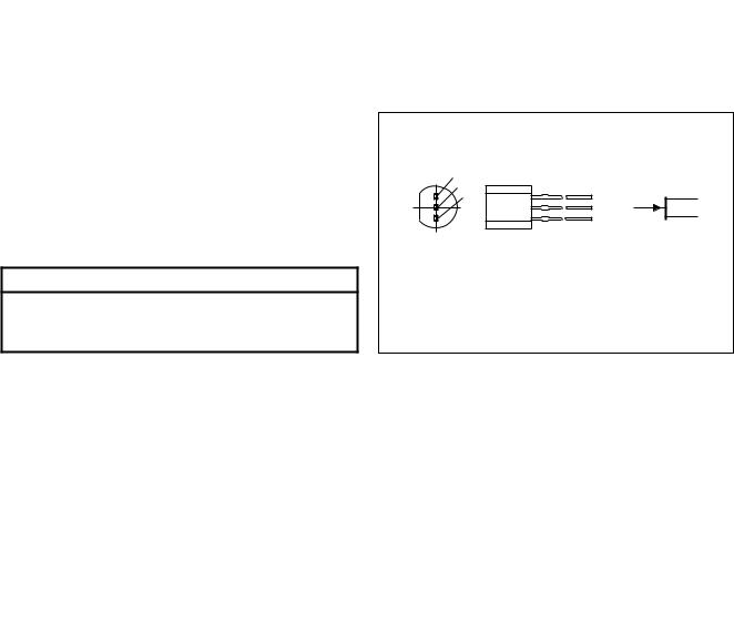
1
handbook, halfpage2 |
|
3 |
d |
|
g |
|
s |
|
MAM197 |
Fig.1 Simplified outline and symbol.
SYMBOL |
PARAMETER |
CONDITIONS |
MIN. |
MAX. |
UNIT |
|
|
|
|
|
|
VDS |
drain-source voltage |
|
− |
±25 |
V |
VGSoff |
gate-source cut-off voltage |
ID = 1 μA; VDS = 5 V |
|
|
|
|
J108 |
|
−3 |
−10 |
V |
|
J109 |
|
−2 |
−6 |
V |
|
J110 |
|
−0.5 |
−4 |
V |
|
|
|
|
|
|
IDSS |
drain current |
VGS = 0; VDS = 5 V |
|
|
|
|
J108 |
|
80 |
− |
mA |
|
J109 |
|
40 |
− |
mA |
|
J110 |
|
10 |
− |
mA |
|
|
|
|
|
|
Ptot |
total power dissipation |
up to Tamb = 50 °C |
− |
400 |
mW |
1996 Jul 30 |
2 |

Philips Semiconductors |
|
|
Product specification |
||||
|
|
|
|
|
|
|
|
N-channel silicon junction FETs |
|
J108; J109; J110 |
|||||
|
|
|
|
|
|
|
|
LIMITING VALUES |
|
|
|
|
|
|
|
In accordance with the Absolute Maximum Rating System (IEC 134). |
|
|
|
|
|
||
|
|
|
|
|
|
|
|
SYMBOL |
PARAMETER |
CONDITIONS |
MIN. |
|
MAX. |
UNIT |
|
|
|
|
|
|
|
|
|
VDS |
drain-source voltage |
|
− |
|
±25 |
|
V |
VGSO |
gate-source voltage |
open drain |
− |
|
−25 |
V |
|
VGDO |
gate-drain voltage |
open source |
− |
|
−25 |
V |
|
IG |
forward gate current (DC) |
|
− |
|
50 |
|
mA |
Ptot |
total power dissipation |
up to Tamb = 50 °C |
− |
|
400 |
|
mW |
Tstg |
storage temperature |
|
−65 |
|
150 |
|
°C |
Tj |
operating junction temperature |
|
− |
|
150 |
|
°C |
THERMAL CHARACTERISTICS |
|
|
|
|
|
|
|
|
|
|
|
|
|||
SYMBOL |
PARAMETER |
VALUE |
|
UNIT |
|||
|
|
|
|
|
|
|
|
Rth j-a |
thermal resistance from junction to ambient |
250 |
|
|
|
K/W |
|
STATIC CHARACTERISTICS
Tj = 25 °C; unless otherwise specified.
SYMBOL |
PARAMETER |
CONDITIONS |
MIN. |
TYP. |
MAX. |
UNIT |
|
|
|
|
|
|
|
V(BR)GSS |
gate-source breakdown voltage |
IG = −1 μA; VDS = 0 |
− |
− |
−25 |
V |
VGSoff |
gate-source cut-off voltage |
ID = 1 μA; VDS = 5 V |
|
|
|
V |
|
J108 |
|
−3 |
− |
−10 |
V |
|
J109 |
|
−2 |
− |
−6 |
V |
|
J110 |
|
−0.5 |
− |
−4 |
V |
|
|
|
|
|
|
|
IDSS |
drain current |
VGS = 0; VDS = 15 V |
|
|
|
|
|
J108 |
|
80 |
− |
− |
mA |
|
J109 |
|
40 |
− |
− |
mA |
|
J110 |
|
10 |
− |
− |
mA |
|
|
|
|
|
|
|
IGSS |
gate leakage current |
VGS = −15 V; VDS = 0 |
− |
− |
−3 |
nA |
IDSX |
drain-source cut-off current |
VGS = −10 V; VDS = 5 V |
− |
− |
3 |
nA |
RDSon |
drain-source on-state resistance |
VGS = 0; VDS = 100 mV |
|
|
|
|
|
J108 |
|
− |
− |
8 |
Ω |
|
J109 |
|
− |
− |
12 |
Ω |
|
J110 |
|
− |
− |
18 |
Ω |
|
|
|
|
|
|
|
1996 Jul 30 |
3 |
 Loading...