


PDM41257LA10SOA
PARADIGM PDM41257LA10SOA, PDM41257LA10SOATR, PDM41257LA10SOATY, PDM41257LA10SOI, PDM41257LA10SOITR Datasheet
...
Rev. 2.2 - 4/27/98 1
1
2
3
4
5
6
7
8
9
10
11
12
Features
n
High-speed access times
Com’l: 7, 8, 10, 12 and 15 ns
Industrial: 8, 10, 12 and 15 ns
n
Low power operation (typical)
- PDM41257SA
Active: 400 mW
Standby: 150 mW
- PDM41257LA
Active: 350 mW
Standby: 25 mW
n
Single +5V (
±
10%) power supply
n
TTL compatible inputs and outputs
n
Packages
Plastic SOJ (300 mil) - SO
Description
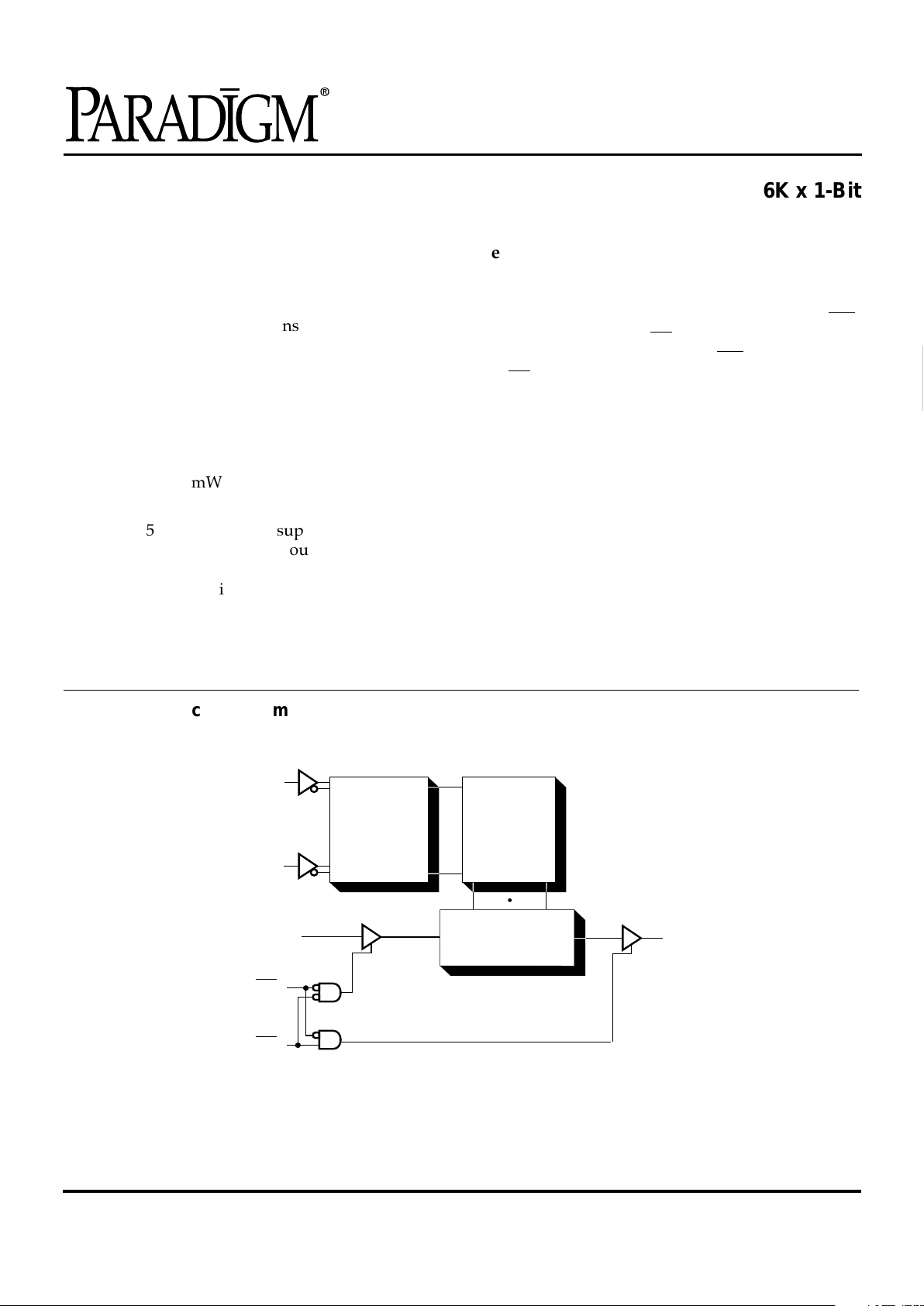
The PDM41257 is a high-performance CMOS static
RAM organized as 262,144 x 1 bit. Writing to this
device is accomplished when the write enable (WE
)
and the chip enable (CE
) inputs are both LOW.
Reading is accomplished when WE
remains HIGH
and CE
goes LOW.
The PDM41257 operates from a single +5V power
supply and all the inputs and outputs are fully TTL-
compatible. The PDM41257 comes in two versions,
the standard power version PDM41257SA and a low
power version the PDM41257LA. The two versions
are functionally the same and only differ in their
power consumption.
The PDM41257 is available in a 24-pin 300-mil
plastic SOJ for surface mount applications.
A0
•
•
•
•
•
A17
•
•
•
•
•
CE
WE
Addresses
Decoder
Memory
Matrix
Column I/O
•••••
D
IN
D
OUT
Functional Block Diagram
PDM41257
256K Static RAM
256K x 1-Bit
PDM41257
2 Rev. 2.2 - 4/27/98
T ruth T able
NOTE: 1. H = V
IH
, L = V
IL
, X = DON’T CARE
Absolute Maximum Ratings
(1)
NOTE: 1. Stresses greater than those listed under ABSOLUTE MAXIMUM RATINGS may
cause permanent damage to the device. This is a stress rating only and functional
operation of the device at these or any other conditions above those indicated in the
operational sections of this specification is not implied. Exposure to absolute maxi-
mum rating conditions for extended periods may affect reliability.
2. Appropriate thermal calculations should be performed in all cases and specifically for
those where the chosen package has a large thermal resistance (e.g., TSOP). The
calculation should be of the form
: T
j
= T
a
+ P *
θ
ja
, where T
a
is the ambient tempera-
ture, P is average oper ating po w er and
θ
ja
the thermal resistance of the package. For
this product, use the following
θ
ja
value:
SOJ: 83
o
C/W
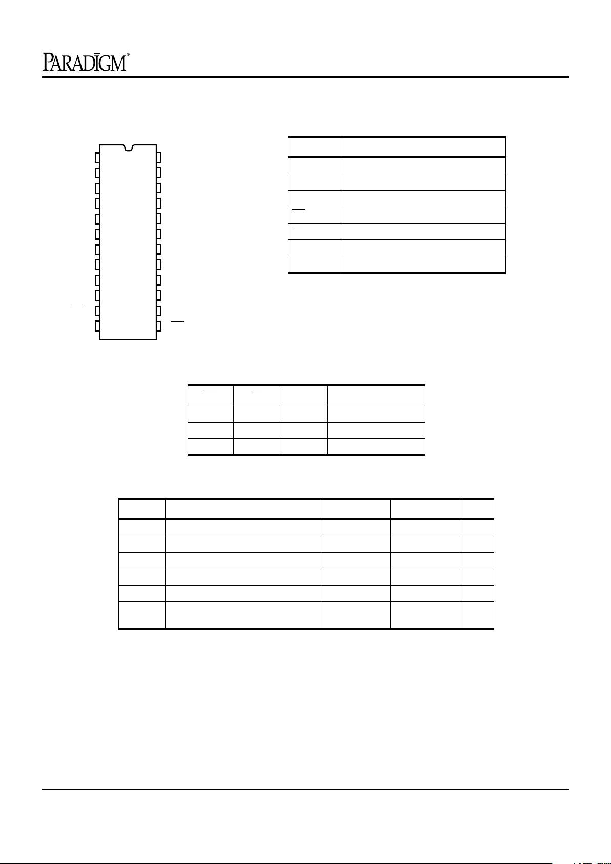
WE CE D
OUT
MODE
X H Hi-Z Standby
HLD
OUT
Read
L L Hi-Z Write
Symbol Rating Com’l. Ind. Unit
T
TERM
Terminal Voltage with Respect to V
SS
–0.5 to +7.0 –0.5 to +7.0
°
C
T
BIAS
Temperature Under Bias –55 to +125 –65 to +135
°
C
T
STG
Storage Temperature –55 to +125 –65 to +150
°
C
P
T
Power Dissipation 1.0 1.0 W
I
OUT
DC Output Current 50 50 mA
T
j
Maximum Junction Temperature
(2)
125 145
°
C
SOJ
1
2
3
4
5
6
7
8
9
10
11
12 13
14
15
16
17
18
19
20
21
22
23
24
A0
A1
A2
A3
A4
A5
A6
A7
A8
D
OUT
WE
Vss
Vcc
A17
A16
A15
A14
A13
A12
A11
A10
A9
D
IN
CE
Pin Configuration
Pin Description
Name Description
A17-A0 Address Inputs
D
IN
Data Input
D
OUT
Data Output
WE
Write Enable Input
CE
Chip Enable Input
V
CC
Power (+5V)
V
SS
Ground
PDM41257
Rev. 2.2 - 4/27/98 3
1
2
3
4
5
6
7
8
9
10
11
12
Recommended DC Operating Conditions
DC Electrical Characteristics
(V
CC
= 5.0V
±
10%)
NOTE: 1. V
IL
(min) = –3.0V for pulse width less than 20 ns.
Power Supply Characteristics
SHADED AREA = PRELIMINARY DATA
NOTE: All values are maximum guaranteed values.
Symbol Parameter Min. Typ. Max. Unit
V
CC
Supply Voltage 4.5 5.0 5.5 V
V
SS
Supply Voltage 0 0 0 V
Commercial Ambient T emperature 0 25 70
°
C
Industrial Ambient T emperature –40 25 85
°
C
PDM41257SA PDM41257LA
Symbol Parameter Test Conditions Min. Max. Min. Max. Unit
I
LI
Input Leakage Current V
CC
= MAX., V
IN
= V
SS
to V
CC
Com’l/
Ind.
–55–55
µ
A
I
LO
Output Leakage Current V
CC
= MAX.,
CE
= V
IH
, V
OUT
= V
SS
to V
CC
Com’l/
Ind.
–55–55
µ
A
V
IL
Input Low Voltage –0.5
(1)
0.8 –0.5
(1)
0.8 V
V
IH
Input High Voltage 2.2 6.0 2.2 6.0 V
V
OL
Output Low Voltage I
OL
= 8 mA, V
CC
= Min.
I
OL
= 10 mA, V
CC
= Min.
—
—
0.4
0.5
—
—
0.4
0.5
V
V
V
OH
Output High Voltage I
OH
= –4 mA, V
CC
= Min. 2.4 — 2.4 — V
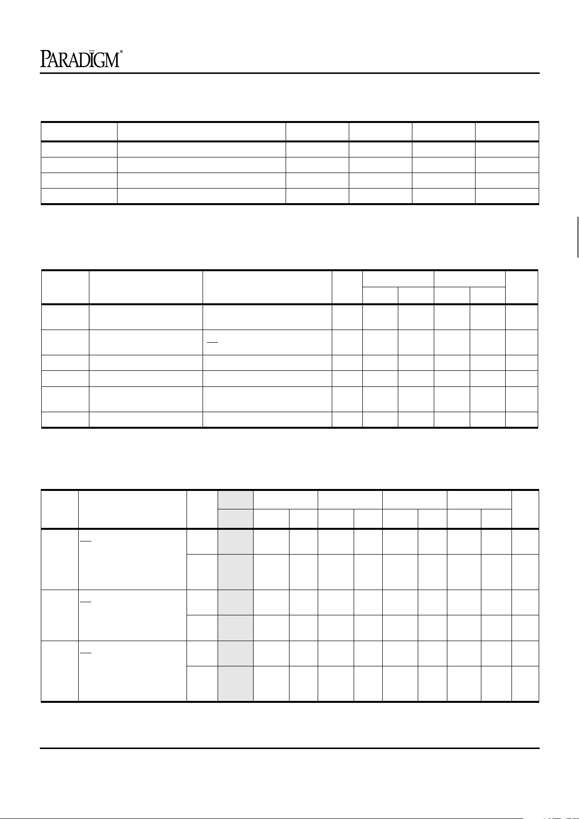
-7 -8 -10 -12 -15
Symbol Parameter Power
Com’l. Com’l. Ind. Com’l. Ind. Com’l. Ind. Com’l. Ind. Units
I
CC
Operating Current
CE
= V
IL
SA 210 200 210 190 200 180 190 170 180 mA
f = f
MAX
= 1/t
RC
V
CC
= Max
I
OUT
= 0 mA
LA
190 180 190 170 180 160 170 150 160 mA
I
SB
Standby Current
CE
= V
IH
SA
90 80 80 70 70 60 60 50 50 mA
f = f
MAX
= 1/t
RC
V
CC
= Max
LA
90 80 80 70 70 60 60 50 50 mA
I
SB1
Full Standby Current
CE
≥
V
CC
– 0.2V
SA
20 20 20 20 20 20 20 20 20 mA
f = 0
V
CC
= Max
V
IN
≥
V
CC
– 0.2V or
≤
0.2V
LA
5 55555555mA
 Loading...