


PANJIT TSP160B, TSP140B, TSP220B, TSP190B, TSP065B Datasheet
...PRELIMINARY


 TSP058B - TSP320B
AXIAL LEAD BI-DIRECTIONAL THYRISTOR SURGE PROTECTOR DEVICE
FEATURES
•Protects by limiting voltages and shunting surge currents away from sensitive circuits
•Designed for telecommunications applications such as line cards, modems, PBX, FAX, LAN,VHDSL
•Helps meet standards such as GR1089, ITU K.20, IEC950, UL1459&50, FCC part 68
•Low capacitance, High surge (A, B, C rating available), precise voltage limiting, Long life
|
|
|
|
|
|
|
|
|
|
|
DO-15 |
|||
SUMMARY ELECTRICAL CHARACTERISTICS |
|
|
|
|
|
|
|
|
|
|
||||
|
|
|
|
|
|
|
|
|
|
|||||
|
|
|
|
|
|
|
|
|
|
|
|
|
|
|
|
|
|
|
|
|
|
|
|
|
|
|
|
|
|
|
Rated Repetitive |
Breakover |
On-State |
Repetitive |
Breakover |
Holding |
Off-State Capacitance |
|||||||
|
PeakOff-State |
PeakOff-State |
||||||||||||
|
Voltage |
Voltage |
Voltage |
Current |
Current |
Currnet |
(f = 1 MHz, Vac = 15 mVRMS) |
|||||||
Part Number |
|
|
|
|
|
|
|
|
|
|
|
|
||
|
|
|
|
|
|
|
|
|
|
|
|
|
|
|
Max. |
Max. |
Max. |
Max. |
Max. |
Min. |
Typ. |
|
Max. |
Typ. |
|
Max. |
|||
|
|
|
||||||||||||
|
VDRM |
VBO @ IBO |
VT @ 1A |
I DRM |
I BO |
I H |
CO @ 0 Vdc |
CO @ 50 Vdc |
||||||
|
V |
V |
V |
µ A |
mA |
mA |
|
pF |
|
pF |
||||
TSP058B |
58 |
77 |
5 |
5 |
800 |
150 |
70 |
|
100 |
24 |
|
29 |
|
|
TSP065B |
65 |
88 |
5 |
5 |
800 |
150 |
67 |
|
90 |
22 |
|
28 |
|
|
|
|
|
|
|
|
|
|
|
|
|
|
|
|
|
TSP075B |
75 |
98 |
5 |
5 |
800 |
150 |
67 |
|
78 |
23 |
|
27 |
|
|
TSP090B |
90 |
130 |
5 |
5 |
800 |
150 |
57 |
|
61 |
19 |
|
21 |
|
|
|
|
|
|
|
|
|
|
|
|
|
|
|
|
|
TSP120B |
120 |
160 |
5 |
5 |
800 |
150 |
50 |
|
58 |
17 |
|
20 |
|
|
TSP140B |
140 |
180 |
5 |
5 |
800 |
150 |
49 |
|
54 |
16 |
|
19 |
|
|
|
|
|
|
|
|
|
|
|
|
|
|
|
|
|
TSP160B |
160 |
220 |
5 |
5 |
800 |
150 |
46 |
|
53 |
15 |
|
18 |
|
|
TSP190B |
190 |
260 |
5 |
5 |
800 |
150 |
45 |
|
53 |
14 |
|
18 |
|
|
|
|
|
|
|
|
|
|
|
|
|
|
|
|
|
TSP220B |
220 |
300 |
5 |
5 |
800 |
150 |
44 |
|
52 |
13 |
|
18 |
|
|
TSP275B |
275 |
350 |
5 |
5 |
800 |
150 |
44 |
|
51 |
13 |
|
18 |
|
|
|
|
|
|
|
|
|
|
|
|
|
|
|
|
|
TSP320B |
320 |
400 |
5 |
5 |
800 |
150 |
43 |
|
50 |
13 |
|
17 |
|
|
notes |
(1,3) |
(3,5,6) |
(3) |
(3) |
(3) |
(2,3) |
(3) |
|
(3) |
(3) |
|
(3) |
|
|
|
|
|
|
|
|
|
|
|
|
|
|
|
|
|
NOTES:
1.Specific VDRM values are available by request.
2.Specific IH values are available by request.
3.All ratings and characteristics are at 25 °C unless otherwise specified.
4.VDRM applies for the life of the device. IDRM will be in spec during and following operation of the device.
5.VBO1 is at 100V/msec, ISC =10Apk, VOC=1KVpk, 10/1000 Waveform
6.VBO2 is at f = 60 Hz, ISC = 1 A(RMS), Vac = 1KV(RMS), RL = 1 KΩ , 1/2 AC cycle
TSP058B - TSP320B THYRISTOR
Ver: June 2001 |
PAGE 1 |


 TSP058B - TSP320B
PRELIMINARY |
|
|
|
|
|
|
|
|
|
|
SELECTION GUIDE |
|
|
|
|
|
|
|
|
||
|
|
|
|
|
|
|
|
|
||
|
|
|
|
|
|
|
|
|
||
|
Follow these steps to select the proper Thyristor surge protector for your application: |
|
|
|||||||
|
1. Define the operating parameters for the circuit: |
|
|
|
|
|
||||
|
• Ambient operating temperature range |
|
|
|
|
|
|
|||
|
• Maximum telephone line operating current (highest battery and shortest copper loop) |
|
|
|||||||
|
• Maximum operating voltage: (Maximum DC bias + peak ringing voltage) |
|
|
|
||||||
|
• Maximum surge current |
|
|
|
|
|
|
|
|
|
|
• System voltage damage threshold |
|
|
|
|
|
|
|||
|
• Select device with an off-state voltage rating (VDRM) above the maximum operating voltage at the minimum operating temperature. |
|||||||||
|
3. Select surge current ratings (IPPS and ITSM) ≥ those which the application must withstand. |
|
|
|||||||
|
4. Verify that the minimum holding current of the device at the maximum ambient temperature is above the maximum dc current of the |
|||||||||
|
system. |
|
|
|
|
|
|
|
|
|
|
5. Verify that the maximum breakover voltage of the device is below the system damage threshold. |
|
||||||||
|
6. Verify that the circuit's ambient operating temperatures are within the device's operating temperature range. |
|||||||||
|
7. Verify that the device's dimensions fit the application's space considerations. |
|
|
|||||||
|
8. Independently evaluate and test the suitability and performance of the device in the application |
|
||||||||
|
MAXIMUM SURGE RATINGS (TJ = 25 ºC UNLESS OTHERWISE NOTED) |
|||||||||
|
|
|
|
|
|
|
|
|
|
|
|
|
|
|
|
|
|
|
|
|
|
|
Rating |
|
|
|
Non-Repetitive Peak Pulse Current |
|
Non-Repetitive Peak |
|||
|
|
|
|
|
On-State Surge Current |
|||||
|
|
|
|
|
|
|
|
|
|
|
|
Symbol |
|
|
|
|
|
I PPS |
|
|
I TSM |
|
Short-Circuit Current Wave |
|
2/10 s |
|
8/20 s |
10/160 s |
5/310 s |
10/560 s |
10/1000 s |
|
|
|
|
|
|
|
|
|
|
|
30A |
|
Open-Circuit Voltage Wave |
|
2/10 s |
|
1.2/50 s |
10/160 s |
10/700 s |
10/560 s |
10/1000 s |
|
|
Value |
|
300 A |
|
225 A |
150 A |
115 A |
100 A |
80 A |
|
|
Notes |
|
|
|
|
(1,2,4,5,6) |
|
|
(1,2,3,4) |
|
|
|
|
|
|
|
|
|
|
|
|
Notes:
1.Thermal accumulation between successive surge tests is not allowed.
2.The device under test initially must be in thermal equilibrium with TJ = 25 °C.
3.Test at 1 cycle, 60 Hz.
4.Surge ratings are non-repetitive because instantaneous junction temperatures may exceed the maximum rated TJ. Nevertheless, devices will survive many surge applications without degradation. Surge capability will not degrade over a device's typical operating life.
5.Adjust the surge generator for optimum current-wave
accuracy when both voltage and current wave specifications cannot be exactly met. The current wave is more important than the voltage wave for accurate surge evaluation.
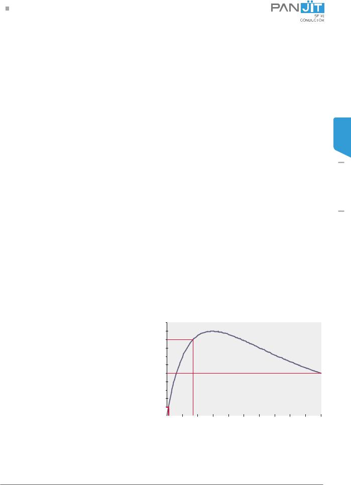
6.The waveform is defined as A/B ms where:
A:(Virtual front time) = 1.25 X Rise time = 1.25 X (Tb - Ta)
B (Duration time to 50% level of Ipps) = T1 - T0
% Ipps
100%
80%
60%
40%
20%
0% |
|
|
|
|
|
|
|
|
|
|
|
|
|
To Ta |
Tb |
Time |
T1 |
|||
|
|
|
|
|
|
|
TSP058B - TSP320B THYRISTOR
Ver: June 2001 |
PAGE 2 |

PRELIMINARY


 TSP058B - TSP320B
MAXIMUM THERMAL RATINGS
Rating |
Symbol |
Value |
Unit |
|
|||
|
|
|
|
Storage Junction Temperature Range |
TSTG |
-50 to 150 |
OC |
Operating Junction Temperature Range |
TJ |
-40 to 150 |
OC |
Operating Ambient Temperature Range |
Ta |
-40 to 65 |
OC |
Notes:
PCB board mounted on minimum foot print.
|
|
|
|
|
THYRISTOR |
THERMAL CHARACTERISTICS |
|
|
|
|
|
|
|
|
|
TSP320B |
|
|
|
|
|
|
|
|
|
|
|
|
|
Characteristic |
Symbol |
Value |
Unit |
|
|
|
|
|
|
|
- |
Thermal Resistance Junction to Leads TL on tab adjacent to |
Rθ JL |
Max. 20 |
OC / W |
|
TSP058B |
plastic. Both leads soldered to identical pad sizes. |
|
|
|||
|
|
|
|
|
|
|
|
|
|
|
|
Notes:
The junction to lead thermal resistance represents a minimum limiting value with both leads soldered to a large near-infinite heatsink. The junction to ambient thermal resistance depends strongly on board mounting conditions and typically is 3 to 6 times higher than the junction to lead resistance. The data shown is to be used as guideline values for preliminary engineering.
ELECTRICAL CHARACTERISTICS (TC = 25°C UNLESS OTHERWISE NOTED)
Parameters
Repetitive Peak
Off-State Current
Breakover Current
Holding Current1
On-State Voltage
Test Conditions |
Symbol |
Min. |
Max. |
Unit |
VD = rated VDRM |
I DRM |
|
5 |
µ A |
|
|
|
|
|
f = 60 Hz, ISC = 1 Arms, Vac = 1 KVrms, RL = 1 KΩ , 1/2 AC cycle |
I BO |
|
800 |
mA |
10/1000µ s waveform, ISC = 10A, VOC = 62 V, RL = 400 Ω |
I H |
150 |
|
mA |
|
|
|
|
|
I T = 1 A, Tw = 300 µ s, 1 pulse |
VT |
|
5 |
V |
|
|
|
|
|
Notes:
Specific IH values are available by request.
Ver: June 2001 |
PAGE 3 |
 Loading...