


TX-32LE60F
Table of contents
 Loading...
ORDER No. PCZ0608063CE
Service Manual
Colour LCD Television
TX-32LE60F
TX-32LE60P
TX-26LE60F
TX-26LE60P
GLP21 Chassis
Specifications
(Informations in brackets [ ] refers to models 26´´)
Power Source: 220-240V AC
Power Consumption: 117W [104W]
Stand-by Power
Cons
umption: 1W [1W]
Aerial Impedance: 75Ω unbalanced,
Receiving System: PAL-B/G
Receiving Channels:
VHF E2-E12 VHF H1-H2 (ITALY)
VHF A-H (ITALY) VHF R1-R2
VHF R3-R5 VHF R6-R12
UHF E21-E69 CATV (S01-S05)
CATV S1-S10 (M1-M10) CATV S11-S20 (U1-U10)
CATV S21-S41 (Hyperband)
Operating Conditions:
Temperature: 5°C ÷ 35
Humidity: 5% ÷ 90
Intermediate Frequency:
Video/Audio
Video
Audio 33,4MHz (B/G), 33,16MHz (A2)
Colour 34,47MHz (PAL)
Terminals:
AV1 IN Video (21 pin) 1V p-p 75Ω
AV1 OUT Video (21 pin) 1V p-p 75Ω
SECAM B/G, D/K, L/L’
PAL-525/60 (AV only)
M.NTSC (AV only)
NTSC (AV o
38,9MHz, 33,9MHz
33,05MHz (NICAM B/G, D/K, L)
32,4MHz (D/K), 32,66MHz (CZ STEREO)
40,4MHz (L’), 39,75Mhz (L’NICAM),
34,5MHz, 34,65MHz (SECAM)
38,3MHz, 38,15MHz (SECAM L’)
Audio (21 pin) 500mV rms 10kΩ
RGB (21 pin) 0,7V p-p 75Ω
Audio (21 pin) 500mV rms 1kΩ
, 50Hz
Coaxial Type
, D/K,
nly)
°C
% RH (non-condensing)
AV2 IN Video (21 pin) 1V p-p 75Ω
AV2 OUT Video (21 pin) 1V p-p 75Ω
AV3 IN S-Video IN Y: 1V p-p 75Ω
HDMI1 Type A Connector
COMPONENT YUV Video (RCAx3) Y:1V p-p 75Ω
AUDIO IN Audio (RCAx2) 500mV rms 10kΩ
LCD screen: L5EDD8
Audio Output: 2x10W RMS
Headphones: 3,5mm, 8Ω Imp
Accessories
supplied : Remote Con
Dimensions:
Including TV stand 615mm 791mm 301mm
TV set only 563mm 791mm 107mm
Net weight: 17,5kg
Specifications are subject to change w
Weights and dimensions shown are approximate.
Audio (21 pin) 500mV rms 10kΩ
RGB (21 pin) 0,7V p-p 75Ω
S-video IN Y: 1V p-p 75Ω
(21-pin) C:0,3V p-p 75Ω
Audio (21 pin) 500mV rms 1kΩ
(4-pin) C:0,3V p-p 75Ω
Audio (RCAx2) 500mV rms 10kΩ
Video (RCAx1) 1V p-p 75Ω
Pb, Pr: 0,7V p-p 75Ω
Q00023 [L5EDD6Q00017]
1366 x 768 XGA, 16:9
Visible Diagonal 800mm [660mm]
8Ω impedance
edance
trol
2 x R6 (UM3) Batteries
Height: Width: Depth:
[525mm] [657mm] [301mm]
[473mm] [657mm] [107mm]
[14,kg]
ithout notice.

CONTENTS
SAFETY PRECAUTIONS........................................... 3
GENERAL GUIDE LINES...................................... 3
TOUCH – CURRENT CHECK
PREVENTION OF ELECTROSTATIC DISCHARGE
(ESD) TO ELEC
DEVICES.................................................................... 4
ABOUT LEAD FREE SOLDER (PBF)
SUGGESTED PB FREE SOLDER
SERVICE HINT
CHASSIS BOARD LAYOUT
SETTING INSPECTION.............................................. 7
SELF-CHECK
ADJUSTMENT ME
BLOCK DIAGRAMS
TROSTATICALLY SENSITIVE (ES)
S ........................................................ 6
............................................................. 8
THOD ........................................... 9
.................................................. 10
............................... 3
......................... 5
........................ 5
....................................... 7
PARTS LOCATION................................................... 13
REPLACEMENT PARTS LIST.................................. 14
SCHEMATIC DIAGRAMS.........................................
A-BOARD (1 OF 5) SCHEMATIC DIAGRAM......26
A-BOARD (2 OF 5) SCHEMATIC DIAGRAM......27
A-BOARD (3 OF 5) SCHEMATIC DIAGRAM......28
A-BOARD (4 OF 5) SCHEMATIC DIAGRAM......29
A-BOARD (5 OF 5) SCHEMATIC DIAGRAM......30
P-BOARD SCHEMATIC DIAGRAM
B-BOARD SCHEMATIC DIAGRAM
H-BOARD SCHEMATIC DIAGRAM
V-BOARD SCHEMATIC DIAGRAM
K-BOARD SCHEMATIC DIAGRAM
CONDUCTOR VIEWS
.............................................. 34
.................... 31
.................... 32
.................... 32
.................... 33
.................... 33
25
2

Safety Precautions
A
Ω
Ω
Ω
Ω
General Guide Lines
1. When servicing, observe the original lead dress. If a short circuit is found, replace all parts which have been overheated
or damaged by the short circuit.
2. After servicing, see to it that all the protective devices such as insulation barriers, insulation papers shields are properly
installed.
3. After servicing, make the following touch current checks to prevent the customer from being exposed to shock hazards.
4. Always ensure panel TKKL5290 is correctly replaced before returning to customer (see Fig.1).
Fig. 1
Touch-Current Check
1. Plug the AC cord directly into the AC outlet. Do not use an isolation transformer for this check.
2. Connect a measuring network for touch currents between each exposed metallic part on the set and a go od earth
ground such as a water pipe, as shown in Fig. 2.
3. Use Leakage Current Tester (Simpson 228 or equivalent) to measure the potential across the measuring network.
4. Check each exposed metallic part, and measure the voltage at each point.
5. Reserve the AC plug in the AC outlet and repeat each of the above measure.
6. The potential at any point (TOUCH CURRENT) expressed as voltage U1 and U2, does not exceed the following values:
For a. c.: U1 = 35 V (peak) and U2 = 0.35 V (peak);
For d. c.: U1 = 1.0 V,
Note:
The limit value of U2 = 0.35 V (peak) for a. c. and U1 = 1.0 V for d. c. correspond to the values 0.7 mA (peak) a. c. and
2.0 mA d. c.
The limit value U1 = 35 V (peak) for a. c. correspond to the value 70 mA (peak) a. c. for frequencies greater than 100
kHz.
7. In case a measurement is out of the limits specified, there is a possibility of a shock hazard, and the equipment should
be repaired and rechecked before it is returned to the customer.
Measuring network for TOUCH CURRENTS
COLD
WATER PIPE
(EARTH GROUND)
Fig. 2
CS=0.22µF
10k
U
1
0.022µF
V
U2 (V)
RS=1500
TO
PPLIANCES
EXPOSED
METAL PARTS
Resistance values in ohms (Ω)
V: Voltmetr or oscilloscope
(r.m.s. or peak reading)
NOTE – Appropriate measures should be taken to obtain the correct value in case of non-sinusoidal waveforms
Input resistance: ≥ 1M
Input capacitance: ≤ 200pF
Frequency range: 15Hz to 1MHz and d.c.respectively
R0=500
3

Prevention of Electrostatic Discharge (ESD) to Electrostatically
Sensitive (ES) Devices
Some semiconductor (solid state) devices can be damaged easily by static electricity. Such components commonly are
called Electrostatically Sensitive (ES) Devices. Examples of typical ES devices are integrated circuits and some field-effect
transistors and semiconductor "chip" components. The following techniques should be used to help reduce the incidence of
component damage caused by electrostatic discharge (ESD).
1. Immediately before handling any semiconductor component or semiconductor-equipped assembly, drain off any ESD on
your body by touching a known earth ground. Alternatively, obtain and wear a commerciall y av ailable discharging ESD
wrist strap, which should be removed for potential shock reasons prior to applying power to the unit under test.
2. After removing an electrical assembly equipped with ES devices, place the assembly on a conductive surface such as
aluminum foil, to prevent electrostatic charge build up or exposure of the assembly.
3. Use only a grounded-tip soldering iron to solder or unsolder ES devices.
4. Use only an anti-static solder removal device. Some solder removal devices not classified as "anti-static (ESD
protected)" can generate electrical charge sufficient to damage ES devices.
5. Do not use freon-propelled chemicals. These can generate electrical charges sufficient to damage ES devices.
6. Do not remove a replacement ES device from its protective package until immediately before you are ready to install it.
(Most replacement ES devices are packaged with leads electrically shorted together by conductive foam, aluminum foil
or comparable conductive material).
7. Immediately before removing the protective material from the leads of a replacement ES device, touch the protective
material to the chassis or circuit assembly into which the device will be installed.
Caution
Be sure no power is applied to the chassis or circuit, and observe all other safety precautions.
8. Minimize bodily motions when handling unpackaged replacement ES devices. (Otherwise harmless motion such as the
brushing together of your clothes fabric or the lifting of your foot from a carpeted floor can generate static electricity
(ESD) sufficient to damage an ES device).
IMPORTANT SAFETY NOTICE
There are special components used in this equipment which are important for safety.
These parts are marked by in schematic diagrams, exploded views and replacement parts list. It is essential that
these critical parts should be replaced with manufacturer’s specified parts to prevent shock, fire, or other hazards. Do
not modify the original design without permission of manufacturer.
4
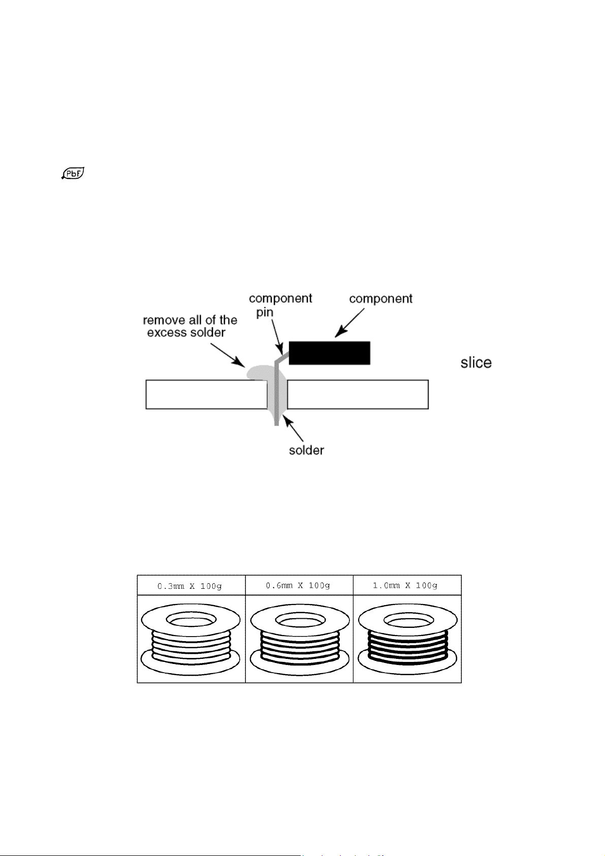
About lead free solder (PbF)
Note: Lead is listed as (Pb) in the periodic table of elements.
In the information below, Pb will refer to Lead s
The Lead Free Solder used in our manufacturing process and discussed below is (Sn+Ag+Cu).
That is Tin (Sn), Silver (Ag) and Copper (Cu) although other types are available.
This model uses Pb Free solder in it’s manufacture due to environmental conservation issues. For service and repair work,
we’d suggest the use of Pb free solder as well, although Pb solder may be used.
PCBs manufactured using lead free solder will have the PbF within a leaf Symbol
stamped on the back of PCB.
Caution
• Pb free solder has a higher melting point than standard solder. Typically the melting point is 50 ~ 70 °F (30~40°C)
higher. Please use a high temperature soldering iron and set it to 700 ± 20 °F (370 ± 10 °C).
• Pb free solder will tend to splash when heated too high (about 1100 °F or 600 °C).
If you must use Pb solder, please completely remove all of the Pb free so
applying Pb solder. If this is not practical, be sure to heat the Pb free solder until it melts, before applying Pb solder.
• After applying PbF solder to double layered boards, please check the component side for excess solder which may
flow onto the opposite side. (see Fig.3)
older, and PbF will refer to Lead Free Solder.
lder on the pins or solder area before
Fig.3
Suggested Pb free solder
There are several kinds of Pb free solder available for purchase. T
However, Sn+Cu (tin, copper), Sn+Zn+Bi (tin, zinc, bismuth) solder can also be used. (see Fig.4)
his product uses Sn+Ag+Cu (tin, silver, copper) solder.
Fig.4
5

Service Hints
How to remove the Pedestal assembly
Lay the main unit face down. (see Fig.5)
Fig.5
Remove the 2 fixing screws and hinge cover. (see Fig.6)
Remove the 8 fixing screws and the pedestal assembly. (see Fig.7)
SCREWS
Fig.6
How to remove the backcover
Remove the 2 fixing screws and hinge cover. (see Fig.6)
Remove the 16 fixing screws. (see Fig.8)
Carefully remove the backcover and disconnect two AV3 wires. (see Fig.9)
SCREWS
Fig.7
SCREWS
Fig.8
Fig.9
6
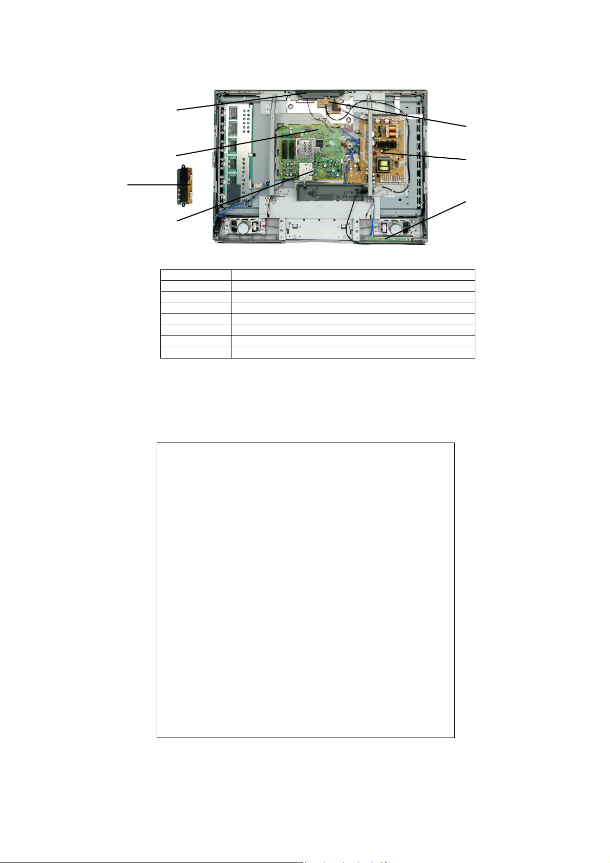
Chassis Board Layout
A
KEY CONTROL
K-BOARD
-BOARD
H-BOARD
B-BOARD
Board Name Function
A-Board Main Board
B-Board Tuner
H-Board AV3 Terminal
Key Control Key Control
K-Board Mains Input, Power Switch
P-Board Power Supply
V-Board Remote Receiver, LED IR, Bats
Setting Inspection
Voltage Confirmation
A board Normal mode
Test point Position Voltage
TP004 C870, + pin
TP005 Connector A7, pin 22 12V [15V]
TP006 C1500, + pin
TP008 C1700, + pin
TP010 C890 - R898
TP012 Q878, pin 1
TP017 Connector A7, pin16
TP018 IC252, pin 5 24V
TP019 IC862, pin 1 24V
TP023 Connector A7, pin 12 24V
P-BOARD
V-BOARD
Confirm the following voltages:
33V ± 3V
8V ± 0,3V
5V ± 0,2V
3,3V ± 0,1V
3,3V ± 0,1V
10,5V ÷ 16V
Standby mode
TP009 C883, + pin
TP013 C868, + pin
P board
TP001 Connector P2, pin 20
TP002 Connector P2, pin 8
TP003 Connector P2, pin 9
TP002 Connector P2, pin 8 24V
TP003 Connector P2, pin 9
1,8V ± 0,1V
3,3V ± 0,1V
Normal mode
12V ± 2V [15V± 2V]
24V ± 2V
24V ± 1V
Standby mode
<2V
7
Self Check
A
Self-check is used to automatically check the bus lines and hexadecimal code of the TV set. To enter Self-Check mode, keep
pressing the STATUS button on the remote control and press the down (-/v) button on the TV set. To exit Self Check,
switch off the TV set at the power button.
E2 O.K.
DPS O.K.
VSP O.K.
VSW O.K.
TUN O.K.
MSP O.K.
DPL --MAS ---
TX-32LE60F TX-32LE60P TX-26L E60F TX-26LE60P
OPTION 1 0F 0F 0F 0F
OPTION 2 00 00 00 00
OPTION 3 B9 B9 B9 B9
OPTION 4 11 11 11 11
OPTION 5 00 00 00 00
OPTION 6 15 15 15 15
OPTION 7 FD FD FD FD
OPTION 8 D0 50 D0 50
OPTION 9 00 00 00 00
OPTION 10 20 20 20 20
OPTION 11 13 13 13 13
OPTION 12 20 20 20 20
OPTION 13 1C 1C 1C 1C
CHECK 2A AA 2A AA
Display Ref. No. Description P.C.B.
E2 IC1120 EAROM A-Board
DPS IC1501 DISPLAY PROCESSOR AND SCALER A-Board
VSP IC1501 VIDEOSIGNAL PROCESSOR A-Board
AVSW IC1501 AV SWITCH A-Board
TUN TNR001 TUNER B-Board
MSP IC1501 MULTISTANDART SOUND PROCESSOR A-Board
DPL --- DOLBY PROLOGIC PROCESSOR ---
MAS --- MPEG1 AUDIO PROCESSOR ---
If the CCU ports have been checked and found to be incorrect or not located then " - - " will appear in place of "O.K.".
8
Adjustment Method
How to enter Service 1
• Set the Bass to maximum position, set the Treble to minimum position then keep pressing the INDEX button on the
remote control and press the down button (-/v) on the TV set, this will place the TV set into the Service Mode 1.
Key Command
• Press the RED / GREEN buttons to step up / down through the functions.
• Press the YELLOW / BLUE buttons to alter the function values, to alter White Rasters use +/- buttons
• Press the OK button after each adjustment has been made to store the required values.
• To exit the Service Mode, press the "N" button.
Keep adjusting sequence: DVCO, Sub-Contrast, other items.
Item
Sub-Contrast
DVCO
Highlight
Lowlight
Sub-Brightness
Note: All setting values are approximate
High 12 0296 0300 0296
Low 4 0026 0054 0040
Setting indication
Sub-Contrast
23
DVCO
4
Sub-Brightness
0
Settings / Special features
Receive a 80% white level Philips Pattern with correct
sound sy
Contrast alignment press "Blue" button, wait until the
figure colour is changed from red to black colour.
Receive a 80% white level Philips Pattern via aerial
inp
until the figure colour is changed from red to black
For correct setting see W
stem (B/G, D/K) via aerial input. For Sub-
Press the OK.
ut. For DVCO alignment press "Blue" button, wait
colour. Press the OK.
hite Balance Adjustment
Optimum setting.
White Balance Adjustment
Instrument
• Remote Control
• LCD WB meter (Minolta CA-210 or equivalent)
Condition
• Switch on the TV Set. Enter Service1. Step down to Highlight line and keep the aging time more than 20 minutes.
Procedure
• After aging time above set White Raster No.12 for Highlight and No.4 for Lowlight Press the OK button
to store.
• Put Minolta Sensor to the center of the LCD Panel with 25mm gap between Minolta Sensor and LCD Panel. Adjust "x"
and "y" values by changing Red and Blue values.
• Press OK button to store setting.
Item Value
x
Highlight
Lowlight
0,280±0,002
y
0,285±0,002
x
0,275±0,002
y
0,285±0,002
High 12
Low 4
9

V
A5
L
L +
4
L -
16
13
AMP
IC251
4
SP L
28
321
R +
16
IC252
4
SP R
27
L
R
R
C
Y
R
L
H-BOARD
4
8
R -
13
AMP
JK3001
V
PR IN
PB IN
174
U
172
Y
Y IN
173
TO LCD PANEL
2
4
A2
TX0-
TX0+
TX1-
141
140
6
138
8
10
121814
16
20
TX1+
TX2-
137
135
TX3-
TX2+
TCLK-
TCLK+
TX3+
134
132
131
129
128
H1
A12
8
AV3 R IN
13
1
6
6
AV3 L IN
14
3
4
1
3
AV3 Y IN
AV3 C IN
AV3 CVBS IN
184
187
188
H2
A6
1
3
1
3
HP RIGHT
HP LEFT
1
7
IC1501
VIDEO PROCESSOR
1901211
AV2 CVBS IN
CVBS OUT 19
CVBS IN 20
R IN/C IN 15
G IN 11
B IN 7
L IN 6
R IN 2
L OUT 3
R OUT 1
AV2 21 PIN SCART
CVBS OUT 19
CVBS IN 20
R IN 15
AV1 21 PIN SCART
G IN 11
B IN 7
L IN 6
R IN 2
L OUT 3
R OUT 1
Video & Stereo Audio Block Diagram
178
177
176
109189
AV2 L IN
AV1 RED IN
AV1 GREEN IN
AV1 BLUE IN
AV1 LEFT IN
AV1 RIGHT IN
AV2 R IN
AV1 CVBS IN
AV2 L OUT
AV2 R OUT
181
179
180
IRD AV2 RED/C IN
IRD AV2 GREEN IN
IRD AV2 BLUE IN
15
IC3300
AUDIO MATRIX
IC270
HP AMPLIFIER
5
3
25
73-66
65-58
7
OP AMP
IC1381
2
11
123
D/A CONVERTER
I2SCL
MCLK
888684
1
6
10
I2SDI
26
4
I2SWS
85
R 8bit data bus
B 8bit data bus
G 8bit data bus
15
16
212324
22
194
195
AV1 CVBS OUT VCTP
AV2 CVBS OUT VCTP
Q3205
Q3204
Q3202
Q3201
HDMI DAC L
HDMI DAC R
AV2 L OUT VCTP
AV1 L OUT VCTP
AV1 R OUT VCTP
AV2 R OUT VCTP
AM IRD YUV/DVI R IN
AM IRD YUV/DVI L IN
6
5
4
25
24
16
17
14
23
191
SIFIN+
TUNER CVBS IN
Q123 Q122
SIF+
57-50
31
IC1380
12
13
18
11
AV1 L OUT
AV1 R OUT
YUV/DVI P0 R IN
YUV/DVI P0 L IN
10
AM
IC5003
HDMI RECEIVER
39,40,43,44,
TUNER CVBS IN
SIF+
AM
A-BOARD
L
R
A1
13
10
11
8Bit data
HDMI
132-129,126-123
119-116,113-110
144-140,137,136,133
47,48,51,52
JK3002
13
10
11
B1
AM 13
SIF_OUT 14
VIDEO OUT 17
TUNER
B-BOARD
10
,
,
,
,
,
,
,
C
3,3
,
,
,
,
,
,
K-BOARD
D5000
3
K3
SW 800
F800
1
K1
MAIN IN
1
4
LCF´S
3V
3V
13
P-BOARD
3V
3V
3V
LF802
LINE
FILTER
LF803
LINE
FILTER
IC801
MAIN PS CONTROL
8
101112
8
101112
IRD24V
SIGNAL24V
D877
4
REG
IC3884
5
23
11
15
10
7
19
20
16
SIGNAL24V
12V
12V
AUDIO24V
1,8
IC862
2
4
1
20-22
20-22
Q873
REG
L801
32
COMP
STB
VREF
VCC
D851
D852
D853
~
T801
2
REG
IC881
1
Q881
+
D801
-
10,11 [3,4]
14,15 [7,8]
16 [9]
AUD12_16
LCF´S
~
P3
24V
1-4
RL850
[17] 8
[13] 5
[10] 1
[14,15] 6
9 [2]
Q851
PC802
PC803
IC 850
REF
LCD PANEL
A2
26-30
PANEL 5V
PANEL 5V
Q1701
Q875
LCF
18-21
REG
IC885
11-14
LCF
6-7
REG
IC866
5
1
REG
IC3850
2
LCF
LCF
7
REG
IC5000
1
LCF´S
SUPDRI 3,3V
VSUPDIG 3,3V
VCC
RM1050
SUPCOM 3,3V
5V
5V MIXED P0
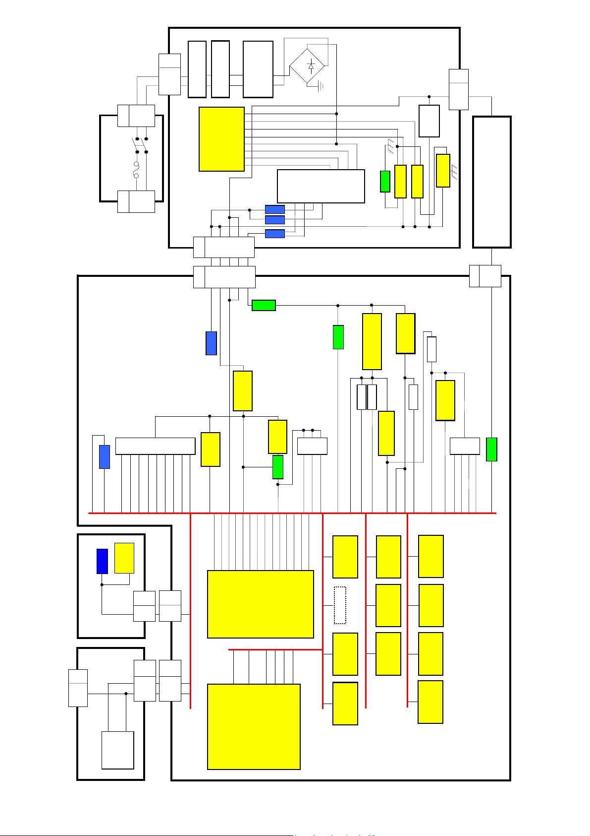
POWER SUPPLY BLOCK DIAGRAM
SN 1063
3,3V STBY
V-BOARD
B2
5V
1
SERVICE
33V
TUNER 5V
3
15
TUNER
B-BOARD
SUPFE 3
SUPVO 3
A8
6
A1
124
SUPLVDS 3
SUPDAC 3
CEC 3,8V
SUPSIF 5V
VSUPAU 8V
183336
STBY 3,3V
AUDIO 24V
3V
3V
SUPDRI 3
SUPDIG 3
45,75
8V
VSUPIO1 3,3V
SUPLVDS 1
VSUPLVDS 3,3V
77
114
124
96
86
IC1501
134
122
127,133,139,150,156
1V8 HD
3V3 PVCC
37,55
22,23,35,74,79,92,94,105,
114,128,139
VIDEO PROCESSOR
3V3 HD
IC5003
HDMI RECEIVER
5,6,7,13,16,19,26,76,89,109,
SUPIO3 3
SUPIO1 3,3V
V2
6
B1
124
STBY 1,8V
142
3V3 AVCC
38,42,46,50,57,61,65,69
V
PDA
VSUPFE 1,8V
185
164
169
3V3 XTAL
98
SUPDIG 1,8V
VSUPFE 3,3V
VSUPVO 3,3V
192
170
3V3 REG
99
A-BOARD
SUPLVDS 1,8V
3V
SUPIO3 3
197
SUPFE 1,8V
33V
5V
CEC 3,8V
5V MIXED P0
8V
14,9,8,7
HDMI_CEC
8
8
SUPSIF 5V
5V
DAC
IC1380
IC5001
EDID EPROM
OP AMP
IC1381
TUNER 5V
8V
8
AUDIO 24V
18,5
AUDIO 24V
18,5
HDMI 3,3V
8V 9V AUD SW
IC270
IC252
IC251
5V
3V3 REG
8V
VSUPAU 8V
3V3 HD
STBY 3,3VSTBY 3,3VSTBY 3,3V
16
HP AMP
AUDIO AMP
AUDIO AMP
IC1220
8
IC1120
2
IC1500
8V 9V AUD SW
3
IC3300
3V3 XTAL
3V3 AVCC
3V3 PVCC
1V8 HD
SWITCH
EAROM
RESET
AUD MATRIX
11

HDMI_AUDIO_MUTE
V
V
HDMI_HP_MUTE
HDMI_SMUTE_INHIBIT
AUDIO _MUTE
AMP Mute
UDIO
12-16V
Q1721
ENABLE 7
IC251
C1BB00000998
8
7
ENABLE
IC252
C1BB00000998
NOT_STBY
SDA3,3V
SCL3,3V
POWER
SUPPLY
Q877
HP Mute
BACKLIGHT_PWM
PWM_OUT
HDMI_HP_MUTE
33V
Q872
Q1101
SCL_TUNER
12V
SDA_TUNER
Q1100
3,3
Q879
LEVEL
SHIFTER
27
SCL
SDA 28
IC3300
TEA6422DT
DAC
IC1380
C0FBBK000047
13 AV1_SDA
15 AV1_SCL
6 HDMI_MUTE
5 HDMI_SMUTE_INHIBIT
Q1380
Q1223
16 FBL2
1 SCL3,3V
ANALOG
IC1220
74HC4053D
MULTIPLEXER
9 AV1_IS_QLINK
5 AV2_SCL
10,11 SERVICE
14 SDA3,3V
4 AV_LINK
Q1219
Q1232
Q1231Q1229
12 EEPROM_SDA
Q1222
Q1230
10 AV2_SCL
HDMI_SMUTE_INHIBIT
HDMI_MUTE
8 AV2 SLOW
AV1_IS_QLINK
SCL3,3V
AV_LINK_OUT
AV_LINK_IN
AV2_SCL
SERVICE
SDA3,3V
AV1_SCL
EEPROM_SDA
AV1_SDA
HDHS
STBY_LED
AUDIO_MUTE
BUS_REQUEST
AV1_IS_QLINK
AV_LINK_IN
AV_LINK_OUT
AV2_FBL
EDID_WP_DISABLE
SERVICE
AV1_FBL
Q1213
200
HDHS 171
AV2_FBL 183
STBY_LED 208
1 IR
AUDIO_MUTE 205
2 HDMI_5V_DET
BUS_REQUEST 204
3 PANEL ON
AV_LINK_IN 201
AV_IS_QLINK 202
AV_LIN K_OUT
CT69XYP
IC1501
VIDEO PROCESSOR
83 SCL3,3V
48 HDEN
47 HDVS
7 PROTECTION
49 HCLK
AV1_FBL 175
EDID_WP_DISABLE 199
84 SDA3,3V
87 HDMI_CEC_OUT
88 HDMI_CEC_IN
89 NOT_STBY
90 INV_PSU_ON
Q1700
Q1212
Q1217
Q1207
Q1209
Q1701
Q1208
Control Block Diagram
IR
- BOARD
HDMI_5V_DET
SDA_TUNER
LCD PANEL 5V
SCL_TUNER
HDEN
HCLK
HDVS
PROTECTION
SCL3,3V
SDA3,3V
CEC_3,3V
SDA3,3V
SCL3,3V
NOT_STBY
INV_PSU_ON
STBY_LED
BATS_OFF
INV_OFF
SERVICE 168
91 INVERTER_OFF
Q952
HCLK
HDMI_INT
KEYSCAN
AV1_SLOW
HDMI_HPD_P0
BACKLIGHT_PWM
HDMI_RST
HDMI_SCDET
MUTE_OUT
HDMI_5V_DET_P0
5000
HDMI_5V_DET
MUTE_OUT
HDMI_MUTE
HDMI_SCDET
HDMI_AUDIO_MUTE
161
28 SCL3,3V
Q5007
34
XTAL_OUT 96
MUTE_OUT 77
HDMI_5V_DET_P0
HDMI RECEIVER
31 SDA3,3V_P0
32 SCL3,3V_P0
HDMI mute
5V
8V
33V
STBY3,3V
3,3V_HDMI
PROTECTION
SCL_P0
SDA_P0
Q5000
PROTECTION
SDA_3,3V_P0
SDA3,3V_P0
SCL3,3V_P0
NOT_STBY
INV_PSU_ON
SCL_3,3V_P0
121
AV1_SLOW
HCLK
XTAL_IN 97
HDMI_INT 104
HDMI_RST 102
HDMI_SCDET 103
IC5003
SII9023CTU
160 AV2_SLOW
1 HDEN
3 HDVS
2 HDHS
27 SDA3,3V
BACKLIGHT_PWM 167
92 HDMI_INT
115 HDMI_RST
KEYSCAN 162
HDMI_HPD_P0 165
116 HDMI_SMUTE_INHIBIT
159 BATS OFF
Q5008
HDHS
HDVS
BATS OFF
HDMI_SMUTE_INHIBIT
HDMI_INT
HDMI_RST
IR
HDEN
AV2_SLOW
SDA3,3V
SCL3,3V
KEYSCAN
+5V_HDMI_P0
HDMI_5V_DET_P0
EDID_WP_DISABLE
Q5001
EAROM
IC1120
Q5011
7
IC5001
EDID_WP_DISABLE
6 SCL_P0
5 SDA_P0
SCL_P0
SDA_P0
HPDT_5V_P0
Q5002
HDMI_HPD_P0
INV_OFF
EEPROM_SDA 5
SCL 6
C3EBDC000067
PWM_OUT
CEC
R5028
CEC_3,3V
16 FBL1
12 AV1_SDA
10 AV1_SCL
8 AV1_SLOW
13 CEC
15 SCL_P0
16 SDA_P0
18 +5V_HDMI_P0
19 HPDT_5V_P0
AV2 21 PIN SCART
AV1 21 PIN SCART
HDMI
A1
B1
9
9
SDA_TUNER
8
8
33V
SCL_TUNER
SDA3,3V
5
6
7
5
5V
SCL3,3V
BUS_REQUEST BUS_REQUEST
A8
V2
4
4
BATS
Q1065
11
10
Q1063
TUNER
SN1063
B - BOARD
B2
2
7
6
- BOARD
SERVICE
1
1
STBY_LED
D1051
3
3
IR
ROUT
REMOTE
CONTROL
RM1050
A10
K2
KEY CONTROL
3
3
KEYSCAN
MATRIX
LOCAL KEYS SWITCHING
12
A7
P2
1
23
1
23
A4
3
5
Q851
Q854
PC802
B3PAA0000363
POWER SUPPLY
P - BOARD
POWER SUPPLY 24V
LCD PANEL
6
7
Loading...