Motorola TIP29B, TIP29C, TIP30C, TIP30B Datasheet

MOTOROLA
SEMICONDUCTOR TECHNICAL DATA
Order this document by TIP29B/D
Complementary Silicon Plastic
Power Transistors
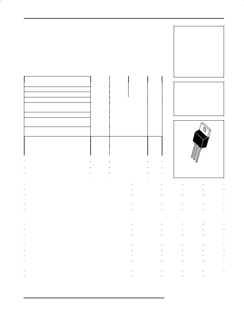
. . . designed for use in general purpose amplifier and switching applications. Compact TO±220 AB package.
MAXIMUM RATINGS
NPN
TIP29B
TIP29C
PNP
TIP30B
TIP30C
|
|
TIP29B |
TIP29C |
|
Rating |
Symbol |
TIP30B |
TIP30C |
Unit |
Collector±Emitter Voltage |
VCEO |
80 |
100 |
Vdc |
Collector±Base Voltage |
VCB |
80 |
100 |
Vdc |
Emitter±Base Voltage |
VEB |
|
5.0 |
Vdc |
Collector Current Ð Continuous |
IC |
|
1.0 |
Adc |
Peak |
|
|
3.0 |
|
Base Current |
IB |
|
0.4 |
Adc |
Total Power Dissipation @ TC = 25_C |
PD |
|
30 |
Watts |
Derate above 25_C |
|
|
0.24 |
W/_C |
Total Power Dissipation @ TA = 25_C |
PD |
|
2.0 |
Watts |
Derate above 25_C |
|
|
0.016 |
W/_C |
Unclamped Inductive Load Energy |
E |
32 |
mJ |
(See Note 3) |
|
|
|
|
|
|
|
Operating and Storage Junction |
TJ, Tstg |
± 65 to +150 |
_C |
Temperature Range |
|
|
|
|
|
|
|
THERMAL CHARACTERISTICS
Characteristic |
Symbol |
Max |
Unit |
|
|
|
|
Thermal Resistance, Junction to Ambient |
RθJA |
62.5 |
_C/W |
Thermal Resistance, Junction to Case |
RθJC |
4.167 |
_C/W |
1 AMPERE
POWER TRANSISTORS COMPLEMENTARY SILICON
80 ± 100 VOLTS
30 WATTS
CASE 221A±06
TO±220AB
ELECTRICAL CHARACTERISTICS (TC = 25_C unless otherwise noted)
Characteristic |
|
Symbol |
Min |
Max |
Unit |
|
|
|
|
|
|
OFF CHARACTERISTICS |
|
|
|
|
|
|
|
|
|
|
|
Collector±Emitter Sustaining Voltage (1) |
TIP29B, TIP30B |
VCEO(sus) |
80 |
Ð |
Vdc |
(IC = 30 mAdc, IB = 0) |
TIP29C, TIP30C |
|
100 |
Ð |
|
Collector Cutoff Current (VCE = 60 Vdc, IB = 0) |
ICEO |
Ð |
0.3 |
mAdc |
|
Collector Cutoff Current |
|
ICES |
|
|
μAdc |
(VCE = 80 Vdc, VEB = 0) |
TIP29B, TIP30B |
|
Ð |
200 |
|
(VCE = 100 Vdc, VEB = 0) |
TIP29C, TIP30C |
|
Ð |
200 |
|
Emitter Cutoff Current (VBE = 5.0 Vdc, IC = 0) |
|
IEBO |
Ð |
1.0 |
mAdc |
ON CHARACTERISTICS (1) |
|
|
|
|
|
|
|
|
|
|
|
DC Current Gain (IC = 0.2 Adc, VCE = 4.0 Vdc) |
hFE |
40 |
Ð |
Ð |
|
DC Current Gain (IC = 1.0 Adc, VCE = 4.0 Vdc) |
|
15 |
75 |
|
|
Collector±Emitter Saturation Voltage (IC = 1.0 Adc, IB = 125 mAdc) |
VCE(sat) |
Ð |
0.7 |
Vdc |
|
Base±Emitter On Voltage (IC = 1.0 Adc, VCE = 4.0 Vdc) |
VBE(on) |
Ð |
1.3 |
Vdc |
|
DYNAMIC CHARACTERISTICS |
|
|
|
|
|
|
|
|
|
|
|
Current±Gain Ð Bandwidth Product (2) |
|
fT |
3.0 |
Ð |
MHz |
(IC = 200 mAdc, VCE = 10 Vdc, ftest = 1.0 MHz) |
|
|
|
|
|
Small±Signal Current Gain (IC = 0.2 Adc, VCE = 10 Vdc, f = 1.0 kHz) |
hfe |
20 |
Ð |
Ð |
|
(1)Pulse Test: Pulse Width v 300 μs, Duty Cycle v 2.0%.
(2)fT = hfe•ftest.
(3)This rating based on testing with LC = 20 mH, RBE = 100 Ω, VCC = 10 V, IC = 1.8 A, P.R.F = 10 Hz.
REV 1
Motorola, Inc. 1995

TIP29B |
TIP29C |
TIP30B |
TIP30C |
|
||||
|
500 |
|
|
|
|
|
|
|
|
300 |
TJ = 150°C |
|
|
|
|
VCE = 2.0 V |
|
GAIN |
100 |
25°C |
|
|
|
|
|
|
|
|
|
|
|
|
|
||
DC CURRENT |
|
|
|
|
|
|
|
|
70 |
± 55°C |
|
|
|
|
|
||
50 |
|
|
|
|
|
|
|
|
30 |
|
|
|
|
|
|
|
|
, |
|
|
|
|
|
|
|
|
FE |
|
|
|
|
|
|
|
|
h |
|
|
|
|
|
|
|
|
|
10 |
|
|
|
|
|
|
|
|
7.0 |
|
|
|
|
|
|
|
|
5.0 |
0.05 0.07 |
0.1 |
|
0.5 |
0.7 |
1.0 |
3.0 |
|
0.03 |
0.3 |
||||||
|
|
|
IC, COLLECTOR CURRENT (AMP) |
|
||||
|
3.0 |
|
|
|
|
|
|
IB1 = IB2 |
|
|
|
2.0 |
|
|
|
|
|
|
|
||
|
|
|
|
|
ts′ |
|
|
IC/IB = 10 |
|
|
|
1.0 |
|
|
|
|
|
|
ts′= ts ± 1/8 tf |
|
|
|
|
|
|
|
|
|
TJ = 25°C |
|
||
|
0.7 |
|
tf @ VCC = 30 V |
|
|
|
|
|||
|
|
|
|
|
|
|
|
|||
μs) |
0.5 |
|
|
|
|
|
|
|
|
|
|
|
|
|
|
|
|
|
|
|
|
( |
|
|
|
|
|
|
|
|
|
|
TIME |
0.3 |
tf @ VCC = 10 V |
|
|
|
|
|
|
|
|
0.2 |
|
|
|
|
|
|
|
|
|
|
t, |
|
|
|
|
|
|
|
|
|
|
|
|
|
|
|
|
|
|
|
|
|
|
0.1 |
|
|
|
|
|
|
|
|
|
|
0.07 |
|
|
|
|
|
|
|
|
|
|
0.05 |
|
|
|
|
|
|
|
|
|
|
0.03 |
|
|
|
|
|
|
|
|
|
|
0.03 |
0.05 |
0.07 0.1 |
0.2 |
0.3 |
0.5 |
0.7 |
1.0 |
2.0 |
3.0 |
|
|
|
IC, COLLECTOR CURRENT (AMP) |
|
|
|||||
Figure 1. DC Current Gain |
Figure 2. Turn±Off Time |
|
TURN±ON PULSE |
VCC |
|
|
APPROX |
RC |
|
||
|
|
|||
+11 V |
|
|
|
|
|
|
|
|
|
Vin 0 |
Vin |
|
SCOPE |
|
|
|
|||
VEB(off) |
|
RB |
|
|
t1 |
|
|
|
|
|
|
|
|
|
APPROX |
t3 |
Cjd << Ceb |
|
|
|
|
± 4.0 V |
|
|
+11 V |
|
t1 ≤ 7.0 ns |
|
|
|
|
|
||
|
|
100 < t2 < 500 ms |
|
|
Vin |
|
t3 < 15 ns |
|
|
|
|
DUTY CYCLE ≈ 2.0% |
|
|
|
t2 |
APPROX ±9.0 V |
|
|
|
TURN±OFF PULSE |
RB and RC VARIED TO OBTAIN |
||
|
|
DESIRED CURRENT LEVELS. |
||
Figure 3. Switching Time Equivalent Circuit
|
10 |
TJ = 150°C |
|
|
|
|
(AMPS) |
|
|
|
|
|
|
3.0 |
|
|
|
|
1 ms |
|
CURRENT |
|
|
|
|
||
|
|
|
|
|
||
0.1 |
|
|
|
dc |
|
|
|
|
|
|
|
||
,COLLECTOR |
|
|
|
|
|
|
|
SECOND BREAKDOWN LIMITED |
|
5 ms |
|||
|
THERMALLY LIMITED @ TC = 25°C |
|
||||
|
BONDING WIRE LIMITED |
|
|
|
||
CURVES APPLY BELOW |
|
|
|
|
||
C |
|
|
|
|
||
I |
RATED VCEO |
|
TIP29B, 30B |
|
||
|
|
|
||||
|
0.1 |
|
|
TIP29C, 30C |
|
|
|
4.0 |
10 |
20 |
40 |
100 |
|
|
1.0 |
|||||
VCE, COLLECTOR±EMITTER VOLTAGE, (VOLTS)
Figure 5. Active Region Safe Operating Area
|
2.0 |
|
|
|
|
|
|
|
|
1.0 |
|
|
|
|
|
|
IC/IB = 10 |
|
|
|
|
|
|
|
TJ = 25°C |
|
|
0.7 |
tr @ VCC = 30 V |
|
|
|
|
||
|
|
|
|
|
|
|||
|
0.5 |
|
|
|
|
|
|
|
( μs) |
0.3 |
tr @ VCC = 10 V |
|
|
|
|
|
|
t, TIME |
0.1 |
|
|
|
|
|
|
|
|
|
|
td @ VEB(off) = 2.0 V |
|
||||
|
0.07 |
|
|
|
||||
|
|
|
|
|
|
|
|
|
|
0.05 |
|
|
|
|
|
|
|
|
0.03 |
|
|
|
|
|
|
|
|
0.02 |
0.05 0.07 |
0.1 |
0.3 |
0.5 |
0.7 |
1.0 |
3.0 |
|
0.03 |
|||||||
|
|
|
IC, COLLECTOR CURRENT (AMP) |
|
||||
Figure 4. Turn±On Time
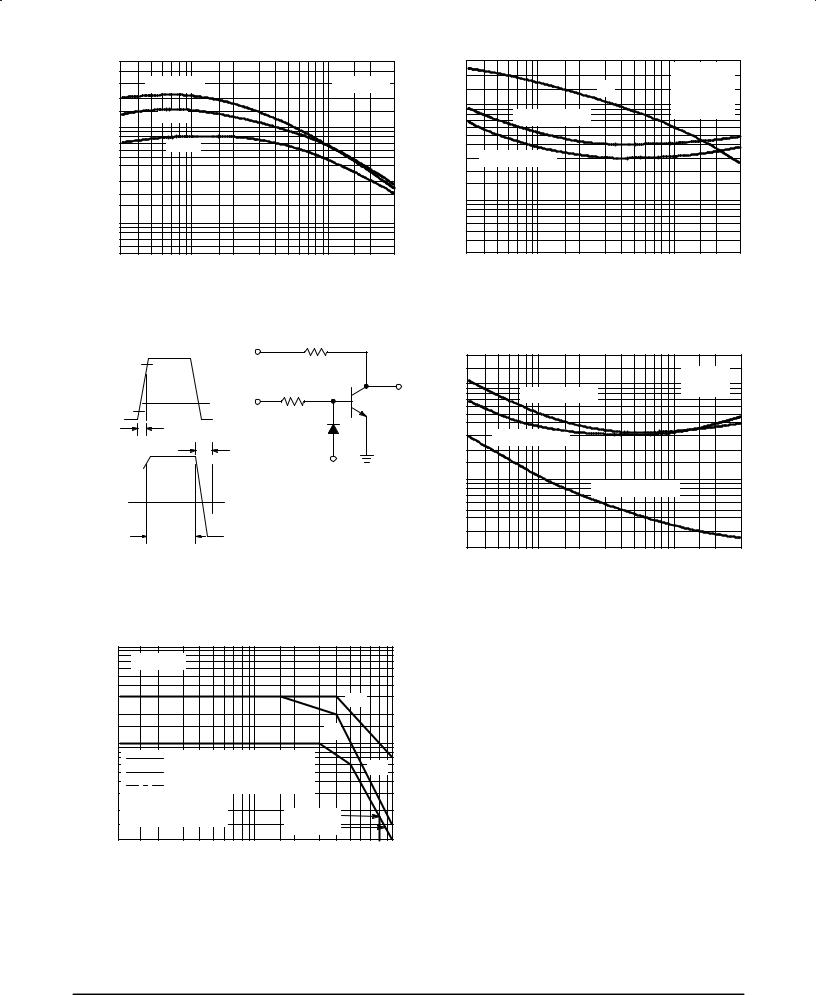
There are two limitations on the power handling ability of a transistor: average junction temperature and second breakdown. Safe operating area curves indicate IC ± VCE operation; i.e., the transistor must not be subjected to greater dissipation than the curves indicate.
The data of Figure 5 is based on TJ(pk) = 150_C; TC is variable depending on conditions. Second breakdown pulse
limits are valid for duty cycles to 10% provided TJ(pk) v 150_C. At high case temperatures, thermal limitations will
reduce the power that can be handled to values less than the limitations imposed by second breakdown.
2 |
Motorola Bipolar Power Transistor Device Data |
 Loading...