


MOTOROLA
SEMICONDUCTOR TECHNICAL DATA
Order this document by TIP120/D
Plastic Medium-Power
Complementary Silicon Transistors
. . . designed for general±purpose amplifier and low±speed switching applications.
• High DC Current Gain Ð
hFE = 2500 (Typ) @ IC = 4.0 Adc
• Collector±Emitter Sustaining Voltage Ð @ 100 mAdc
VCEO(sus) = 60 Vdc (Min) Ð TIP120, TIP125
VCEO(sus) = 80 Vdc (Min) Ð TIP121, TIP126
VCEO(sus) = 100 Vdc (Min) Ð TIP122, TIP127
• Low Collector±Emitter Saturation Voltage Ð
VCE(sat) = 2.0 Vdc (Max) @ IC = 3.0 Adc
VCE(sat) = 4.0 Vdc (Max) @ IC = 5.0 Adc
•Monolithic Construction with Built±In Base±Emitter Shunt Resistors
•TO±220AB Compact Package
*MAXIMUM RATINGS
NPN
TIP120* TIP121*
TIP122*
PNP
TIP125* TIP126* TIP127*
*Motorola Preferred Device
|
|
TIP120, |
TIP121, |
TIP122, |
|
Rating |
Symbol |
TIP125 |
TIP126 |
TIP127 |
Unit |
Collector±Emitter Voltage |
VCEO |
60 |
80 |
100 |
Vdc |
Collector±Base Voltage |
VCB |
60 |
80 |
100 |
Vdc |
Emitter±Base Voltage |
VEB |
|
5.0 |
|
Vdc |
Collector Current Ð Continuous |
IC |
|
5.0 |
|
Adc |
Peak |
|
|
8.0 |
|
|
Base Current |
IB |
|
120 |
|
mAdc |
Total Power Dissipation @ TC = 25_C |
PD |
|
65 |
|
Watts |
Derate above 25_C |
|
|
0.52 |
|
W/_C |
Total Power Dissipation @ TA = 25_C |
PD |
|
2.0 |
|
Watts |
Derate above 25_C |
|
|
0.016 |
|
W/_C |
Unclamped Inductive Load Energy (1) |
E |
|
50 |
|
mJ |
Operating and Storage Junction, |
TJ, Tstg |
|
± 65 to +150 |
|
_C |
Temperature Range |
|
|
|
|
|
THERMAL CHARACTERISTICS
|
Characteristic |
|
|
|
Symbol |
|
Max |
Unit |
||
Thermal Resistance, Junction to Case |
|
|
RθJC |
|
1.92 |
_C/W |
||||
Thermal Resistance, Junction to Ambient |
|
RθJA |
|
62.5 |
_C/W |
|||||
(1) IC = 1 A, L = 100 mH, P.R.F. = 10 Hz, VCC = 20 V, RBE = 100 Ω. |
|
|
||||||||
|
TA |
TC |
|
|
|
|
|
|
|
|
|
4.0 |
80 |
|
|
|
|
|
|
|
|
(WATTS) |
3.0 |
60 |
|
|
|
|
|
|
|
|
|
|
|
|
|
|
|
|
|
|
|
DISSIPATION |
|
|
|
|
|
TC |
|
|
|
|
2.0 |
40 |
|
|
|
|
|
|
|
|
|
|
|
|
|
|
|
|
|
|
|
|
, POWER |
1.0 |
20 |
|
|
|
TA |
|
|
|
|
|
|
|
|
|
|
|
|
|||
|
|
|
|
|
|
|
|
|
|
|
D |
|
|
|
|
|
|
|
|
|
|
P |
|
|
|
|
|
|
|
|
|
|
|
0 |
0 |
20 |
40 |
60 |
80 |
100 |
120 |
140 |
160 |
|
|
0 |
||||||||
|
|
|
|
|
T, TEMPERATURE (°C) |
|
|
|
||
DARLINGTON
5 AMPERE
COMPLEMENTARY SILICON POWER TRANSISTORS
60 ± 80 ± 100 VOLTS
65 WATTS
CASE 221A±06
TO±220AB
Figure 1. Power Derating
Preferred devices are Motorola recommended choices for future use and best overall value.
REV 2
Motorola, Inc. 1995
TIP120 |
TIP121 |
TIP122 |
TIP125 |
TIP126 |
TIP127 |
|
|
|
|
|
|
ELECTRICAL CHARACTERISTICS (TC = 25_C unless otherwise noted) |
|
|
|
|
|||||
|
|
|
|
|
|
|
|
|
|
|
|
|
|
Characteristic |
|
|
Symbol |
Min |
Max |
Unit |
|
|
|
|
|
|
|
|
|
|
||
|
OFF CHARACTERISTICS |
|
|
|
|
|
|
|
||
|
|
|
|
|
|
|
|
|||
|
Collector±Emitter Sustaining Voltage (1) |
|
|
VCEO(sus) |
|
|
Vdc |
|||
|
(IC = 100 mAdc, IB = 0) |
|
TIP120, TIP125 |
|
60 |
Ð |
|
|||
|
|
|
|
|
TIP121, TIP126 |
|
80 |
Ð |
|
|
|
|
|
|
|
TIP122, TIP127 |
|
100 |
Ð |
|
|
|
|
|
|
|
|
|
|
|
|
|
|
Collector Cutoff Current |
|
|
|
|
ICEO |
|
|
mAdc |
|
|
|
|
|
|
|
|
||||
|
(VCE = 30 Vdc, IB = 0) |
|
TIP120, TIP125 |
|
Ð |
0.5 |
|
|||
|
(VCE = 40 Vdc, IB = 0) |
|
TIP121, TIP126 |
|
Ð |
0.5 |
|
|||
|
(VCE = 50 Vdc, IB = 0) |
|
TIP122, TIP127 |
|
Ð |
0.5 |
|
|||
|
Collector Cutoff Current |
|
|
|
|
ICBO |
|
|
mAdc |
|
|
(VCB = 60 Vdc, IE = 0) |
|
TIP120, TIP125 |
|
Ð |
0.2 |
|
|||
|
(VCB = 80 Vdc, IE = 0) |
|
TIP121, TIP126 |
|
Ð |
0.2 |
|
|||
|
(VCB = 100 Vdc, IE = 0) |
|
TIP122, TIP127 |
|
Ð |
0.2 |
|
|||
|
Emitter Cutoff Current |
|
|
|
|
IEBO |
Ð |
2.0 |
mAdc |
|
|
(VBE = 5.0 Vdc, IC = 0) |
|
|
|
|
|
|
|
||
|
ON CHARACTERISTICS (1) |
|
|
|
|
|
|
|
||
|
|
|
|
|
|
|
|
|
|
|
|
DC Current Gain |
|
|
|
|
hFE |
|
|
Ð |
|
|
(IC = 0.5 Adc, VCE = 3.0 Vdc) |
|
|
|
|
1000 |
Ð |
|
||
|
(IC = 3.0 Adc, VCE = 3.0 Vdc) |
|
|
|
|
1000 |
Ð |
|
||
|
Collector±Emitter Saturation Voltage |
|
|
|
VCE(sat) |
|
|
Vdc |
||
|
(IC = 3.0 Adc, IB = 12 mAdc) |
|
|
|
|
Ð |
2.0 |
|
||
|
(IC = 5.0 Adc, IB = 20 mAdc) |
|
|
|
|
Ð |
4.0 |
|
||
|
Base±Emitter On Voltage |
|
|
|
VBE(on) |
Ð |
2.5 |
Vdc |
||
|
(IC = 3.0 Adc, VCE = 3.0 Vdc) |
|
|
|
|
|
|
|
||
|
DYNAMIC CHARACTERISTICS |
|
|
|
|
|
|
|
||
|
|
|
|
|
|
|
|
|
||
|
Small±Signal Current Gain |
|
|
|
hfe |
4.0 |
Ð |
Ð |
||
|
(IC = 3.0 Adc, VCE = 4.0 Vdc, f = 1.0 MHz) |
|
|
|
|
|
|
|||
|
Output Capacitance |
|
|
|
|
Cob |
|
|
pF |
|
|
(VCB = 10 Vdc, IE = 0, f = 0.1 MHz |
|
TIP125, TIP126, TIP127 |
|
Ð |
300 |
|
|||
|
|
|
|
|
TIP120, TIP121, TIP122 |
|
Ð |
200 |
|
|
|
|
|
|
|
|
|
|
|
|
|
(1) Pulse Test: Pulse Width v 300 μs, Duty Cycle v 2%.
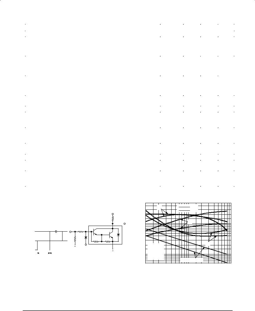
RB & RC VARIED TO OBTAIN DESIRED CURRENT LEVELS |
VCC |
|
|
||
± 30 V |
|
|
|||
D1 MUST BE FAST RECOVERY TYPE, eg: |
|
|
|
|
|
1N5825 USED ABOVE IB ≈ 100 mA |
RC |
|
|
||
MSD6100 USED BELOW IB ≈ 100 mA |
SCOPE |
||||
|
|
||||
TUT |
|
|
|
|
|
|
|
|
|
||
V2 |
|
|
R |
|
|
approx |
|
B |
|
|
|
|
|
|
|
||
+ 8.0 |
V |
|
|
|
|
|
0 |
51 |
D1 |
≈ 8.0 k |
≈ 120 |
|
|
|
|
|
|
V1 |
|
|
|
|
|
|
|
|
+ 4.0 V |
|||||
|
|
|
|
|
|
|
|
|||||||
approx |
|
|
|
|
|
|
|
|
|
|||||
|
|
|
|
|
|
|
|
|
|
|
|
|
|
|
±12 V |
|
|
|
μ |
s |
|
|
|
|
|
|
|
|
|
|
|
25 |
|
for td and tr, D1 is disconnected |
||||||||||
tr, tf ≤ 10 ns |
|
|
|
|
and V2 = 0 |
|||||||||
|
|
|
|
For NPN test circuit reverse all polarities. |
||||||||||
DUTY CYCLE = 1.0%
Figure 2. Switching Times Test Circuit
|
5.0 |
|
|
|
|
|
PNP |
|
|
|
|
|
3.0 |
ts |
|
|
|
|
|
|
|
|
|
|
|
|
|
|
NPN |
|
|
|
|
||
|
2.0 |
|
|
|
|
|
|
|
|
|
|
μs) |
1.0 |
|
|
|
|
tf |
|
|
|
|
|
0.7 |
|
|
|
|
|
|
|
|
|
|
|
( |
|
|
|
|
|
|
|
|
|
|
|
t, TIME |
0.5 |
|
|
|
|
|
|
|
|
|
|
0.3 |
|
|
|
|
|
|
|
|
|
|
|
|
|
|
|
|
|
|
tr |
|
|
|
|
|
0.2 |
VCC = 30 V |
|
|
|
|
|
|
|
|
|
|
|
IC/IB = 250 |
|
|
|
|
|
|
|
|
|
|
0.1 |
IB1 = IB2 |
|
|
|
|
|
|
|
|
|
|
0.07 |
TJ = 25°C |
|
|
td @ VBE(off) = 0 |
|
|
|
|
||
|
0.05 |
|
|
|
|
|
|
|
|||
|
0.1 |
0.2 |
0.3 |
0.5 |
0.7 |
1.0 |
2.0 |
3.0 |
5.0 |
7.0 |
10 |
IC, COLLECTOR CURRENT (AMP)
Figure 3. Switching Times
2 |
Motorola Bipolar Power Transistor Device Data |
 Loading...