


TIP120
ON Semiconductor TIP120, TIP121, TIP122, TIP125, TIP126 Service Manual
...
© Semiconductor Components Industries, LLC, 2007
November, 2007 - Rev. 7
1 Publication Order Number:
TIP120/D
TIP120, TIP121, TIP122
(NPN); TIP125, TIP126,
TIP127 (PNP)
Preferred Devices
Plastic Medium-Power
Complementary Silicon
Transistors
Designed for general-purpose amplifier and low-speed switching
applications.
Features
•High DC Current Gain -
h
FE
= 2500 (Typ) @ I
C
= 4.0 Adc
•Collector-Emitter Sustaining Voltage - @ 100 mAdc
V
CEO(sus)
= 60 Vdc (Min) - TIP120, TIP125
= 80 Vdc (Min) - TIP121, TIP126
= 100 Vdc (Min) - TIP122, TIP127
•Low Collector-Emitter Saturation Voltage -
V
CE(sat)
= 2.0 Vdc (Max) @ I
C
= 3.0 Adc
= 4.0 Vdc (Max) @ I
C
= 5.0 Adc
•Monolithic Construction with Built-In Base-Emitter Shunt Resistors
•Pb-Free Packages are Available*
*For additional information on our Pb-Free strategy and soldering details, please
download the ON Semiconductor Soldering and Mounting Techniques
Reference Manual, SOLDERRM/D.
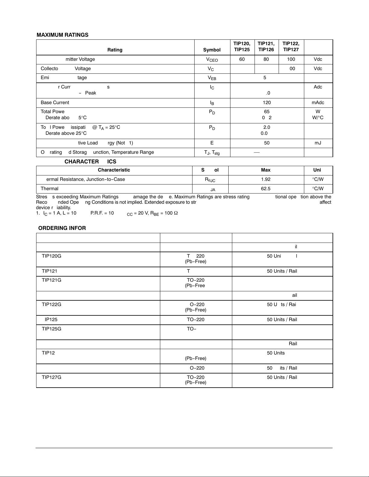
TO-220AB
CASE 221A
STYLE 1
Preferred devices are recommended choices for future use
and best overall value.
MARKING
DIAGRAM
DARLINGTON
5 AMPERE
COMPLEMENTARY SILICON
POWER TRANSISTORS
60-80-100 VOLTS, 65 WATTS
http://onsemi.com
1
2
3
4
TIP12x = Device Code
x = 0, 1, 2, 5, 6, or 7
A = Assembly Location
Y = Year
WW = Work Week
G = Pb-Free Package
TIP12xG
AYWW
See detailed ordering and shipping information in the package
dimensions section on page 2 of this data sheet.
ORDERING INFORMATION
TIP120, TIP121, TIP122 (NPN); TIP125, TIP126, TIP127 (PNP)
http://onsemi.com
2
MAXIMUM RATINGS
Rating
Symbol
TIP120,
TIP125
TIP121,
TIP126
TIP122,
TIP127
Unit
Collector-Emitter Voltage
V
CEO
60
80
100
Vdc
Collector-Base Voltage
V
CB
60
80
100
Vdc
Emitter-Base Voltage
V
EB
5.0
Vdc
Collector Current - Continuous
- Peak
I
C
5.0
8.0
Adc
Base Current
I
B
120
mAdc
Total Power Dissipation @ T
C
= 25°C
Derate above 25°C
P
D
65
0.52
W
W/°C
Total Power Dissipation @ T
A
= 25°C
Derate above 25°C
P
D
2.0
0.016
W
W/°C
Unclamped Inductive Load Energy (Note 1)
E
50
mJ
Operating and Storage Junction, Temperature Range
T
J
, T
stg
–65 to +150
°C
THERMAL CHARACTERISTICS
Characteristic
Symbol
Max
Unit
Thermal Resistance, Junction-to-Case
R
q
JC
1.92
°C/W
Thermal Resistance, Junction-to-Ambient
R
q
JA
62.5
°C/W
Stresses exceeding Maximum Ratings may damage the device. Maximum Ratings are stress ratings only. Functional operation above the
Recommended Operating Conditions is not implied. Extended exposure to stresses above the Recommended Operating Conditions may affect
device reliability.
1. I
C
= 1 A, L = 100 mH, P.R.F. = 10 Hz, V
CC
= 20 V, R
BE
= 100 W
ORDERING INFORMATION
Device Package Shipping
TIP120 TO-220 50 Units / Rail
TIP120G TO-220
(Pb-Free)
50 Units / Rail
TIP121 TO-220 50 Units / Rail
TIP121G TO-220
(Pb-Free)
50 Units / Rail
TIP122 TO-220 50 Units / Rail
TIP122G TO-220
(Pb-Free)
50 Units / Rail
TIP125 TO-220 50 Units / Rail
TIP125G TO-220
(Pb-Free)
50 Units / Rail
TIP126 TO-220 50 Units / Rail
TIP126G TO-220
(Pb-Free)
50 Units / Rail
TIP127 TO-220 50 Units / Rail
TIP127G TO-220
(Pb-Free)
50 Units / Rail
TIP120, TIP121, TIP122 (NPN); TIP125, TIP126, TIP127 (PNP)
http://onsemi.com
3
ELECTRICAL CHARACTERISTICS (T
C
= 25°C unless otherwise noted)
Characteristic
Symbol
Min
Max
Unit
OFF CHARACTERISTICS
Collector-Emitter Sustaining Voltage (Note 2)
(I
C
= 100 mAdc, I
B
= 0) TIP120, TIP125
TIP121, TIP126
TIP122, TIP127
V
CEO(sus)
60
80
100
-
-
-
Vdc
Collector Cutoff Current
(V
CE
= 30 Vdc, I
B
= 0) TIP120, TIP125
(V
CE
= 40 Vdc, I
B
= 0) TIP121, TIP126
(V
CE
= 50 Vdc, I
B
= 0) TIP122, TIP127
I
CEO
-
-
-
0.5
0.5
0.5
mAdc
Collector Cutoff Current
(V
CB
= 60 Vdc, I
E
= 0) TIP120, TIP125
(V
CB
= 80 Vdc, I
E
= 0) TIP121, TIP126
(V
CB
= 100 Vdc, I
E
= 0) TIP122, TIP127
I
CBO
-
-
-
0.2
0.2
0.2
mAdc
Emitter Cutoff Current
(V
BE
= 5.0 Vdc, I
C
= 0)
I
EBO
-
2.0
mAdc
ON CHARACTERISTICS (Note 2)
DC Current Gain
(I
C
= 0.5 Adc, V
CE
= 3.0 Vdc)
(I
C
= 3.0 Adc, V
CE
= 3.0 Vdc)
h
FE
1000
1000
-
-
-
Collector-Emitter Saturation Voltage
(I
C
= 3.0 Adc, I
B
= 12 mAdc)
(I
C
= 5.0 Adc, I
B
= 20 mAdc)
V
CE(sat)
-
-
2.0
4.0
Vdc
Base-Emitter On Voltage
(I
C
= 3.0 Adc, V
CE
= 3.0 Vdc)
V
BE(on)
-
2.5
Vdc
DYNAMIC CHARACTERISTICS
Small-Signal Current Gain
(I
C
= 3.0 Adc, V
CE
= 4.0 Vdc, f = 1.0 MHz)
h
fe
4.0
-
-
Output Capacitance
(V
CB
= 10 Vdc, I
E
= 0, f = 0.1 MHz TIP125, TIP126, TIP127
TIP120, TIP121, TIP122
C
ob
-
-
300
200
pF
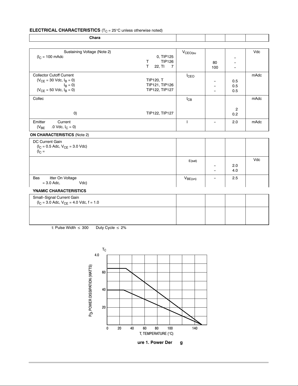
2. Pulse Test: Pulse Width v 300 ms, Duty Cycle v 2%
80
0
0 20 40 60 80 100 120 160
Figure 1. Power Derating
T, TEMPERATURE (°C)
P
D
, POWER DISSIPATION (WATTS)
40
20
60
140
T
C
4.0
0
2.0
1.0
3.0
T
A
T
A
T
C
 Loading...