


ON Semiconductor ST6391, ST6392, ST6393, ST6395, ST6397 Technical data
...ST6391
ST6391, ST6392, ST6393 ST6395, ST6397, ST6399
DATA SHEET
USE IN LIFE SUPPORT DEVICES OR SYSTEMS MUST BE EXPRESSLY AUTHORIZED.
SGS-THOMSON PRODUCTS ARE NOT AUTHORIZED FOR USE AS CRITICAL COMPONENTS IN LIFE SUPPORT DEVICES OR SYSTEMS WITHOUT THE EXPRESS WRITTEN APPROVAL OF SGS-THOMSON Microelectronics.
As used herein :
1.Life support devices or systems are those which (a) are intended for surgical implant into the body, or (b) support or sustain life, and whose failure to perform, when properly used in accordance with instructions for use provided with the product, can be reasonably expected to result in significant injury to the user.
2. A critical component is any component of a life support device or system whose failure to perform can reasonably be expected to cause the failure of the life support device or system, or to affect its safety or effectiveness.

ST639x DATASHEET INDEX
ST6391, ST6392, ST6393 |
Pages |
|
|
ST6395, ST6397, ST6399 . . . . . . . . . . . . . . . . . . . . . . . . . . . . . . . |
1 |
GENERAL DESCRIPTION . . . . . . . . . . . . . . . . . . . . . . . . . . . . . . . . . . . . . . |
3 |
PIN DESCRIPTION . . . . . . . . . . . . . . . . . . . . . . . . . . . . . . . . . . . . . . . . . |
5 |
ST639x CORE . . . . . . . . . . . . . . . . . . . . . . . . . . . . . . . . . . . . . . . . . . . . |
7 |
MEMORY SPACES . . . . . . . . . . . . . . . . . . . . . . . . . . . . . . . . . . . . . . . . . |
10 |
INTERRUPT . . . . . . . . . . . . . . . . . . . . . . . . . . . . . . . . . . . . . . . . . . . . . |
17 |
RESET . . . . . . . . . . . . . . . . . . . . . . . . . . . . . . . . . . . . . . . . . . . . . . . . |
21 |
WAIT & STOP MODES . . . . . . . . . . . . . . . . . . . . . . . . . . . . . . . . . . . . . . . |
23 |
ON-CHIP CLOCK OSCILLATOR . . . . . . . . . . . . . . . . . . . . . . . . . . . . . . . . . . |
24 |
INPUT/OUTPUT PORTS . . . . . . . . . . . . . . . . . . . . . . . . . . . . . . . . . . . . . . |
25 |
TIMERS . . . . . . . . . . . . . . . . . . . . . . . . . . . . . . . . . . . . . . . . . . . . . . . |
28 |
HARDWARE ACTIVATED DIGITAL WATCHDOG FUNCTION . . . . . . . . . . . . . . . . . . . |
31 |
SERIAL PERIPHERAL INTERFACE . . . . . . . . . . . . . . . . . . . . . . . . . . . . . . . . . |
32 |
6-BIT PWM D/A CONVERTERS . . . . . . . . . . . . . . . . . . . . . . . . . . . . . . . . . . . |
41 |
AFC A/D COMPARATOR . . . . . . . . . . . . . . . . . . . . . . . . . . . . . . . . . . . . . . |
41 |
DEDICATED LATCHES . . . . . . . . . . . . . . . . . . . . . . . . . . . . . . . . . . . . . . . |
42 |
ON-SCREEN DISPLAY (OSD) . . . . . . . . . . . . . . . . . . . . . . . . . . . . . . . . . . . . |
43 |
SOFTWARE DESCRIPTION . . . . . . . . . . . . . . . . . . . . . . . . . . . . . . . . . . . . . |
52 |
ABSOLUTE MAXIMUM RATINGS . . . . . . . . . . . . . . . . . . . . . . . . . . . . . . . . . . |
57 |
PACKAGE MECHANICAL DATA . . . . . . . . . . . . . . . . . . . . . . . . . . . . . . . . . . |
61 |
ORDERING INFORMATION TABLE . . . . . . . . . . . . . . . . . . . . . . . . . . . . . . . . . |
64 |
|
|
|
ST6391, ST6392, ST6393 |
|
|
|
ST6395, ST6397, ST6399 |
|
|
|
8-BIT HCMOS MCUs |
|
FOR TV FREQUENCY SYNTHESIS WITH OSD |
||
|
|
|
PRELIMINARY DATA |
4.5 to 6V supply operating range |
|
||
8MHz Maximum Clock Frequency |
|
||
User Program ROM: Up to |
20140 |
bytes |
|
Reserved Test ROM:Up to |
340 |
bytes |
|
Data ROM: |
User selectable size |
||
Data RAM: |
|
256 |
bytes |
Data EEPROM: |
Up to |
384 |
bytes |
42-Pin Shrink Dual in Line Plastic Package
Up to 23 software programmable general purpose Inputs/Outputs, including 2 direct LED driving Outputs
Two Timers each including an 8-bit counter with a 7-bit programmable prescaler
Digital Watchdog Function
1
PSDIP42
(Ordering Information at the end of the datasheet)
Serial Peripheral Interface (SPI) supporting S-BUS/ I2C BUS and standard serial protocols
SPI for external frequency synthesis tuning
Up to Six 6-Bit PWM D/A Converters
AFC A/D converter with 0.5V resolution
Five interrupt vectors (IRIN/NMI, Timer 1 & 2, VSYNC, PWR INT.)
On-chip clock oscillator
5 Lines by 15 Characters On-Screen Display Generator with 128 Characters
All ROM types are supported by pin-to-pin EPROM and OTP versions.
The development tool of the ST639x microcontrollers consists of the ST638x-EMU emulation and development system to be connected via a standard RS232 serial line to an MS-DOS Personal Computer.
DEVICE SUMMARY
DEVICE |
ROM |
EEPROM |
|
(Bytes) |
(Bytes) |
||
|
|||
ST6391 |
16K |
128 |
|
ST6392 |
20K |
128 |
|
ST6393 |
16K |
128 |
|
ST6395 |
20K |
384 |
|
ST6397 |
20K |
384 |
|
ST6399 |
16K |
128 |
October 1993 |
1/64 |
This is Preliminary information from SGS-THOMSON. Details are subject to change without notice.
ST6391,92,93,95,97,99
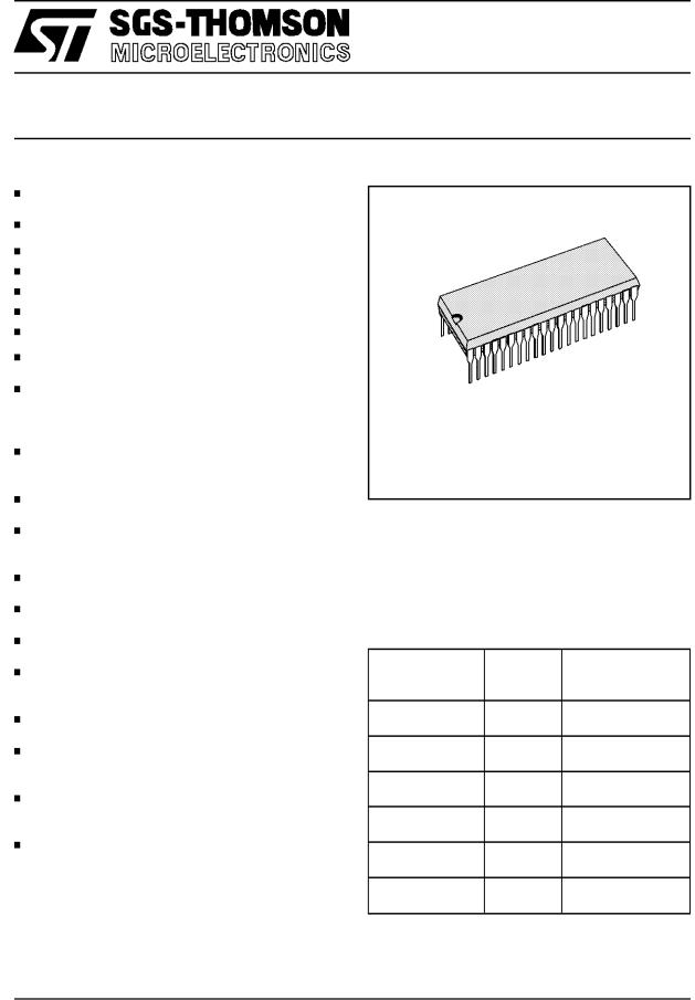
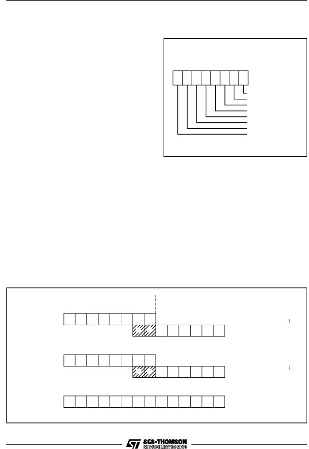
Figure 1. ST6393/97 Pin Configuration
DA0 |
1 |
42 |
V DD |
DA1 |
2 |
41 |
PC0 (SCL) |
DA2 |
3 |
40 |
PC1 (SDA) |
DA3 |
4 |
39 |
PC2 |
DA4 |
5 |
38 |
PC3 (SEN) |
DA5 |
6 |
37 |
PC4 |
PB1 |
7 |
36 |
PC5 |
PB2 |
8 |
35 |
PC6 (IRIN) |
AFC |
9 |
34 |
PC7 |
PB4 |
10 |
33 |
RESET |
PB5 |
11 |
32 |
OSCout |
PB6 |
12 |
31 |
OSCin |
PA0 |
13 |
30 |
TEST |
PA1 |
14 |
29 |
OSDOSCout |
PA2 |
15 |
28 |
OSDOSCin |
PA3 |
16 |
27 |
VSYNC |
PA4 |
17 |
26 |
HSYNC |
PA5 |
18 |
25 |
BLANK |
PA6 |
19 |
24 |
B |
PA7 |
20 |
23 |
G |
VSS |
21 |
22 |
R |
|
|
|
VA00339 |
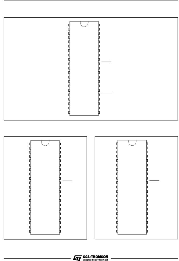
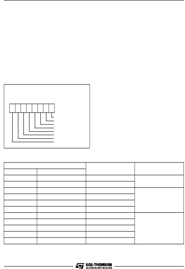
Figure 2. ST6392/99 Pin Configuration |
Figure 3. ST6391/95 Pin Configuration |
||||||
DA0 |
1 |
42 |
V DD |
DA0 |
1 |
42 |
V DD |
DA1 |
2 |
41 |
PC0 (SCL) |
DA1 |
2 |
41 |
PC0 (SCL) |
DA2 |
3 |
40 |
PC1 (SDA) |
DA2 |
3 |
40 |
PC1 (SDA) |
DA3 |
4 |
39 |
PC2 |
DA3 |
4 |
39 |
PC2 |
62.5kHz OUT |
5 |
38 |
PC3 (SEN) |
DA4 |
5 |
38 |
PC3 (SEN) |
PB0 |
6 |
37 |
PC4 (PWRIN) |
PB0 |
6 |
37 |
(1) |
PC4 (PWRIN ) |
|||||||
PB1 |
7 |
36 |
PC5 |
PB1 |
7 |
36 |
PC5 |
PB2 |
8 |
35 |
PC6 (IRIN) |
PB2 |
8 |
35 |
PC6 (IRIN) |
PB3 |
9 |
34 |
PC7 |
PB3 |
9 |
34 |
PC7 |
PB4 |
10 |
33 |
RESET |
PB4 |
10 |
33 |
RESET |
PB5 |
11 |
32 |
OSCout |
PB5 |
11 |
32 |
OSCout |
PB6 |
12 |
31 |
OSCin |
PB6 |
12 |
31 |
OSCin |
PA0 |
13 |
30 |
TEST |
PA0 |
13 |
30 |
TEST |
PA1 |
14 |
29 |
OSDOSCout |
PA1 |
14 |
29 |
OSDOSCout |
PA2 |
15 |
28 |
OSDOSCin |
PA2 |
15 |
28 |
OSDOSCin |
PA3 |
16 |
27 |
VSYNC |
PA3 |
16 |
27 |
VSYNC |
PA4 |
17 |
26 |
HSYNC |
PA4 |
17 |
26 |
HSYNC |
PA5 |
18 |
25 |
BLANK |
PA5 |
18 |
25 |
BLANK |
PA6 (HD0) |
19 |
24 |
B |
PA6 (HD0) |
19 |
24 |
B |
PA7 (HD1) |
20 |
23 |
G |
PA7 (HD1) |
20 |
23 |
G |
VSS |
21 |
22 |
R |
VSS |
21 |
22 |
R |
|
|
|
VA00340 |
|
|
|
VA00337 |
|
|
|
|
Note 1. ST6395 only |
|
|
|
2/64

GENERAL DESCRIPTION
The ST639x microcontrollers are members of the 8- bit HCMOS ST638x family, a series of devices specially oriented to TV applications. Different ROM size and peripheral configurations are available to give the maximum application and cost flexibility. All ST639x members are based on a building block approach:a common core is surrounded bya combination of on-chip peripherals (macrocells) available from a standard library. These peripherals are designed with the same Core technology providing full compatibility and short design time. Many of these macrocells are specially dedicated to TV applications. The macrocells of the ST639x family are: two Timer peripherals each including an 8-bit counter with a 7-bit software programmable prescaler
ST6391,92,93,95,97,99
(Timer), a digital hardware activated watchdog function (DHWD), a 14-bit voltage synthesis tuning peripheral, a Serial Peripheral Interface (SPI), up to six 6-bit PWM D/A converters, an AFC A/D converter with 0.5V resolution, an on-screen display (OSD) with 15 characters per line and 128 characters (in two banks each of 64 characters). In addition the following memory resources are available: program ROM (up to 20K), data RAM (256 bytes), EEPROM (up to 384 bytes). Refer to pin configurations figures and to ST639x device summary (Table 1) for the definition of ST639x family members and a summary of differences among the different types.
3/64

ST6391,92,93,95,97,99
Figure 4. ST6391,92,93, 95,97,99 Block Diagram
TEST
IRIN/PC6
* Refer To Pin Configuration For Additional Information
TEST
IR INTERRUPT
Input
USER PROGRAM
ROM
UP TO 20 kBytes
PC
STACK LEVEL 1 STACK LEVEL 2 STACK LEVEL 3 STACK LEVEL 4 STACK LEVEL 5 STACK LEVEL 6
DATA ROM
USER SELECTABLE
DATA RAM
256 Bytes
DATA EEPROM
384 Bytes
8-BIT CORE
POWER SUPPLY OSCILLATOR |
RESET |
PORT A |
PA0 - PA7 * |
|
PORT B |
PB0 - PB7 * |
|
PORT C |
PC2, PC4 - PC7 * |
|
PC0 / SCL |
||
|
||
|
PC1 / SDA |
|
SERIAL PERIPHERAL |
PC3 / SEN |
|
INTERFACE |
|
|
TIMER 1 |
|
|
TIMER 2 |
|
|
DIGITAL |
|
|
WATCHDOG/TIMER |
|
|
D / A Outputs |
DA0 - DA5 |
|
AFC Input |
AFC |
|
ON-SCREEN |
R, G, B, BLANK |
|
DISPLAY |
HSYNC, VSYNC |
VDD |
VSS |
OSCin OSCout |
RESET |
VR0 1753G |
Table 1. Device Summary
|
ROM |
RAM |
EEPROM |
|
|
COLOUR |
LOW |
PWRIN |
SPI |
62.5kHz |
EMULATING |
|
DEVICE |
AFC |
D/A |
POWER IN |
CLK FREQ. |
||||||||
(Bytes) |
(Bytes) |
(Bytes) |
PINS |
PIN |
Pin |
DEVICES |
||||||
|
|
|
RESET |
(kHz) |
||||||||
|
|
|
|
|
|
|
|
|
|
|||
ST6391 |
16K |
256 |
128 |
NO |
5 |
3 |
NO |
NO |
62.5 |
NO |
ST63E91 |
|
ST6392 |
20K |
256 |
128 |
NO |
4 |
3 |
YES |
YES |
62.5 |
YES |
ST63E92 |
|
ST6393 |
16K |
256 |
128 |
YES |
6 |
3 |
NO |
NO |
62.5 |
NO |
ST63E93 |
|
ST6395 |
20K |
256 |
384 |
NO |
5 |
3 |
NO |
YES |
100 |
NO |
ST63E95 |
|
ST6397 |
20K |
256 |
384 |
YES |
6 |
3 |
NO |
NO |
100 |
NO |
ST63E97 |
|
ST6399 |
16K |
256 |
128 |
NO |
4 |
3 |
YES |
YES |
62.5 |
YES |
ST63E99 |
4/64

PIN DESCRIPTION
VDD and VSS. Power is supplied to the MCU using these two pins. VDD is power and VSS is the ground connection.
OSCin, OSCout. These pins are internally connected to the on-chip oscillator circuit. A quartz crystal or a ceramic resonator can be connected between these two pins in order to allow the correct operation of the MCU with various stability/cost trade-offs. The OSCin pin is the input pin, the OSCout pin is the output pin.
RESET. The active low RESET pin is used to start the microcontroller to the beginning of its program. Additionally the quartz crystal oscillator will be disabled when the RESET pin is low to reduce power consumption during reset phase (ST6392/99 only).
TEST. The TEST pin must be held at VSS for normal operation.
PA0-PA7. These 8 lines are organized as one I/O port (A). Each line may be configured as either an input with or without pull-up resistor or as an output under software control of the data direction register. Pins PA4 to PA7 are configured as open-drain outputs (12V drive). On PA4-PA7 pins the input pull-up option is not available while PA6 and PA7 have additional current driving capability (25mA, VOL:1V). PA0 to PA3 pins are configured as pushpull.
PB0-PB2, PB4-PB6. These 6 lines are organized as one I/O port (B). Each line may be configured as either an input with or without internal pull-up resistor or as an output under software control of the data direction register.
PC0-PC7. These 8 lines are organized as one I/O port (C). Each line may be configured as either an input with or without internal pull-up resistor or as an output under software control of the data direction register. Pins PC0 to PC3 are configured as open-drain (5V drive) in output mode while PC4 to PC7 are open-drain with 12V drive and the input pull-up options does not exist on these four pins.
PC0, PC1 and PC3 lines when in output mode are ªANDedº with the SPI control signals and are all
ST6391,92,93,95,97,99
Open-drain. PC0 is connected to the SPI clock signal (SCL), PC1 with the SPI data signal (SDA) while PC3 is connected with SPI enable signal (SEN, used in S-BUS protocol). Pin PC4 and PC6 can also be inputs to software programmable edge sensitive latches which can generate interrupts; PC4 can be connected to Power Interrupt while PC6 can be connected to the IRIN/NMI interrupt line.
DA0-DA5. These pins are the six PWM D/A outputs of the 6-bit on-chip D/A converters. These lines have open-drain outputs with 12V drive. The output repetition rate is 31.25KHz (with 8MHz clock).
AFC. This is the input of the on-chip 10 levels comparator that can be used to implement the AFC function. This pin is an high impedance input able to withstand signals with a peak amplitude up to 12V.
OSDOSCin, OSDOSCout. These are the On Screen Display oscillator terminals. An oscillation capacitor and coil network have to be connected to provide the right signal to the OSD.
HSYNC, VSYNC. These are the horizontal and vertical synchronization pins. The active polarity of these pins to the OSD macrocell can be selected by the user as ROM mask option. If the device is specified to have negative logic inputs, then these signals are low the OSD oscillator stops. If the device is specified to have positive logic inputs, then when these signals are high the OSD oscillator stops.
R, G, B, BLANK. Outputs from the OSD. R, G and B are the color outputs while BLANK is the blanking output. All outputs are push-pull. The active polarity of these pins can be selected by the user as ROM mask option.
62.5kHz OUT. This pin is available only on the ST6392/99. The pin is an open drain (12V) output at the frequency of 62.5kHz (with an 8MHz clock). The pin can be used to drive the SGS-THOMSON TEA5640 Chroma Processor. Refer to the TEA5640 Data sheet for more information.
5/64
ST6391,92,93,95,97,99
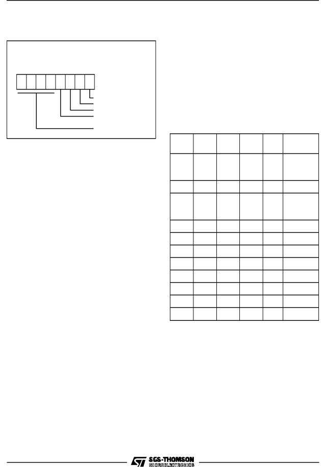
Table 2. Pin Summary
Pin Function |
Description |
DA0 to DA5 |
Output, Open-Drain, 12V |
AFC |
Input, High Impedance, 12V |
R,G,B, BLANK |
Output, Push-Pull |
HSYNC, VSYNC |
Input, Pull-up, Schmitt Trigger |
OSDOSCin |
Input, High Impedance |
OSDOSCout |
Output, Push-Pull |
TEST |
Input, Pull-Down |
OSCin |
Input, Resistive Bias, Schmitt Trigger to Reset Logic Only |
OSCout |
Output, Push-Pull |
RESET |
Input, Pull-up, Schmitt Trigger Input |
PA0-PA3 |
I/O, Push-Pull, Software Input Pull-up, Schmitt Trigger Input |
PA4-PA5 |
I/O, Open-Drain, 12V, No Input Pull-up, Schmitt Trigger Input |
PA6-PA7 |
I/O, Open-Drain, 12V, No Input Pull-up, Schmitt Trigger Input, High Drive |
PB0-PB6 |
I/O, Push-Pull, Software Input Pull-up, Schmitt Trigger Input |
PC0-PC3 |
I/O, Open-Drain, 5V , Software Input Pull-up, Schmitt Trigger Input |
PC4-PC7 |
I/O, Open-Drain, 12V, No Input Pull-up, Schmitt Trigger Input |
VDD, VSS |
Power Supply Pins |
62.5kHz OUT |
Output, Open-Drain 12V |
6/64
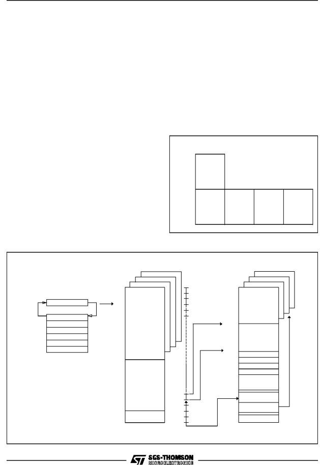
ST639x CORE
The Core of the ST639x Family is implemented independently from the I/O or memory configuration. Consequently, it can be treated as an independent centralprocessor communicating with I/O and memory via internal addresses, data, and control busses. The in-core communication is arranged as shown in the following block diagram figure; the controller being externallylinked to both the reset and the oscillator, while the core is linked to the dedicated onchip macrocells peripherals via the serial data bus and indirectly for interrupt purposes through the control registers.
Registers
The ST639x Family Core has five registers and three pairs of flags available to the programmer. They are shown in Figure 5 and are explained in the following paragraphs together with the program and data memory page registers.
Accumulator (A). The accumulator is an 8-bit general purpose register used in all arithmetic calculations, logical operations, and data manipulations. The accumulator is addressed in the data space as RAM location at the FFh address.
Accordingly, the ST639x instruction set can use the accumulator as any other register of the data space.
Figure 5. ST639x Core Block Diagram
ST6391,92,93,95,97,99
Figure 6. ST639x Core Programming Model
INDEX |
b7 |
X REG. POINTER |
b0 |
SHORT |
|
|
|
|
|
||
REGISTER |
b7 |
Y REG. POINTER |
b0 |
DIRECT |
|
|
ADDRESSING |
||||
|
|
|
|
|
|
|
b7 |
V REGISTER |
b0 |
MODE |
|
|
b7 |
W REGISTER |
|
b0 |
|
|
b7 |
ACCUMULATOR |
b0 |
|
|
b11 |
PROGRAM COUNTER |
|
b0 |
|
|
|
SIX LEVELS |
|
|
|
|
|
STACK REGISTER |
|
|
|
|
NORMAL FLAGS |
|
C |
Z |
|
|
INTERRUPT FLAGS |
C |
Z |
|
||
NMI FLAGS |
|
C |
Z |
|
|
|
|
|
|
|
VA000423 |
7/64

ST6391,92,93,95,97,99
ST639x CORE (Continued)
Indirect Registers (X, Y). These two indirect registers are used as pointers to the memory locations in the data space. They are used in the register-in- direct addressing mode.These registers can be addressed in the data space as RAM locations at the 80h (X) and 81h (Y) addresses. They can also be accessed with the direct, short direct, or bit direct addressing modes. Accordingly, the ST639x instruction set can use the indirect registers as any other register of the data space.
Short Direct Registers (V, W). These two registers are used to save one byte in short direct addressing mode. These registers can be addressed in the data space as RAM locations at the 82h (V) and 83h (W) addresses. They can also be accessed with the direct and bit direct addressing modes. Accordingly, the ST639x instruction set can use the short direct registers as any other register of the data space.
Program Counter (PC)
The program counteris a 12-bit register thatcontains the address of the next ROM location to be processed by the core. This ROM location may be an opcode, an operand, or an address of operand. The 12-bit length allows the direct addressing of 4096 bytes in the program space. Nevertheless, if the program space contains more than 4096 locations, the further program space can be addressed by using the Program ROM Page Register. The PC value is incremented, after it is read for the address of the current instruction, by sending it through the ALU, so giving the address of the next byte in the program. To execute relative jumps the PC and the offset values are shifted through the ALU, where they will be added, and the result is shifted backinto the PC. The program counter can be changed in the following ways:
JP (Jump) instruction.... |
PC= Jump address |
CALL instruction ........... |
PC=Call address |
Relative Branch |
|
instructions ................... |
PC=PC+offset |
Interrupt........................ |
PC=Interrupt vector |
Reset............................ |
PC=Reset vector |
RET & RETI instructions |
............PC=Pop (stack) |
Normal instruction ........ |
PC= PC+1 |
8/64
Flags (C, Z)
The ST639x Core includes three pairs of flags that correspond to 3 different modes: normal mode, interrupt mode and Non-Maskable-Interrupt-Mode. Each pair consists of a CARRY flag and a ZERO flag. One pair (CN, ZN) is used during normal operation, one pair is used during the interrupt mode (CI,ZI) and one is used during the not-maskable interrupt mode (CNMI, ZNMI).
The ST639x Core uses the pair of flags that corresponds to the actual mode: as soon as an interrupt (resp. a Non-Maskable-Interrupt) is generated, the ST639x Core uses the interrupt flags (resp. the NMI flags) instead of the normal flags. When the RETI instruction is executed, the normal flags (resp. the interrupt flags) are restored if the MCU was in the normal mode(resp. in the interrupt mode)before the interrupt. Should be observed that each flag set can only be addressed in its own routine (Not-maskable interrupt, normal interrupt or main routine). The interrupt flags are not cleared during the context switching and so, theyremain in the state they were at the exit of the last routine switching.
The Carry flag is set when a carry or a borrow occurs during arithmetic operations, otherwise it is cleared. The Carry flag is also set to the value of the bit tested in a bit test instruction, and participates in the rotate left instruction.
The Zero flag is set if the result of the last arithmetic or logical operation was equal to zero, otherwise it is cleared.
The switching between these three sets is automatically performed when an NMI, an interrupt and a RETI instructions occur. As the NMI mode is automatically selected after the reset of the MCU, the ST639x Core uses at first the NMI flags.
Figure 7. Stack Operation
WHEN
RET OR RETI
OCCURS
PROGRAM COUNTER
STACK LEVEL 1
STACK LEVEL 2
STACK LEVEL 3
STACK LEVEL 4
STACK LEVEL 5
STACK LEVEL 6
WHEN CALL
OR
INTERRUPT REQUEST
OCCURS
VA000424
ST639x CORE (Continued)
Stack
The ST639x Core includes true LIFO hardware stack that eliminates the need for a stack pointer. The stack consists of six separate 12-bit RAM locations that do not belong to the data space RAM area. When a subroutine call (or interrupt request) occurs, the contents of each level is shifted into the next level while the content of the PC is shifted into the first level (the value of the sixth level will be lost). When subroutine or interrupt return occurs (RET or RETI instructions), the first level register is shifted back into the PC and the value of each level is shifted back into the previous level. These two operating modes are described in Figure 7. Since the accumulator, as all other data space registers, is not stored in this stack the handling of this registers shall be performed inside the subroutine. The stack pointer will remain in its deepest position, if more than 6 calls or interrupts are executed, so that the last return address will be lost. It will also remain in its highest position if the stack is empty and a RET or RETI is executed. In this case the next instruction will be executed.
Memory Registers
The PRPR can be addressed like a RAM location in the Data Space at the CAh address; nevertheless it is a write-only register that can not be accessed with single-bit operations. This register is used to select the 2-Kbyte ROM bank of the Program Space that will be addressed. The number of the page has to be loaded in the PRPR. The PRPR is not cleared during the MCU initialization and should therefore be defined before jumping out of the static page. Refer to the Program Space description for additional information concerning the use of this register. The PRPR is not modified when an interrupt or a subroutine occurs.
Figure 8. Program ROM Page Register
PRPR
Program ROM Page Register
(CAh, Write Only)
D7 D6 D5 D4 D3 D2 D1 D0
ST6391,92,93,95,97,99
The DRBR can be addressed like a RAM location in the Data Space at the E8h address, nevertheless it is write-only register that can not be accessed with single-bit operations. This register is used to select the desired 64-byte RAM/EEPROM bank of the Data Space. The number of the bank has to be loaded in the DRBR and the instruction has to point to the selected location as it was in the 0 bank (from 00h address to 3Fh address). This register is undefined after Reset. Refer to the Data Space description for additional information. The DRBR register is not modified when a interrupt or a subroutine occurs.
Figure 9. Data RAM Bank Register
DRBR
Data RAM Bank Register
(E8h, Write Only)
D7 |
D6 |
D5 |
D4 |
D3 |
D2 |
D1 |
D0 |
The DRWR register can be addressedlike a RAM location in the Data Space at the C9h address, nevertheless it is write-only register that can not be accessed with single-bit operations. This register is used to move up and down the 64-byte read-only data window (from the 40h address to 7Fh address of the Data Space) along the ROM of the MCU by step of 64 bytes. The effective address of the byte to be read as a data in the ROM is obtainedby the concatenationof the 6 less significant bits of the address given in the instruction (as less significant bits) and the content of the DRWR (as most significant bits). Refer to the Data Space description for additional information.
Figure 10. Data ROM Window Register
DRWR
Data ROM Window Register
(C9h, Write Only)
D7 |
D6 |
D5 |
D4 |
D3 |
D2 |
D1 |
D0 |
9/64
ST6391,92,93,95,97,99
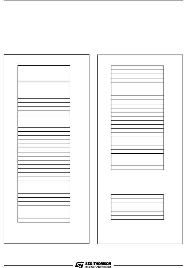
MEMORY SPACES
The MCUs operate in three different memory spaces: Stack Space, Program Space, and Data Space. A description of these spaces is shown in Figure 11.
Stack Space
The stack space consists of six 12 bit registers that are used for stacking subroutine and interrupt return addressesplus the current programcounterregister.
Program Space
The program space is physically implemented in the ROM and includes all the instructions that are to be executed, as well as the data required for the immediate addressing mode instructions, the reserved test area and user vectors. It is addressed thanks to the 12-bit Program Counter register (PC register) and so, the ST639x Core can directly address up to 4K bytes of Program Space. Nevertheless, the Program Space can be extended by the addition of 2-Kbyte ROM banks as it is shown in Figure 13 in which a 20K bytes memory is described. These banks are addressed by pointing to the 000h-7FFh locations of the Program Space thanks to the Program Counter, and by writing the appropriate code in the Program ROM Page Register (PRPR) located at the CAh address of the Data Space. Because interrupts and common subroutines should be available all the time only the
lower 2K byte of the 4K program space are bank switched while the upper 2K byte can be seen as static space. Table 3 gives the different codes that allows the selection of the corresponding banks. Note that, from the memory point of view, the Page 1 and the Static Page represent the same physical memory: it is only a different way of addressing the same location. On the ST6392,95,97, a total of 2048, bytes of ROM have been implemented; 20140 are available as user ROM while 340 are reserved for testing.
Figure 12. ST639x 20K Bytes Program Space
Addressing Description
Program
counter 0000h 4FFFh space
0FFFh
Static Page
Page 1
0800h
07FFh
Page 0 |
Page 1 |
Page 9 |
|
Static Page |
|||
|
|
0000h
Figure 11. ST639x Memory Addressing Description Diagram
STACK SPACE |
PROGRAM SPACE |
00 00h |
000h |
PROGRAM COUNTER |
|
STACK LEVE L 1 STACK LEVE L 2 STACK LEVE L 3 STACK LEVE L 4 STACK LEVE L 5 STACK LEVE L 6
0-63
03Fh
ROM
040h
070h
07FFh
080h
081h
08 00h 082h
083h
084h
DATA SPACE
RAM / E EPROM
B AN KING AREA
DATA ROM
WINDO W
XRE GISTER
YREGISTER
VRE GISTER W REGISTER
R AM
|
ROM |
0C0 h |
0FF0h |
|
|
|
INTERRU PT & |
|
0FFFh |
RESET VECTORS |
0FFh |
|
|
DATA ROM
WI NDOW SELECT
DATA RAM
BANK SELEC T
ACCUMULATOR
VR001568
10/64
MEMORY SPACES (Continued)
Figure 13. Program ROM Page Register
PRPR
Program ROM Page Register
(CAh, Write Only)
D7 D6 D5 D4 D3 D2 D1 D0
PRPR0
PRPR1
PRPR2
PRPR3
UNUSED
D7-D5. These bits are not used.
PRPR4-PRPR0. These are the program ROM banking bits and the value loaded selects the corresponding page to be addressed in the lower part of 4K program address space as specified in Table 3. This register is undefined on reset.
Note. The number of bits implemented depends on the size of the ROM of the device. Only the lower part of address space has been bankswitched because interrupt vectors and common subroutines should be available all the time. The reason of this structure is due to the fact that it is not possible to jump from a dynamic page to another, unless jumping back to the static page, changing contents of PRPR, and, than, jumping to a different dynamic page.
Care is required when handling the PRPR as it is write only. For this reason, it is not allowed to change the PRPR contents while executing interrupts drivers, as the driver cannot save and than restore its previous content. Anyway, this operation may be necessary if the sum of common routines and interrupt drivers will take more than 2K bytes; in this case could be necessary to divide the
ST6391,92,93,95,97,99
interrupt driver in a (minor) part in the static page (start and end), and in the second (major) part in one dynamic page. If it is impossible to avoid the writing of this register in interrupts drivers, an image of this register must be saved in a RAM location, and each time the program writes the PRPR it writes also the image register. The image register must be written first, so if an interrupt occurs between the two instructions the PRPR is not affected.
Table 3. ST639x Program ROM Page Register
Coding
PRPR3 |
PRPR2 |
PRPR1 |
PRPR0 |
PC11 |
Memory |
|
Page |
||||||
|
|
|
|
|
||
|
|
|
|
|
Static |
|
X |
X |
X |
X |
1 |
Page |
|
|
|
|
|
|
(Page 1) |
|
0 |
0 |
0 |
0 |
0 |
Page 0 |
|
|
|
|
|
|
Page 1 |
|
0 |
0 |
0 |
1 |
0 |
(Static |
|
|
|
|
|
|
Page) |
|
0 |
0 |
1 |
0 |
0 |
Page 2 |
|
0 |
0 |
1 |
1 |
0 |
Page 3 |
|
0 |
1 |
0 |
0 |
0 |
Page 4 |
|
0 |
1 |
0 |
1 |
0 |
Page 5 |
|
0 |
1 |
1 |
0 |
0 |
Page 6 |
|
0 |
1 |
1 |
1 |
0 |
Page 7 |
|
1 |
0 |
0 |
0 |
0 |
Page 8 |
|
1 |
0 |
0 |
1 |
0 |
Page 9 |
11/64
ST6391,92,93,95,97,99
MEMORY SPACES (Continued)
Table 4. ST639x Program ROM Map (up to 20K Bytes)
ROM Page |
Device Address |
Description |
|
PAGE 0 |
0000h-007Fh |
Reserved |
|
0080h-07FFh |
User ROM |
||
|
|||
|
0800h-0F9Fh |
User ROM |
|
|
0FA0h-0FEFh |
Reserved |
|
PAGE 1 |
0FF0h-0FF7h |
Interrupt Vectors |
|
ªSTATICº |
0FF8h-0FFBh |
Reserved |
|
|
0FFCh-0FFDh |
NMI Vector |
|
|
0FFEh-0FFFh |
Reset Vector |
|
PAGE 2 |
0000h-000Fh |
Reserved |
|
0010h-07FFh |
User ROM |
||
|
|||
PAGE 3 |
0000h-000Fh |
Reserved |
|
0010h-07FFh |
User ROM |
||
|
|||
PAGE 4 |
0000h-000Fh |
Reserved |
|
0010h-07FFh |
User ROM |
||
|
|||
PAGE 5 |
0000h-000Fh |
Reserved |
|
0010h-07FFh |
User ROM |
||
|
|||
PAGE 6 |
0000h-000Fh |
Reserved |
|
0010h-07FFh |
User ROM |
||
|
|||
PAGE 7 |
0000h-000Fh |
Reserved |
|
0010h-07FFh |
User ROM (End of 16K ST6391,93,99) |
||
|
|||
PAGE 8 |
0000h-000Fh |
Reserved |
|
0010h-07FFh |
User ROM |
||
|
|||
PAGE 9 |
0000h-000Fh |
Reserved |
|
0010h-07FFh |
User ROM (End of 20K ST6392,95,97) |
||
|
12/64
MEMORY SPACES (Continued)
Data Space
The instruction set of the ST639x Core operates on a specific space, named Data Space that contains all the data necessary for the processing of the program. The Data Space al-
ST6391,92,93,95,97,99
lows the addressing of RAM (256 bytes for the ST639x family), EEPROM (up to 384 bytes), ST639x Core/peripheralregisters, and read-only data such asconstantsand thelook-up tables.
Figure 14. ST639x Data Space
b7 |
b0 |
|
|
|
000h |
|
DATA RAM/EEPROM/OSD |
|
|
BANK AREA |
|
|
|
03Fh |
|
|
040h |
|
DATA ROM |
|
|
WINDOW AREA |
|
|
|
07Fh |
|
X REGISTER |
080h |
|
Y REGISTER |
081h |
|
V REGISTER |
082h |
|
W REGISTER |
083h |
|
|
084h |
|
DATA RAM |
|
|
|
0BFh |
|
PORT A DATA REGISTER |
0C0h |
|
PORT B DATA REGISTER |
0C1h |
|
PORT C DATA REGISTER |
0C2h |
|
RESERVED |
0C3h |
PORT A DIRECTION REGISTER |
0C4h |
|
PORT B DIRECTION REGISTER |
0C5h |
|
PORT C DIRECTION REGISTER |
0C6h |
|
|
RESERVED |
0C7h |
INTERRUPT OPTION REGISTER |
0C8h |
|
DATA ROM WINDOW REGISTER |
0C9h |
|
PROGRAM ROM PAGE REGISTER |
0CAh |
|
|
RESERVED |
0CBh |
|
SPI DATA REGISTER |
0CCh |
|
|
0CDh |
|
RESERVED |
|
|
|
0D1h |
TIMER 1 PRESCALER REGISTER |
0D2h |
|
TIMER 1 COUNTER REGISTER |
0D3h |
|
TIMER 1 STATUS/CONTROL REG. |
0D4h |
|
|
|
0D5h |
|
RESERVED |
|
|
|
0D7h |
|
WATCHDOG REGISTER |
0D8h |
Figure 15. ST639x Data Space (Continued)
b7 |
b0 |
|
|
RESERVED |
0D9h |
TIMER 2 PRESCALER REGISTER |
0DAh |
|
TIMER 2 COUNTER REGISTER |
0DBh |
|
TIMER 2 STATUS CONTROL REG. |
0DCh |
|
|
|
0DDh |
|
RESERVED |
|
|
|
0DFh |
DA0 DATA/CONTROL REGISTER |
0E0h |
|
DA1 DATA/CONTROL REGISTER |
0E1h |
|
DA2 DATA/CONTROL REGISTER |
0E2h |
|
DA3 DATA/CONTROL REGISTER |
0E3h |
|
AFC, IR & OSD RESULT REGISTER |
0E4h |
|
OUTPUTS CONTROL REGISTER |
0E5h |
|
DA4 DATA/CONTROL REGISTER |
0E6h |
|
DA5 DATA/CONTROL REGISTER |
0E7h |
|
|
DATA RAM BANK REGISTER |
0E8h |
DEDIC. LATCHES CONTROL REG. |
0E9h |
|
EEPROM CONTROL REGISTER |
0EAh |
|
|
SPI CONTROL REGISTER 1 |
0EBh |
|
SPI CONTROL REGISTER 2 |
0ECh |
OSD CHARAC. BANK SELECT REG. 0EDh |
||
|
|
0F0h |
|
RESERVED |
|
|
|
0FEh |
|
ACCUMULATOR |
0FFh |
OSD CONTROL REGISTERSLOCATED |
|
|
IN PAGE 6 OF BANKED DATA RAM |
|
|
VERTICAL START ADDRESS REG. |
010h |
|
HORIZONTALSTART ADDRESS REG. 011h |
||
|
VERTICAL SPACE REGISTER |
012h |
HORIZONTAL SPACE REGISTER |
013h |
|
BACKGROUND COLOUR REGISTER |
014h |
|
|
GLOBAL ENABLEREGISTER |
017h |
13/64
ST6391,92,93,95,97,99
MEMORY SPACES (Continued)
Data ROM Addressing. All the read-only data are physically implemented in the ROM in which the Program Space is also implemented. The ROM therefore containsthe programto be executedandalso the constants and the look-up tables neededfor the program. The locationsof Data Space in which the differentconstants and look-up tables are addressed by the ST639x Core can be considered as being a 64-byte window through which it is possible to access to the read-only data stored in the ROM. This window is located from the 40h address to the 7Fh address in the Data space and allows the direct reading of the bytes from the 000h address to the 03Fh address in the ROM. All the bytes of the ROM can be used to store either instructions or read-only data. Indeed,the window can bemoved by step of 64 bytesalongthe ROM in writing the appropriate code in the Write-only Data ROM Window register (DRWR, location C9h). The effective addressof the byte to be read as a data in the ROM is obtained by the concatenation of the 6 less significant bits of the address in the Data Space (as less significant bits) and the content of the DRWR (as most significant bits). So when addressing location 40h of data space, and 0 is loaded in the DRWR, the physical addressed location in ROM is 00h.
Note. The data ROM window cannot address windows above the 16k byte range.
Figure 17. Data ROM Window Memory Addressing
Figure 16. Data ROM Window Register
DWR
Data ROM Window Register
(C9h, Write Only)
D7 D6 D5 D4 D3 D2 D1 D0
DWR0 = Data ROMWindow 0
DWR1 = Data ROMWindow 1
DWR2 = Data ROMWindow 2
DWR3 = Data ROMWindow 3
DWR4 = Data ROMWindow 4
DWR5 = Data ROMWindow 5
DWR6 = Data ROMWindow 6
DWR7 = Data ROMWindow 7
DWR7-DWR0. These are the Data Rom Window bits that correspond to the upper bits of data ROM program space. This register is undefined after reset.
Note. Care is required when handling the DRWR as it is write only. For this reason, it is not allowed to change the DRWR contents while executing interrupts drivers, as the driver cannot save and than restore its previous content. If it is impossible to avoid the writing of this register in interruptsdrivers, an image of this register must be saved in a RAM location, and each time the program writes the DRWR it writes also the image register. The image register must be written first, so if an interrupt occurs between the two instructions the DRWR register is not affected.
DATA ROM |
13 12 |
11 |
10 9 |
8 |
7 |
6 5 |
4 |
3 |
2 |
1 |
0 |
PROGRAM SPACE ADDRESS |
|
|
|
|
|
|
|
|
|
|
|
READ |
|
WINDOW REGISTER 7 6 |
5 |
4 3 |
2 |
1 |
0 |
|
|
|
|
|
||
|
|
|
|
|
|
|||||||
CONTENTS |
|
|
|
|
|
5 |
4 |
3 |
2 |
1 |
0 |
DATA SPACE ADDRESS |
(DWR) |
|
|
|
|
|
|||||||
|
|
|
|
0 |
1 |
|
|
|
|
|
40h-7Fh |
|
|
|
|
|
|
|
|
|
|
|
|||
|
|
|
|
|
|
|
|
|
|
|
|
IN INSTRUCTION |
Example:
DWR=28h |
0 |
0 |
1 |
0 |
1 |
0 |
0 |
0 |
|
|
|
|
|
|
|
|
|
|
|
|
|
|
0 |
1 |
0 |
1 |
1 |
0 |
0 |
1 |
DATA SPACE ADDRESS |
|
|
|
|
|
|
|
59h |
||||||||
|
|
|
|
|
|
|
|
|
|
|
|
|
|
|
|
ROM |
0 |
0 |
1 |
0 |
1 |
0 |
0 |
0 |
0 |
1 |
1 |
0 |
0 |
1 |
|
ADDRESS:A19h |
|
||||||||||||||
|
|
|
|
|
|
|
|
|
|
|
|
|
|
|
VR01573B
14/64
MEMORY SPACES (Continued)
Data RAM/EEPROM/OSD RAM Addressing
In all members of the ST639x family 64 bytes of data RAM are directly addressablein the data space from 80h to BFh addresses. The additional 192 bytes of RAM, the 384 bytes of EEPROM , and the OSD RAM can be addressed using the banks of 64 bytes located between addresses 00h and 3Fh. The selection of the bank is done by programming the Data RAM Bank Register (DRBR) located at the E8h address of the Data Space. In this way each bank of RAM, EEPROM or OSD RAM can select 64 bytes at a time. No more than one bank should be set at a time.
Figure 18. Data RAM Bank Register
DRBR
Data RAM
Bank Register
(E8h, Write Only)
D7 |
D6 |
D5 |
D4 |
D3 |
D2 |
D1 |
D0 |
DRBR0
DRBR1
DRBR2
DRBR3
DRBR4
DRBR5
DRBR6
DRBR7
ST6391,92,93,95,97,99
DRBR7,DRBR1,DRBR0. These bits select the EEPROM pages.
DRBR6, DRBR5. Each of these bits, when set, will select one OSD RAM register page.
DRBR4,DRBR3,DRBR2. Each of these bits, when set, will select one RAM page.
This register is undefined afterreset.
Table 5 summarizes how to set the Data RAM Bank Register in order to select the various banks or pages.
Note :
Care is required when handling the DRBR as it is write only. For this reason, it is not allowed to change the DRBR contents while executing interrupts drivers, as the driver cannot save and than restore its previous content. If it is impossible to avoid the writing of this register in interrupts drivers, an image of this register must be saved in a RAM location, and each time the program writes the DRBR it writes also the image register.
The image register must be written first, so if an interrupt occurs between the two instructions the DRBR is not affected.
Table 5. Data RAM Bank Register Set-up
|
DRBR Value |
Selection |
|
|
|
|
|
Hex. |
Binary |
|
|
01h |
0000 0001 |
EEPROM Page 0 |
All devices |
|
|
|
|
02h |
0000 0010 |
EEPROM Page 1 |
|
03h |
0000 0011 |
EEPROM Page 2 |
|
81h |
1000 0001 |
EEPROM Page 3 |
ST6395 and ST6397 |
82h |
1000 0010 |
EEPROM Page 4 |
ONLY |
|
|||
83h |
1000 0011 |
EEPROM Page 5 |
|
04h |
0000 0100 |
RAM Page 2 |
|
08h |
0000 1000 |
RAM Page 3 |
|
10h |
0001 0000 |
RAM Page 4 |
All devices |
|
|||
20h |
0010 0000 |
OSD Page 5 |
|
40h |
0100 0000 |
OSD Page 6 |
|
15/64
ST6391,92,93,95,97,99
MEMORY SPACES (Continued)
EEPROM Description
The data space of ST639x family from 00h to 3Fh is paged as described in Table 5. 384 bytes of EEPROM located in six pages of 64 bytes (pages 0,1,2,3,4 and 5, see Table 5).
Through the programming of the Data RAM Bank Register (DRBR=E8h) the user can select the bank or page leaving unaffected the way to address the static registers. The way to address the ªdynamicº page is to set the DRBR as described in Table 5 (e.g. to select EEPROM page 0, the DRBR has to be loaded with content 01h, see Data RAM/EEPROM/OSD RAM addressing for additional information). Bits 0, 1 and 7 of the DRBR are dedicated to the EEPROM.
The EEPROM pages do not require dedicated instructions to be accessed in reading or writing. The EEPROM is controlled by the EEPROM Control Register (EECR=EAh). Any EEPROM location can be read just like any other data location, also in terms of access time.
To write an EEPROM location takes an average time of 5 ms (10ms max) and during this time the EEPROM is not accessible by the Core. A busy flag can be read by the Core to know the EEPROM status before trying any access. In writing the EEPROM can work in two modes: Byte Mode (BMODE) and Parallel Mode (PMODE). The BMODE is the normal way to use the EEPROM and consists in accessing one byte at a time. The PMODE consists in accessing 8 bytes per time.
Figure 19. EEPROM Control Register
EECR
EEPROM Control Register
(EAh, Read/Write)
D7 D6 D5 D4 D3 D2 D1 D0
EN = EEPROM Enable Bit
BS = EEPROM Busy Bit
PE = Parallel Mode Enable Bit
PS = Parallel Start Bit
Reserved (Must be set Low)
Reserved (Must be set Low)
SB = Stand-by Enable Bit
Unused
16/64
D7. Not used
SB. WRITE ONLY. If this bit is set the EEPROM is disabled (any access will bemeaningless) and the power consumption of the EEPROM is reduced to the leakage values.
D5, D4. Reserved for testing purposes, they must be set to zero.
PS. SET ONLY. Once in Parallel Mode, as soon as the user software sets the PS bit the parallel writing of the 8 adjacent registers will start. PS is internally reset at the end of the programming procedure. Note that less than 8 bytes can be written; after parallel programming the remaining undefined bytes will have no particular content.
PE. WRITE ONLY. This bit must be set by the user program in order to perform parallel programming (more bytes per time). If PE is set and the ªparallel start bitº (PS) is low, up to 8 adjacent bytes can be written at the maximum speed, the content being stored in volatile registers. These 8 adjacent bytes can be considered as row, whose A7, A6, A5, A4, A3 are fixed while A2, A1 and A0 are the changing bytes. PE is automatically reset at the end of any parallel programming procedure. PE can be reset by the user software before starting the programming procedure, leaving unchanged the EEPROM registers.
BS. READ ONLY. This bit will be automatically set by the CORE when the user program modifies an EEPROM register. The user program has to test it before any read or write EEPROM operation; any attempt to access the EEPROM while ªbusy bitº is set will be aborted and the writing procedure in progress completed.
EN. WRITE ONLY. This bit MUST be set to one in order to write any EEPROM register. If the user program will attempt to write the EEPROM when EN= ª0º the involved registers will be unaffected and the ªbusy bitº will not be set.
AfterRESET the contentof EECR register will be 00h.
Notes :
When the EEPROM is busy (BS=ª1º) the EECR can not be accessed in write mode, it is only possible to read BS status. This implies that as long as the EEPROM is busy it is not possible to change the status of the EEPROM control register. EECR bits 4 and 5 are reserved for test purposes, and must never be set to ª1º.
MEMORY SPACES (Continued)
Additional Notes on Parallel Mode. If the user wants to perform a parallel programming the first action should be the set to one the PE bit; from this moment the first time the EEPROM will be addressed in writing, the ROW address will be latched and it will be possible to change it only at the end of the programming procedure or by resetting PE without programming the EEPROM. After the ROW address latching the Core can ªseeº just one EEPROM row (the selected one) and any attempt to write or read other rows will produce errors. Do not read the EEPROM while PE is set.
As soon as PE bit is set, the 8 volatile ROW latches are cleared. From this moment the user can load data in the whole ROW or just in a subset. PS setting will modify the EEPROM registers corresponding to the ROW latches accessed after PE. For example, if the software sets PE and accesses EEPROM in writing at addresses 18h,1Ah,1Bh and then sets PS, thesethree registerswill be modified at the same time; the remaining bytes will have no particular content. Note that PE is internally reset at the end of the programming procedure. This implies that the user must set PE bit between two parallel programming procedures. Anyway the user can set and then reset PE without performing any EEPROMprogramming. PS is a set only bit and is internally reset at the end of the programming procedure. Note that if the user tries to set PS while PE is not set there will not be any programming procedure and the PS bit will be unaffected. Consequently PS bit can not be set if EN is low. PS can be affected by the user set if, and only if, EN and PE bits are also set to one.
ST6391,92,93,95,97,99
INTERRUPT
The ST639x Core can manage 4 different maskable interrupt sources, plus one non-maskable interrupt source (top priority level interrupt). Each source is associated with a particular interrupt vector that contains a Jump instruction to the related interrupt service routine. Each vector is located in the Program Space at a particular address (see Table 6). When a source provides an interrupt request, and the request processing is also enabled by the ST639x Core, then the PC register is loaded with the address of the interrupt vector (i.e. of the Jump instruction). Finally, the PC is loaded with the address of the Jump instruction and the interrupt routine is processed.
The relationship between vector and source and the associated priority is hardware fixed for the different ST639x devices. For some interrupt sources it is also possible to select by software the kind of event that will generate the interrupt.
All interrupts can be disabled by writing to the GEN bit (global interrupt enable) of the interrupt option register (address C8h). After a reset, ST639x is in non maskable interrupt mode, so no interrupts will be accepted and NMI flags will be used, until a RETI instruction is executed. If an interrupt is executed, one special cycle is made by the core, during that the PC is set to the related interrupt vector address. A jump instruction at this address has to redirect program execution to the beginning of the related interrupt routine. The interrupt detecting cycle, also resets the related interrupt flag (not available to the user), so that another interrupt can be stored for this current vector, while its driver is under execution.
If additional interrupts arrive from the same source, they will be lost. NMI can interrupt other interrupt routines at any time, while other interrupts cannot interrupt each other. If more than one interrupt is waiting for service, they are executed according to their priority. The lower the number, the higher the priority. Priority is, therefore, fixed. Interrupts are checked during the last cycle of an instruction (RETI included). Level sensitive interrupts have to be valid during this period.
17/64
 Loading...