


NCP1010
NCP1010, NCP1011,
NCP1012, NCP1013,
NCP1014
Self-Supplied Monolithic Switcher for Low StandbyPower Offline SMPS
The NCP101X series integrates a fixed−frequency current−mode controller and a 700 V MOSFET. Housed in a PDIP−7, PDIP−7 Gull Wing, or SOT−223 package, the NCP101X offers everything needed to build a rugged and low−cost power supply, including soft−start, frequency jittering, short−circuit protection, skip−cycle, a maximum peak current setpoint and a Dynamic Self−Supply (no need for an auxiliary winding).
Unlike other monolithic solutions, the NCP101X is quiet by nature: during nominal load operation, the part switches at one of the available frequencies (65 − 100 − 130 kHz). When the current setpoint falls below a given value, e.g. the output power demand diminishes, the IC automatically enters the so−called skip−cycle mode and provides excellent efficiency at light loads. Because this occurs at typically 1/4 of the maximum peak value, no acoustic noise takes place. As a result, standby power is reduced to the minimum without acoustic noise generation.
Short−circuit detection takes place when the feedback signal fades away, e.g. in true short−circuit conditions or in broken Optocoupler cases. External disabling is easily done either simply by pulling the feedback pin down or latching it to ground through an inexpensive SCR for complete latched−off. Finally soft−start and frequency jittering further ease the designer task to quickly develop low−cost and robust offline power supplies.
For improved standby performance, the connection of an auxiliary winding stops the DSS operation and helps to consume less than 100 mW at high line. In this mode, a built−in latched overvoltage protection prevents from lethal voltage runaways in case the Optocoupler would brake. These devices are available in economical 8−pin dual−in−line and 4−pin SOT−223 packages.
http://onsemi.com
MARKING DIAGRAMS
|
|
PDIP−7 |
P101xAPyy |
8 |
|
CASE 626A |
AWL |
|
AP SUFFIX |
YYWW |
|
|
1 |
|
1 |
|
|
|
|
|
|
PDIP−7 |
101xAPLyy |
|
|
(Gull Wing) |
|
|
|
AWL |
|
|
|
CASE 626AA |
|
|
|
YYWW |
|
|
1 |
APL SUFFIX |
|
|
|
||
|
|
1 |
|
|
|
|
|
|
|
|
4 |
|
4 |
SOT−223 |
|
1 |
|
CASE 318E |
101xy |
|
ST SUFFIX |
ALYW |
|
|
|
|
1 |
x |
= Current Limit (0, 1, 2, 3, 4) |
||
yy |
= 06 (65 kHz), 10 (100 kHz), 13 (130 kHz) |
||
y |
= Oscillator Frequency |
|
|
|
|
A (65 kHz), B (100 kHz), C (130 kHz) |
|
A |
= Assembly Location |
|
|
WL, L = Wafer Lot |
|
||
YY, Y |
= Year |
|
|
WW, W = Work Week |
|
||
ORDERING INFORMATION
Features
•Built−in 700 V MOSFET with Typical R DSon of 11 and 22
•Large Creepage Distance Between High−Voltage Pins
•Current−Mode Fixed Frequency Operation: 65 kHz ± 100 kHz − 130 kHz
•Skip−Cycle Operation at Low Peak Currents Only: No Acoustic Noise!
•Dynamic Self−Supply, No Need for an Auxiliary Winding
•Internal 1.0 ms Soft−Start
•Latched Overvoltage Protection with Auxiliary Winding Operation
•Frequency Jittering for Better EMI Signature
See detailed ordering and shipping information in the package dimensions section on page 22 of this data sheet.
•Auto−Recovery Internal Output Short−Circuit Protection
•Below 100 mW Standby Power if Auxiliary Winding is Used
•Internal Temperature Shutdown
•Direct Optocoupler Connection
•SPICE Models Available for TRANsient Analysis
•Pb−Free Packages are Available*
Typical Applications
•Low Power AC/DC Adapters for Chargers
•Auxiliary Power Supplies (USB, Appliances, TVs, etc.)
*For additional information on our Pb−Free strategy and soldering details, please download the ON Semiconductor Soldering and Mounting Techniques Reference Manual, SOLDERRM/D.
Semiconductor Components Industries, LLC, 2004 |
1 |
Publication Order Number: |
September, 2004 − Rev. 10 |
|
NCP1010/D |
NCP1010, NCP1011, NCP1012, NCP1013, NCP1014
PIN CONNECTIONS
|
|
|
|
|
|
|
|
|
PDIP−7 |
|
|
|
SOT−223 |
|||
|
|
|
PDIP−7 |
|
|
|
|
(Gull Wing) |
|
|
|
|||||
|
|
|
|
|
|
|
|
|
|
|
|
|
||||
|
|
|
|
|
|
|
|
|
|
|
|
VCC |
|
|
|
|
VCC |
1 |
|
8 |
GND |
VCC |
1 |
|
8 |
GND |
1 |
|
|
|
|||
|
|
|
|
|
||||||||||||
NC |
|
2 |
|
7 |
NC |
NC |
|
2 |
|
7 |
NC |
FB |
2 |
|
4 |
GND |
NC |
|
|
|
|
|
NC |
|
|
|
|
|
|
|
|
|
|
|
3 |
|
|
|
|
3 |
|
|
|
DRAIN |
3 |
|
|
|
||
|
|
|
|
|
|
|
|
|
|
|
|
|
|
|
|
|
FB |
|
4 |
|
5 |
DRAIN |
FB |
|
4 |
|
5 |
DRAIN |
|
|
(Top View) |
||
|
|
|
|
|
|
|
|
|
|
|
|
|
|
|||
|
|
|
(Top View) |
|
|
|
|
(Top View) |
|
|
|
|
|
|
||
Indicative Maximum Output Power from NCP1014
RDSon − Ip |
230 Vac |
100 − 250 Vac |
11 − 450 mA DSS |
14 W |
6.0 W |
|
|
|
11 − 450 mA Auxiliary Winding |
19 W |
8.0 W |
|
|
|
1. Informative values only, with: Tamb = 50°C, Fswitching = 65 kHz, circuit mounted on minimum copper area as recommended.
|
|
Vout |
|
|
+ |
+ |
|
|
100−250 Vac |
|
|
|
1 |
8 |
|
2 |
7 |
|
3 |
|
+ |
4 |
5 |
|
|
|
|
|
NCP101X |
|
|
GND |
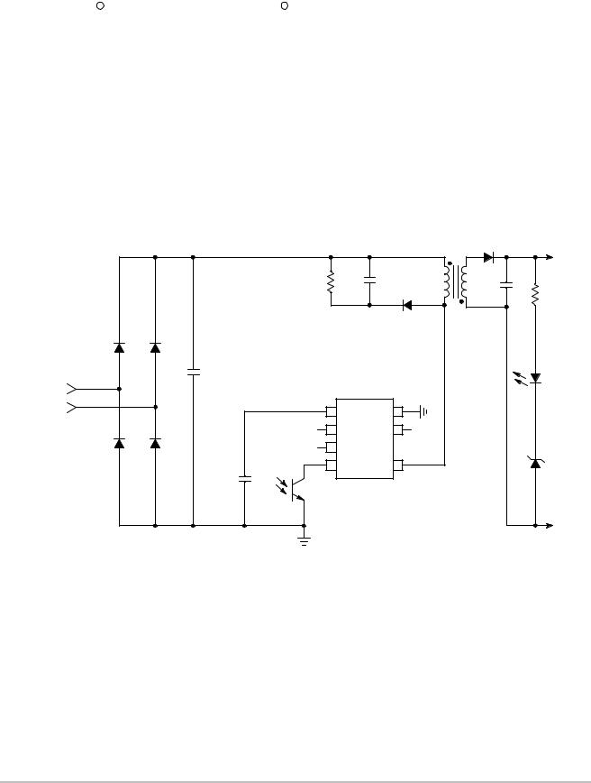
Figure 1. Typical Application Example
Quick Selection Table
|
NCP1010 |
|
NCP1011 |
|
|
NCP1012 |
NCP1013 |
NCP1014 |
||||||||||
|
|
|
|
|
|
|
|
|
|
|
|
|
|
|
|
|
|
|
RDSon [ ] |
|
|
|
22 |
|
|
|
|
|
|
|
11 |
|
|
|
|
||
Ipeak [mA] |
100 |
|
|
250 |
|
|
|
250 |
|
350 |
|
|
450 |
|
||||
|
|
|
|
|
|
|
|
|
|
|
|
|
|
|
|
|
|
|
Freq [kHz] |
65 |
100 |
130 |
|
65 |
100 |
|
130 |
65 |
|
100 |
130 |
65 |
100 |
130 |
65 |
|
100 |
|
|
|
|
|
|
|
|
|
|
|
|
|
|
|
|
|
|
|
http://onsemi.com
2
NCP1010, NCP1011, NCP1012, NCP1013, NCP1014
PIN FUNCTION DESCRIPTION
|
Pin No. |
|
|
|
Pin No. |
(PDIP−7, |
|
|
|
(SOT−223) |
PDIP−7/Gull Wing) |
Pin Name |
Function |
Description |
|
|
|
|
|
1 |
1 |
VCC |
Powers the Internal Circuitry |
This pin is connected to an external capacitor of typi- |
|
|
|
|
cally 10 F. The natural ripple superimposed on the |
|
|
|
|
VCC participates to the frequency jittering. For im- |
|
|
|
|
proved standby performance, an auxiliary VCC can be |
|
|
|
|
connected to Pin 1. The VCC also includes an active |
|
|
|
|
shunt which serves as an opto fail−safe protection. |
|
|
|
|
|
− |
2 |
NC |
− |
− |
|
|
|
|
|
− |
3 |
NC |
− |
− |
|
|
|
|
|
2 |
4 |
FB |
Feedback Signal Input |
By connecting an optocoupler to this pin, the peak |
|
|
|
|
current setpoint is adjusted accordingly to the output |
|
|
|
|
power demand. |
|
|
|
|
|
3 |
5 |
Drain |
Drain Connection |
The internal drain MOSFET connection. |
|
|
|
|
|
− |
− |
− |
− |
− |
|
|
|
|
|
− |
7 |
NC |
− |
This unconnected pin ensures adequate creepage |
|
|
|
|
distance. |
|
|
|
|
|
4 |
8 |
GND |
The IC Ground |
− |
|
|
|
|
|
VCC |
Startup Source |
|
Iref = 7.4 mA − |
VCC |
1 |
|
|
Drain |
IVCC |
|
+ |
|
|
8 |
GND |
|
|
|
|
|
|
|
|
|
|
||
|
Vclamp* |
|
|
|
|
|
|
Rsense |
|
|
|
|
|
|
|
|
|
|
|
|
|
|
|
|
|
I? |
UVLO |
High when VCC 3 V |
S |
|
|
|
|
||
|
IVCC |
|
|
|
R |
|
250 ns |
|
|
||
|
Management |
|
|
|
|
|
|
||||
|
|
|
|
|
|
Q |
|
L.E.B. |
|
|
|
|
|
|
|
|
|
|
|
|
|
||
NC |
2 |
|
|
|
|
|
Reset |
|
|
7 |
NC |
|
EMI Jittering |
|
65, 100 or |
Set |
|
Q |
|
||||
|
4 V |
|
|
Flip−Flop |
|
|
|
||||
|
|
|
130 kHz |
|
|
Driver |
|
|
|||
|
|
|
|
|
|
DCmax = 65% |
|
|
|
||
|
|
|
|
|
Clock |
|
|
|
|
|
|
|
|
|
|
|
|
|
|
|
|
|
|
|
|
|
|
|
|
|
Reset |
|
|
|
|
|
|
18 k |
|
|
|
|
|
|
VCC |
|
|
|
|
|
Error flag armed? |
|
|
|
|
|
|
|
|
NC |
3 |
|
|
|
|
− |
|
|
|
|
|
|
|
|
|
|
+ − |
+ |
|
|
|
|
|
|
|
|
|
|
0.5 V |
|
|
|
|
|
|
|
|
|
Overload? |
|
|
|
|
+ |
|
|
|
|
|
|
|
|
|
|
- |
|
|
||
|
|
|
|
|
|
|
Startup Sequence |
|
|
||
|
|
|
|
|
|
|
|
|
|
||
|
|
|
|
|
Soft−Start |
Overload |
|
|
|
|
|
FB |
4 |
|
|
|
|
|
|
|
Drain |
5 |
Drain |
|
*Vclamp = VCCOFF + 200 mV (8.7 V Typical) |
|
|
|
|
|
|
|
|||
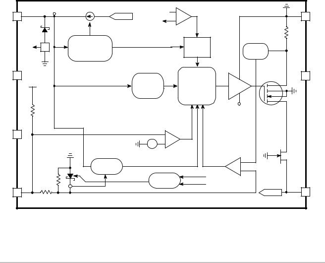
Figure 2. Simplified Internal Circuit Architecture
http://onsemi.com
3

NCP1010, NCP1011, NCP1012, NCP1013, NCP1014
MAXIMUM RATINGS
Rating |
Symbol |
Value |
Unit |
|
|
|
|
Power Supply Voltage on all pins, except Pin 5 (Drain) |
VCC |
−0.3 to 10 |
V |
Drain Voltage |
− |
−0.3 to 700 |
V |
|
|
|
|
Drain Current Peak during Transformer Saturation |
IDS(pk) |
2 x Ilim max |
A |
Maximum Current into Pin 1 when Activating the 8.7 V Active Clamp |
I_VCC |
15 |
mA |
Thermal Characteristics |
|
|
°C/W |
P Suffix, Case 626A and PL Suffix (Gull Wing), Case 626AA |
|
|
|
Junction−to−Lead |
R JL |
9.0 |
|
Junction−to−Air, 2.0 oz Printed Circuit Copper Clad |
R JA |
77 |
|
0.36 Sq. Inch |
|
|
|
1.0 Sq. Inch |
|
60 |
|
ST Suffix, Plastic Package Case 318E |
|
|
|
Junction−to−Lead |
R JL |
14 |
|
Junction−to−Air, 2.0 oz Printed Circuit Copper Clad |
R JA |
74 |
|
0.36 Sq. Inch |
|
|
|
1.0 Sq. Inch |
|
55 |
|
|
|
|
|
Maximum Junction Temperature |
TJmax |
150 |
°C |
Storage Temperature Range |
− |
−60 to +150 |
°C |
|
|
|
|
ESD Capability, Human Body Model (All pins except HV) |
− |
2.0 |
kV |
|
|
|
|
ESD Capability, Machine Model |
− |
200 |
V |
|
|
|
|
Maximum ratings are those values beyond which device damage can occur. Maximum ratings applied to the device are individual stress limit values (not normal operating conditions) and are not valid simultaneously. If these limits are exceeded, device functional operation is not implied, damage may occur and reliability may be affected.
http://onsemi.com
4

NCP1010, NCP1011, NCP1012, NCP1013, NCP1014
ELECTRICAL CHARACTERISTICS (For typical values TJ = 25°C, for min/max values TJ = 0°C to +125°C, Max TJ = 150°C, VCC = 8.0 V unless otherwise noted.)
Rating |
Pin |
Symbol |
Min |
Typ |
Max |
Unit |
|
|
|
|
|
|
|
SUPPLY SECTION AND VCC MANAGEMENT |
|
|
|
|
|
|
VCC Increasing Level at which the Current Source Turns−off |
1 |
VCCOFF |
7.9 |
8.5 |
9.1 |
V |
VCC Decreasing Level at which the Current Source Turns−on |
1 |
VCCON |
6.9 |
7.5 |
8.1 |
V |
VCC Decreasing Level at which the Latch−off Phase Ends |
1 |
VCClatch |
4.4 |
4.7 |
5.1 |
V |
VCC Decreasing Level at which the Internal Latch is Released |
1 |
VCCreset |
− |
3.0 |
− |
V |
Internal IC Consumption, MOSFET Switching at 65 kHz |
1 |
ICC1 |
− |
0.92 |
1.1 |
mA |
|
|
|
|
|
(Note 2) |
|
|
|
|
|
|
|
|
Internal IC Consumption, MOSFET Switching at 100 kHz |
1 |
ICC1 |
− |
0.95 |
1.15 |
mA |
|
|
|
|
|
(Note 2) |
|
|
|
|
|
|
|
|
Internal IC Consumption, MOSFET Switching at 130 kHz |
1 |
ICC1 |
− |
0.98 |
1.2 |
mA |
|
|
|
|
|
(Note 2) |
|
|
|
|
|
|
|
|
Internal IC Consumption, Latch−off Phase, V CC = 6.0 V |
1 |
ICC2 |
− |
290 |
− |
A |
Active Zener Voltage Positive Offset to VCCOFF |
1 |
Vclamp |
140 |
200 |
300 |
mV |
Latch−off Current |
1 |
ILatch |
|
|
|
mA |
NCP1012/13/14 |
|
|
6.3 |
7.4 |
9.2 |
|
NCP1010/11 |
|
|
5.8 |
7.3 |
9.0 |
|
|
|
|
|
|
|
|
POWER SWITCH CIRCUIT |
|
|
|
|
|
|
|
|
|
|
|
|
|
Power Switch Circuit On−state Resistance |
5 |
RDSon |
− |
|
|
|
NCP1012/13/14 (Id = 50 mA) |
|
|
|
|
|
|
TJ = 25°C |
|
|
|
11 |
16 |
|
TJ = 125°C |
|
|
|
19 |
24 |
|
NCP1010/11 (Id = 50 mA) |
|
|
|
|
|
|
TJ = 25°C |
|
|
|
22 |
35 |
|
TJ = 125°C |
|
|
|
38 |
50 |
|
Power Switch Circuit and Startup Breakdown Voltage |
5 |
BVdss |
700 |
− |
− |
V |
(ID(off) = 120 A, TJ = 25°C) |
|
|
|
|
|
|
Power Switch and Startup Breakdown Voltage Off−state |
|
IDS(OFF) |
|
|
|
A |
Leakage Current |
|
|
|
|
|
|
TJ = 25°C (Vds = 700 V) |
5 |
|
− |
50 |
− |
|
TJ = 125°C (Vds = 700 V) |
5 |
|
− |
30 |
− |
|
|
|
|
|
|
|
|
Switching Characteristics |
|
|
|
|
|
ns |
(RL = 50 , Vds Set for Idrain = 0.7 x Ilim) |
|
|
|
|
|
|
Turn−on Time (90%−10%) |
5 |
ton |
− |
20 |
− |
|
Turn−off Time (10%−90%) |
toff |
− |
10 |
− |
|
|
5 |
|
|||||
|
|
|
|
|
|
|
|
|
|
|
|
|
|
INTERNAL STARTUP CURRENT SOURCE |
|
|
|
|
|
|
|
|
|
|
|
|
|
High−voltage Current Source, V CC = 8.0 V |
1 |
IC1 |
|
|
|
mA |
NCP1012/13/14 |
|
|
5.0 |
8.0 |
10 |
|
NCP1010/11 |
|
|
5.0 |
8.5 |
10.3 |
|
|
|
|
|
|
|
|
High−voltage Current Source, V CC = 0 |
1 |
IC2 |
− |
10 |
− |
mA |
CURRENT COMPARATOR TJ = 25°C (Note 2) |
|
|
|
|
|
|
Maximum Internal Current Setpoint, NCP1010 (Note 3) |
5 |
Ipeak (22) |
90 |
100 |
110 |
mA |
|
|
|
|
|
|
|
Maximum Internal Current Setpoint, NCP1011 (Note 3) |
5 |
Ipeak (22) |
225 |
250 |
275 |
mA |
|
|
|
|
|
|
|
Maximum Internal Current Setpoint, NCP1012 (Note 3) |
5 |
Ipeak (11) |
225 |
250 |
275 |
mA |
|
|
|
|
|
|
|
Maximum Internal Current Setpoint, NCP1013 (Note 3) |
5 |
Ipeak (11) |
315 |
350 |
385 |
mA |
|
|
|
|
|
|
|
Maximum Internal Current Setpoint, NCP1014 (Note 3) |
5 |
Ipeak (11) |
405 |
450 |
495 |
mA |
|
|
|
|
|
|
|
Default Internal Current Setpoint for Skip−Cycle Operation, |
− |
ILskip |
− |
25 |
− |
% |
Percentage of Max Ip |
|
|
|
|
|
|
|
|
|
|
|
|
|
Propagation Delay from Current Detection to Drain OFF State |
− |
TDEL |
− |
125 |
− |
ns |
Leading Edge Blanking Duration |
− |
TLEB |
− |
250 |
− |
ns |
2. See characterization curves for temperature evolution. |
|
|
|
|
|
|
3. Adjust di/dt to reach Ipeak in 3.2 sec. |
|
|
|
|
|
|
http://onsemi.com
5

NCP1010, NCP1011, NCP1012, NCP1013, NCP1014
ELECTRICAL CHARACTERISTICS (continued) (For typical values TJ = 25°C, for min/max values TJ = 0°C to +125°C, Max TJ = 150°C, VCC= 8.0 V unless otherwise noted.)
Rating |
Pin |
Symbol |
Min |
Typ |
Max |
Unit |
|
|
|
|
|
|
|
INTERNAL OSCILLATOR |
|
|
|
|
|
|
|
|
|
|
|
|
|
Oscillation Frequency, 65 kHz Version, TJ = 25°C (Note 4) |
− |
fOSC |
59 |
65 |
71 |
kHz |
Oscillation Frequency, 100 kHz Version, TJ = 25°C (Note 4) |
− |
fOSC |
90 |
100 |
110 |
kHz |
Oscillation Frequency, 130 kHz Version, TJ = 25°C (Note 4) |
− |
fOSC |
117 |
130 |
143 |
kHz |
Frequency Dithering Compared to Switching Frequency |
− |
fdither |
− |
3.3 |
− |
% |
(with active DSS) |
|
|
|
|
|
|
|
|
|
|
|
|
|
Maximum Duty−cycle |
− |
Dmax |
62 |
67 |
72 |
% |
|
|
|
|
|
|
|
FEEDBACK SECTION |
|
|
|
|
|
|
|
|
|
|
|
|
|
Internal Pull−up Resistor |
4 |
Rup |
− |
18 |
− |
k |
|
|
|
|
|
|
|
Internal Soft−Start (Guaranteed by Design) |
− |
Tss |
− |
1.0 |
− |
ms |
|
|
|
|
|
|
|
SKIP−CYCLE GENERATION |
|
|
|
|
|
|
|
|
|
|
|
|
|
Default Skip Mode Level on FB Pin |
4 |
Vskip |
− |
0.5 |
− |
V |
|
|
|
|
|
|
|
TEMPERATURE MANAGEMENT |
|
|
|
|
|
|
|
|
|
|
|
|
|
Temperature Shutdown |
− |
TSD |
− |
150 |
− |
°C |
|
|
|
|
|
|
|
Hysteresis in Shutdown |
− |
− |
− |
50 |
− |
°C |
|
|
|
|
|
|
|
4. See characterization curves for temperature evolution.
http://onsemi.com
6

|
|
|
|
NCP1010, NCP1011, NCP1012, NCP1013, NCP1014 |
|
|
|
|||||||
|
|
|
|
|
|
TYPICAL CHARACTERISTICS |
|
|
|
|
|
|||
|
−2.0 |
|
|
|
|
|
|
1.50 |
|
|
|
|
|
|
|
−3.0 |
|
|
|
|
|
|
1.40 |
|
|
|
|
|
|
|
|
|
|
|
|
|
|
|
|
|
|
|
|
|
|
−4.0 |
|
|
|
|
|
|
1.30 |
|
|
|
|
|
|
|
|
|
|
|
|
|
1.20 |
|
|
|
|
|
|
|
|
|
|
|
|
|
|
|
|
|
|
|
|
|
|
( mA) |
−5.0 |
|
|
|
|
|
(mA) |
1.10 |
|
|
|
|
|
|
|
|
|
|
|
|
|
|
|
|
|
|
|||
−6.0 |
|
|
|
|
|
1.00 |
|
|
|
|
|
|
||
IC1 |
−7.0 |
|
|
|
|
|
ICC1 |
0.90 |
|
|
|
|
|
|
|
−8.0 |
|
|
|
|
|
|
0.80 |
|
|
|
|
|
|
|
|
|
|
|
|
|
0.70 |
|
|
|
|
|
|
|
|
|
|
|
|
|
|
|
|
|
|
|
|
|
|
|
−9.0 |
|
|
|
|
|
|
0.60 |
|
|
|
|
|
|
|
|
|
|
|
|
|
|
|
|
|
|
|
|
|
|
−10.0 |
|
|
|
|
|
|
0.50 |
|
|
|
|
|
|
|
−25 |
0 |
25 |
50 |
75 |
100 |
125 |
−25 |
0 |
25 |
50 |
75 |
100 |
125 |
|
|
|
TEMPERATURE (°C) |
|
|
|
|
TEMPERATURE (°C) |
|
|
||||
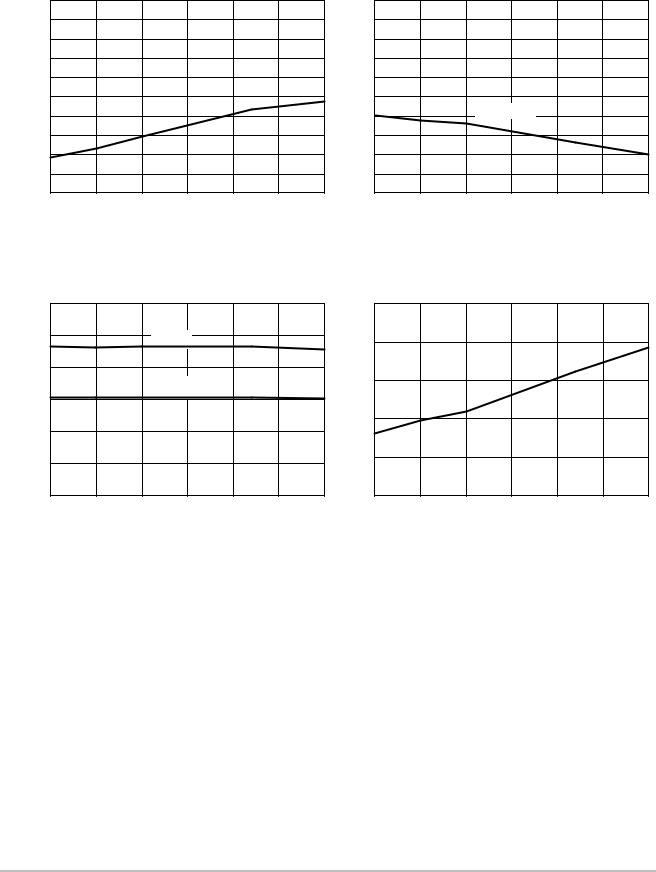
|
|
Figure 3. IC1 @ VCC = 8.0 V, FB = 1.5 V |
|
|
Figure 4. ICC1 @ VCC = 8.0 V, FB = 1.5 V |
|
||||||||
|
|
|
vs. Temperature |
|
|
|
|
vs. Temperature |
|
|
||||
|
0.40 |
|
|
|
|
|
|
9.00 |
|
0.38 |
|
|
|
|
|
|
8.90 |
|
|
|
|
|
|
|
|
|
|
0.36 |
|
|
|
|
|
|
8.80 |
|
0.34 |
|
|
|
|
|
|
|
|
|
|
|
|
|
|
|
|
ICC2 (mA) |
0.32 |
|
|
|
|
|
) |
8.70 |
|
|
|
|
|
VCC−OFF ( V |
|||
|
|
|
|
|
|
|||
0.30 |
|
|
|
|
|
8.60 |
||
0.28 |
|
|
|
|
|
8.50 |
||
|
|
|
|
|
|
|||
0.26 |
|
|
|
|
|
8.40 |
||
|
|
|
|
|
|
|
||
|
0.24 |
|
|
|
|
|
|
|
|
|
|
|
|
|
|
|
|
|
0.22 |
|
|
|
|
|
|
8.30 |
|
|
|
|
|
|
|
|
|
|
0.20 |
|
|
|
|
|
|
8.20 |
|
−25 |
0 |
25 |
50 |
75 |
100 |
125 |
|
−25 |
0 |
25 |
50 |
75 |
100 |
125 |
VCC−ON ( V)
TEMPERATURE (°C) |
TEMPERATURE (°C) |
Figure 5. ICC2 @ VCC = 6.0 V, FB = Open |
Figure 6. VCC OFF, FB = 1.5 V vs. |
|
|
vs. Temperature |
|
|
|
|
|
|
Temperature |
|
|
|
||
8.00 |
|
|
|
|
|
|
|
68 |
|
|
|
|
|
|
7.90 |
|
|
|
|
|
|
|
68 |
|
|
|
|
|
|
7.80 |
|
|
|
|
|
|
|
|
|
|
|
|
|
|
|
|
|
|
|
|
|
|
|
|
|
|
|
|
|
7.70 |
|
|
|
|
|
|
(%) |
67 |
|
|
|
|
|
|
|
|
|
|
|
|
|
|
|
|
|
|
|
||
|
|
|
|
|
|
|
|
|
|
|
|
|
|
|
7.60 |
|
|
|
|
|
|
CYCLE |
|
|
|
|
|
|
|
7.50 |
|
|
|
|
|
|
67 |
|
|
|
|
|
|
|
|
|
|
|
|
|
|
|
|
|
|
|
|
||
7.40 |
|
|
|
|
|
|
DUTY |
66 |
|
|
|
|
|
|
7.30 |
|
|
|
|
|
|
|
|
|
|
|
|
||
|
|
|
|
|
|
|
|
|
|
|
|
|
|
|
7.20 |
|
|
|
|
|
|
|
66 |
|
|
|
|
|
|
|
|
|
|
|
|
|
|
|
|
|
|
|
|
|
7.10 |
|
|
|
|
|
|
|
|
|
|
|
|
|
|
7.00 |
|
|
|
|
|
|
|
65 |
|
|
|
|
|
|
−25 |
0 |
25 |
50 |
75 |
100 |
125 |
|
−25 |
0 |
25 |
50 |
75 |
100 |
125 |
|
|
TEMPERATURE (°C) |
|
|
|
|
|
TEMPERATURE (°C) |
|
|
||||
Figure 7. VCC ON, FB = 3.5 V vs. Temperature |
Figure 8. Duty Cycle vs. Temperature |
http://onsemi.com
7
|
|
|
NCP1010, NCP1011, NCP1012, NCP1013, NCP1014 |
|
|
|
||||||||
|
|
|
|
|
TYPICAL CHARACTERISTICS |
|
|
|
|
|
||||
|
9.00 |
|
|
|
|
|
|
500 |
|
|
|
|
|
|
|
8.80 |
|
|
|
|
|
|
480 |
|
|
|
|
|
|
|
8.60 |
|
|
|
|
|
|
460 |
|
|
|
|
|
|
(mA)LatchI |
8.40 |
|
|
|
|
|
(mA)Ipeak |
440 |
|
|
|
|
|
|
8.20 |
|
|
|
|
|
420 |
|
|
|
|
|
|
||
|
|
|
|
|
|
|
|
|
|
|
|
|
||
|
8.00 |
|
|
|
|
|
|
400 |
|
|
|
|
|
|
|
7.80 |
|
|
|
|
|
|
380 |
|
|
NCP1013 |
|
|
|
|
7.60 |
|
|
|
|
|
|
360 |
|
|
|
|
|
|
|
7.40 |
|
|
|
|
|
|
340 |
|
|
|
|
|
|
|
7.20 |
|
|
|
|
|
|
320 |
|
|
|
|
|
|
|
7.00 |
|
|
|
|
|
|
300 |
|
|
|
|
|
|
|
−25 |
0 |
25 |
50 |
75 |
100 |
125 |
−25 |
0 |
25 |
50 |
75 |
100 |
125 |
|
|
|
TEMPERATURE (°C) |
|
|
|
|
TEMPERATURE (°C) |
|
|
||||
Figure 9. ILatch, FB = 1.5 V vs. Temperature |
Figure 10. Ipeak−RR, V CC = 8.0 V, FB = 3.5 V |
vs. Temperature
fOSC (kHz)
160 |
|
|
|
|
|
|
25.00 |
|
|
|
|
|
|
140 |
|
|
130 kHz |
|
|
|
20.00 |
|
|
|
|
|
|
|
|
|
|
|
|
|
|
|
|
|
|
||
120 |
|
|
|
|
|
|
15.00 |
|
|
|
|
|
|
|
|
|
100 kHz |
|
|
( ) |
|
|
|
|
|
|
|
100 |
|
|
|
|
|
|
|
|
|
|
|
||
|
|
|
|
|
DSon |
|
|
|
|
|
|
|
|
|
|
|
|
|
|
10.00 |
|
|
|
|
|
|
|
80 |
|
|
|
|
|
R |
|
|
|
|
|
|
|
|
|
|
|
|
|
|
|
|
|
|
|
|
|
60 |
|
|
|
|
|
|
5.00 |
|
|
|
|
|
|
|
|
|
|
|
|
|
|
|
|
|
|
|
|
40 |
|
|
|
|
|
|
0.00 |
|
|
|
|
|
|
−25 |
0 |
25 |
50 |
75 |
100 |
125 |
−25 |
0 |
25 |
50 |
75 |
100 |
12 5 |
|
|
TEMPERATURE (°C) |
|
|
|
|
TEMPERATURE (°C) |
|
|
||||
Figure 11. Frequency vs. Temperature |
Figure 12. ON Resistance vs. Temperature, |
NCP1012/1013
http://onsemi.com
8
 Loading...