ON Semiconductor MJW21191, MJW21191G, MJW21192, MJW21192G Service Manual

MJW21192 (NPN),
MJW21191 (PNP)
Complementary Silicon
Plastic Power Transistors
Specifically designed for power audio output, or high power drivers in audio amplifiers.
•DC Current Gain Specified up to 8.0 A at Temperature
•All On Characteristics at Temperature
•High SOA: 20 A, 18 V, 100 ms
•TO−247AE Package
•Pb−Free Packages are Available*
MAXIMUM RATINGS
|
|
|
MJW21191 |
|
Rating |
Symbol |
MJW21192 |
Unit |
|
|
|
|
|
|
Collector−Emitter Voltage |
VCEO |
150 |
Vdc |
|
Collector−Base Voltage |
VCB |
150 |
Vdc |
|
Emitter−Base Voltage |
VEB |
5.0 |
Vdc |
|
Collector Current − |
Continuous |
IC |
8.0 |
Adc |
− |
Peak |
|
16 |
|
|
|
|
|
|
Base Current |
|
IB |
2.0 |
Adc |
Total Power Dissipation @ TC = 25_C |
PD |
125 |
W |
|
Derate above 25_C |
|
0.65 |
W/_C |
|
Operating and Storage Junction |
TJ, Tstg |
– 65 to |
_C |
|
Temperature Range |
|
+150 |
|
|
|
|
|
|
|
THERMAL CHARACTERISTICS
Characteristic |
Symbol |
Max |
Unit |
|
|
|
|
Thermal Resistance, Junction to Case |
RqJC |
1.0 |
_C/W |
Thermal Resistance, Junction to Ambient |
RqJA |
50 |
_C/W |
Maximum ratings are those values beyond which device damage can occur. Maximum ratings applied to the device are individual stress limit values (not normal operating conditions) and are not valid simultaneously. If these limits are exceeded, device functional operation is not implied, damage may occur and reliability may be affected.
1000 |
|
|
|
|
|
|
|
|
|
|
|
|
|
|
|
|
|
|
|
|
|
|
|
|
|
|
|
|
|
|
|
|
|
|
(pF) |
|
|
|
|
|
|
|
|
|
|
|
|
|
|
|
PNP |
|
|
|
|
|
|
|
|
|
|
|
|
|
|
|
|
|
|
|
|
|
|
|
|
|
|
|
|
|
|
|
|
|
|
|
|
|
|
|
|
|
|
|
|
|
|
|
|
|
|
|
|
|
|
|
|
|
|
|
|
|
|
|
|
|
|
|
|
|
|
|
|
|
|
|
|
|
|
|
|
|
|
|
|
|
|
|
|
100 |
|
|
NPN |
|
|
|
|
|
|
|
|
|
|
|
|
|
|
|
|
|
|
|
|
|
|
|
|
|
|
|
|
|
||
|
|
|
|
|
|
|
|
|
|
|
|
|
|
|
|
|
|
|
|
|
|
|
|
|
|
|
|
|
|
|
||||
CAPACITANCE |
|
|
|
|
|
|
|
|
|
|
|
|
|
|
|
|
|
|
|
|
|
|
|
|
|
|
|
|
|
|
|
|
|
|
10 |
|
|
|
|
|
|
|
|
|
|
|
|
|
|
|
|
|
|
|
|
|
|
|
|
|
|
|
|
|
|
|
|
|
|
|
|
|
|
|
|
|
|
|
|
|
|
|
|
|
|
|
|
|
|
|
|
|
|
|
|
|
|
|
|
|
|
|
||
|
|
|
|
|
|
|
|
|
|
|
|
|
|
|
|
|
|
|
|
|
|
|
|
|
|
|
|
|
|
|
|
|
||
|
|
|
|
|
|
|
|
|
|
|
|
|
|
|
|
|
|
|
|
|
|
|
|
|
|
|
|
|
|
|
|
|
||
C, |
|
|
|
|
|
|
|
|
|
|
|
|
|
|
|
|
|
|
|
|
|
|
|
|
|
|
|
|
|
|
|
|
|
|
1.0 |
|
|
|
|
|
|
|
|
|
|
|
|
|
|
|
|
|
|
|
|
|
|
|
|
|
|
|
|
|
|
|
|
|
|
|
|
|
|
|
|
|
|
|
|
|
|
|
|
|
|
|
|
|
|
|
|
|
|
|
|
|
|
|
|
|
|
|
||
|
|
|
|
|
|
|
|
|
|
|
|
|
|
|
|
|
|
|
|
|
|
|
|
|
|
|
|
|
|
|
|
|
|
|
|
|
|
|
|
|
|
|
|
|
|
|
|
|
|
|
|
|
|
|
|
|
|
|
|
|
|
|
|
|
|
|
|
|
|
|
|
|
|
|
|
|
|
|
|
|
|
|
|
|
|
|
|
|
|
|
|
|
|
|
|
|
|
|
|
|
|
|
|
|
|
|
|
|
|
|
|
|
|
|
|
|
|
|
|
|
|
|
|
|
|
|
|
|
|
|
|
|
|
|
|
|
|
|
|
|
|
|
|
|
|
|
|
|
|
|
|
|
|
|
|
|
|
|
|
|
|
|
|
|
|
|
|
|
|
|
|
|
|
|
|
|
|
|
|
|
|
|
|
|
|
|
|
|
|
|
|
|
|
|
|
|
|
|
|
|
|
|
|
|
|
|
|
|
|
|
1.0 |
10 |
100 |
1000 |
||||||||||||||||||||||||||||||
|
|
|
|
|
|
|
|
|
VR, REVERSE VOLTAGE (V) |
|
|
|
|
|
|
|
|
|
||||||||||||||||
Figure 1. Typical Capacitance @ 25°C
*For additional information on our Pb−Free strategy and soldering details, please download the ON Semiconductor Soldering and Mounting Techniques Reference Manual, SOLDERRM/D.
♥ Semiconductor Components Industries, LLC, 2005 |
1 |
June, 2005 − Rev. 2 |
|
http://onsemi.com
8.0 A
POWER TRANSISTORS COMPLEMENTARY SILICON 150 V, 125 W
TO−247
CASE 340L
STYLE 3
1 2 3
MARKING DIAGRAM
MJW2119x
AYWWG
1 BASE  3 EMITTER
2COLLECTOR
x= 1 or 2
A = Assembly Location
Y = Year
WW = Work Week
G = Pb−Free Package
ORDERING INFORMATION
Device |
Package |
Shipping |
|
|
|
MJW21191 |
TO−247 |
30 Units/Rail |
|
|
|
MJW21191G |
TO−247 |
30 Units/Rail |
|
(Pb−Free) |
|
|
|
|
MJW21192 |
TO−247 |
30 Units/Rail |
|
|
|
MJW21192G |
TO−247 |
30 Units/Rail |
|
(Pb−Free) |
|
|
|
|
Publication Order Number:
MJW21192/D

MJW21192 (NPN), MJW21191 (PNP)
ELECTRICAL CHARACTERISTICS (TC = 25_C unless otherwise noted)
Characteristic |
Symbol |
Min |
Max |
Unit |
|
|
|
|
|
OFF CHARACTERISTICS |
|
|
|
|
|
|
|
|
|
Collector−Emitter Sustaining Voltage (Note 1) |
VCEO(sus) |
|
|
Vdc |
(IC = 10 mAdc, IB = 0) |
|
150 |
− |
|
Collector Cutoff Current |
ICES |
|
|
mAdc |
(VCB = 250 Vdc, IE = 0) |
|
− |
10 |
|
Emitter Cutoff Current |
IEBO |
|
|
mAdc |
(VBE = 5.0 Vdc, IC = 0) |
|
− |
10 |
|
ON CHARACTERISTICS (Note 1) |
|
|
|
|
|
|
|
|
|
DC Current Gain |
hFE |
|
|
− |
(IC = 4.0 Adc, VCE = 2.0 Vdc) |
|
15 |
100 |
|
(IC = 8.0 Adc, VCE = 2.0 Vdc) |
|
5.0 |
− |
|
Collector−Emitter Saturation Voltage |
VCE(sat) |
|
|
Vdc |
(IC = 4.0 Adc, IB = 0.4 Adc) |
|
− |
1.0 |
|
(IC = 8.0 Adc, IB = 1.6 Adc) |
|
− |
2.0 |
|
Base−Emitter On Voltage |
VBE(on) |
− |
2.0 |
Vdc |
(IC = 4.0 Adc, VCE = 2.0 Vdc) |
|
|
|
|
DYNAMIC CHARACTERISTICS |
|
|
|
|
|
|
|
|
|
Current Gain − Bandwidth Product (Note 2) |
fT |
4.0 |
− |
MHz |
(IC = 1.0 Adc, VCE = 10 Vdc, ftest = 1.0 MHz) |
|
|
|
|
1. Pulse Test: Pulse Width v 300 ms, Duty Cycle v 2.0%. |
|
|
|
|
|
||||||
2. |
fT = hfe• ftest. |
|
|
|
|
|
|
|
|
||
|
|
1.0 |
|
|
|
|
|
|
|
|
|
|
|
|
D = 0.5 |
|
|
|
|
|
|
|
DUTY |
|
|
|
|
|
|
|
|
|
|
CYCLE, |
|
|
RESISTANCE (NORMALIZED) |
|
|
|
|
|
|
|
|
P(pk) |
D = t1/t2 |
TRANSIENT THERMAL |
|
0.2 |
|
|
|
|
|
|
|
|
|
|
0.1 |
|
|
|
|
|
|
t1 |
|
||
0.1 |
|
|
|
|
|
|
|
t2 |
|
||
|
0.05 |
|
|
|
|
|
ZθJC(t) = r(t) RθJC |
|
|||
|
|
|
|
|
|
RθJC = 1.65°C/W MAX |
|
||||
|
|
|
|
|
|
|
|
||||
|
|
|
|
|
|
|
D CURVES APPLY FOR POWER |
||||
|
0.02 |
|
|
|
|
|
PULSE TRAIN SHOWN |
|
|||
|
|
|
|
|
|
|
|
|
READ TIME AT t1 |
|
|
|
|
0.01 |
0.01 |
|
|
|
|
|
TJ(pk) − TC = P(pk) ZθJC(t) |
|
|
|
|
|
|
|
|
|
|
|
|
||
|
|
|
|
|
|
|
|
|
|
|
|
|
|
|
0.00001 |
0.0001 |
0.001 |
0.01 |
0.1 |
1.0 |
10 |
100 |
1000 |
t, TIME (s)
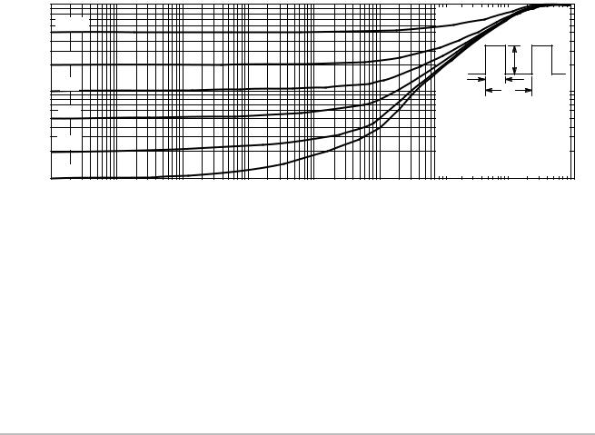
Figure 2. Thermal Response
There are two limitations on the power handling ability of a transistor: average junction temperature and second breakdown. Safe operating area curves indicate IC − VCE limits of the transistor that must be observed for reliable operation, i.e., the transistor must not be subjected to greater dissipation then the curves indicate.
The data of Figures 3 and 4 is based on TJ(pk) = 150_C; TC is variable depending on conditions. Second breakdown
pulse limits are valid for duty cycles to 10% provided TJ(pk) < 150_C. TJ(pk) may be calculated from the data in Figure 2. At high case temperatures, thermal limitations will reduce the power that can be handled to values less than the limitations imposed by second breakdown.
http://onsemi.com
2
 Loading...