


MJE15028
© Semiconductor Components Industries, LLC, 2006
February, 2006 − Rev. 4
1 Publication Order Number:
MJE15028/D
MJE15028, MJE15030 (NPN)
MJE15029, MJE15031 (PNP)
Preferred Device
Complementary Silicon
Plastic Power Transistors
These devices are designed for use as high−frequency drivers in
audio amplifiers.
Features
• DC Current Gain Specified to 4.0 Amperes
h
FE
= 40 (Min) @ I
C
= 3.0 Adc
= 20 (Min) @ I
C
= 4.0 Adc
• Collector−Emitter Sustaining Voltage −
V
CEO(sus)
= 120 Vdc (Min); MJE15028, MJE15029
= 150 Vdc (Min); MJE15030, MJE15031
• High Current Gain − Bandwidth Product
f
T
= 30 MHz (Min) @ I
C
= 500 mAdc
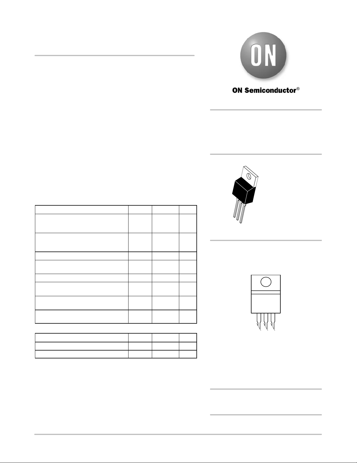
• TO−220AB Compact Package
• Pb−Free Packages are Available*
MAXIMUM RATINGS
Rating Symbol Value Unit
Collector−Emitter Voltage
MJE15028, MJE15029
MJE15030, MJE15031
V
CEO
120
150
Vdc
Collector−Base Voltage
MJE15028, MJE15029
MJE15030, MJE15031
V
CB
120
150
Vdc
Emitter−Base Voltage V
EB
5.0 Vdc
Collector Current − Continuous
− Peak
I
C
I
CM
8.0
16
Adc
Base Current I
B
2.0 Adc
Total Device Dissipation @ T
C
= 25_C
Derate above 25°C
P
D
50
0.40
W
W/_C
Total Device Dissipation @ T
C
= 25_C
Derate above 25°C
P
D
2.0
0.016
W
W/_C
Operating and Storage Junction
Temperature Range
T
J
, T
stg
−65 to
+150
_C
THERMAL CHARACTERISTICS
Characteristics Symbol Max Unit
Thermal Resistance, Junction−to−Case
R
q
JC
2.5
_C/W
Thermal Resistance, Junction−to−Ambient
R
q
JA
62.5
_C/W
Maximum ratings are those values beyond which device damage can occur.
Maximum ratings applied to the device are individual stress limit values (not
normal operating conditions) and are not valid simultaneously. If these limits are
exceeded, device functional operation is not implied, damage may occur and
reliability may be affected.
*For additional information on our Pb−Free strategy and soldering details, please
download the ON Semiconductor Soldering and Mounting Techniques
Reference Manual, SOLDERRM/D.
8 AMPERE
POWER TRANSISTORS
COMPLEMENTARY SILICON
120−150 VOLTS, 50 WATTS
TO−220AB
CASE 221A−09
STYLE 11
http://onsemi.com
MARKING DIAGRAM
2
3
Preferred devices are recommended choices for future use
and best overall value.
MJE150xx = Device Code
x = 28, 29, 30, or 31
G = Pb−Free Package
A = Assembly Location
Y = Year
WW = Work Week
MJE150xxG
AY WW
See detailed ordering and shipping information in the package
dimensions section on page 5 of this data sheet.
ORDERING INFORMATION
MJE15028, MJE15030 (NPN) MJE15029, MJE15031 (PNP)
http://onsemi.com
2
ELECTRICAL CHARACTERISTICS (T
C
= 25_C unless otherwise noted)
Characteristic
Symbol
Min
Max
Unit
OFF CHARACTERISTICS
ООООООООООООООООООО
Î
Collector−Emitter Sustaining Voltage (Note 1)
(I
C
= 10 mAdc, I
B
= 0) MJE15028, MJE15029
MJE15030, MJE15031
ÎÎÎ
Î
V
CEO(sus)
ÎÎ
Î
120
150
Î
Î
−
−
ÎÎ
Î
Vdc
ООООООООООООООООООО
Î
ООООООООООООООООООО
Î
Collector Cutoff Current
(V
CE
= 120 Vdc, I
B
= 0) MJE15028, MJE15029
(V
CE
= 150 Vdc, I
B
= 0) MJE15030, MJE15031
ÎÎÎ
Î
ÎÎÎ
Î
I
CEO
ÎÎ
Î
ÎÎ
Î
−
−
Î
Î
Î
Î
0.1
0.1
ÎÎ
Î
ÎÎ
Î
mAdc
ООООООООООООООООООО
Î
Collector Cutoff Current
(V
CB
= 120 Vdc, I
E
= 0) MJE15028, MJE15029
(V
CB
= 150 Vdc, I
E
= 0) MJE15030, MJE15031
ÎÎÎ
Î
I
CBO
ÎÎ
Î
−
−
Î
Î
10
10
ÎÎ
Î
mAdc
ООООООООООООООООООО
Î
Emitter Cutoff Current
(V
BE
= 5.0 Vdc, I
C
= 0)
ÎÎÎ
Î
I
EBO
ÎÎ
Î
−
Î
Î
10
ÎÎ
Î
mAdc
ON CHARACTERISTICS (Note 1)
ООООООООООООООООООО
Î
ООООООООООООООООООО
Î
ООООООООООООООООООО
Î
DC Current Gain
(I
C
= 0.1 Adc, V
CE
= 2.0 Vdc)
(I
C
= 2.0 Adc, V
CE
= 2.0 Vdc)
(I
C
= 3.0 Adc, V
CE
= 2.0 Vdc)
(I
C
= 4.0 Adc, V
CE
= 2.0 Vdc)
ÎÎÎ
Î
ÎÎÎ
Î
ÎÎÎ
Î
h
FE
ÎÎ
Î
ÎÎ
Î
ÎÎ
Î
40
40
40
20
Î
Î
Î
Î
Î
Î
−
−
−
−
ÎÎ
Î
ÎÎ
Î
ÎÎ
Î
−
ООООООООООООООООООО
Î
DC Current Gain Linearity
(V
CE
From 2.0 V to 20 V, I
C
From 0.1 A to 3 A)
(NPN to PNP)
ÎÎÎ
Î
h
FE
ÎÎÎÎ
Î
Typ
2
3
ÎÎ
Î
ООООООООООООООООООО
Î
Collector−Emitter Saturation Voltage
(I
C
= 1.0 Adc, I
B
= 0.1 Adc)
ÎÎÎ
Î
V
CE(sat)
ÎÎ
Î
−
Î
Î
0.5
ÎÎ
Î
Vdc
Base−Emitter On Voltage
(I
C
= 1.0 Adc, V
CE
= 2.0 Vdc)
V
BE(on)
−
1.0
Vdc
DYNAMIC CHARACTERISTICS
ООООООООООООООООООО
Î
Current Gain − Bandwidth Product (Note 2)
(I
C
= 500 mAdc, V
CE
= 10 Vdc, f
test
= 10 MHz)
ÎÎÎ
Î
f
T
ÎÎ
Î
30
Î
Î
−
ÎÎ
Î
MHz
1. Pulse Test: Pulse Width v 300 ms, Duty Cycle v 2.0%.
2. f
T
= ⎪h
fe
⎪• f
test
.
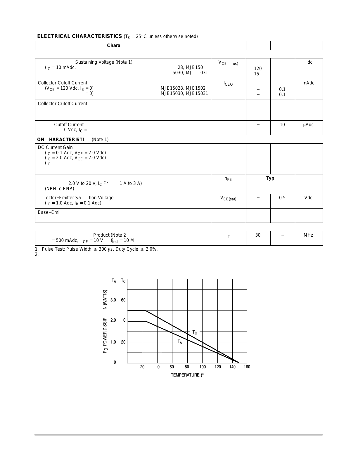
0
Figure 1. Power Derating
T, TEMPERATURE (°C)
0
40 60 100 120 160
40
T
C
20
60
P
D
, POWER DISSIPATION (WATTS)
0
2.0
T
A
1.0
3.0
80 140
T
C
T
A
20
 Loading...