ON Semiconductor MCR218-6FP, MCR218-10FP Technical data

MCR218-10FP
MCR218-6FP, MCR218-10FP
Preferred Device
Silicon Controlled Rectifiers
Reverse Blocking Thyristors
Designed primarily for half-wave ac control applications, such as motor controls, heating controls and power supply crowbar circuits.
•Glass Passivated Junctions with Center Gate Fire for Greater Parameter Uniformity and Stability
•Small, Rugged, Thermowatt Constructed for Low Thermal Resistance, High Heat Dissipation and Durability
•Blocking Voltage to 800 Volts
•80 A Surge Current Capability
•Insulated Package Simplifies Mounting
• Indicates UL Registered Ð File #E69369
• Device Marking: Logo, Device Type, e.g., MCR218±6, Date Code
MAXIMUM RATINGS (TJ = 25°C unless otherwise noted)
Rating |
|
|
Symbol |
Value |
Unit |
|
|
|
|
||
Peak Repetitive Off±State Voltage(1) |
VDRM, |
|
Volts |
||
(TJ = ±40 to +125°C, Sine Wave 50 to |
VRRM |
|
|
||
60 Hz, Gate Open) |
|
|
|
|
|
MCR218±6FP |
|
400 |
|
||
MCR218±10FP |
|
800 |
|
||
|
|
|
|
|
|
On-State RMS Current (T |
C |
= +70°C)(2) |
I |
8.0 |
Amps |
|
|
T(RMS) |
|
|
|
(180° Conduction Angles) |
|
|
|
||
|
|
|
|
||
Peak Nonrepetitive Surge Current |
ITSM |
100 |
Amps |
||
(1/2 Cycle, Sine Wave 60 Hz, |
|
|
|
||
TJ = 125°C) |
|
|
|
|
|
Circuit Fusing (t = 8.3 ms) |
|
I2t |
26 |
A2s |
|
Forward Peak Gate Power |
|
PGM |
5.0 |
Watts |
|
(TC = +70°C, Pulse Width v 1.0 μs) |
|
|
|
||
Forward Average Gate Power |
PG(AV) |
0.5 |
Watt |
||
(TC = +70°C, t = 8.3 ms) |
|
|
|
|
|
Forward Peak Gate Current |
|
IGM |
2.0 |
Amps |
|
(TC = +70°C, Pulse Width v 1.0 μs) |
|
|
|
||
RMS Isolation Voltage (TA = 25°C, |
V(ISO) |
1500 |
Volts |
||
Relative Humidity p 20%) ( ) |
|
|
|
||
|
|
|
|
||
Operating Junction Temperature |
TJ |
±40 to |
°C |
||
|
|
|
|
+125 |
|
|
|
|
|
||
Storage Temperature Range |
Tstg |
±40 to |
°C |
||
|
|
|
|
+150 |
|
|
|
|
|
|
|
(1)VDRM and VRRM for all types can be applied on a continuous basis. Ratings apply for zero or negative gate voltage; however, positive gate voltage shall not be applied concurrent with negative potential on the anode. Blocking voltages shall not be tested with a constant current source such that the voltage ratings of the devices are exceeded.
(2)The case temperature reference point for all TC measurements is a point on the center lead of the package as close as possible to the plastic body.
http://onsemi.com
ISOLATED SCRs ( ) 8 AMPERES RMS
400 thru 800 VOLTS
 G
G
A
 K
K
1
2
|
3 |
|
|
ISOLATED TO±220 Full Pack |
|
|
|
CASE 221C |
|
|
STYLE 2 |
|
|
|
|
|
PIN ASSIGNMENT |
|
|
|
1 |
|
Cathode |
|
|
|
2 |
|
Anode |
|
|
|
3 |
|
Gate |
|
|
|
|
|
|
ORDERING INFORMATION
Device |
Package |
Shipping |
|
|
|
MCR218±6FP |
ISOLATED TO220FP |
500/Box |
|
|
|
MCR218±10FP |
ISOLATED TO220FP |
500/Box |
|
|
|
|
|
|
Preferred devices are recommended choices for future use and best overall value.
Semiconductor Components Industries, LLC, 1999 |
1 |
Publication Order Number: |
February, 2000 ± Rev. 2 |
|
MCR218FP/D |

MCR218±6FP, MCR218±10FP
THERMAL CHARACTERISTICS
Characteristic |
|
|
|
Symbol |
|
Max |
|
|
Unit |
|||
|
|
|
|
|
|
|
|
|
|
|
|
|
Thermal Resistance, Junction to Case |
|
|
|
|
RqJC |
2 |
|
|
°C/W |
|||
Thermal Resistance, Case to Sink |
|
|
|
|
RqCS |
|
2.2 (typ) |
|
|
°C/W |
||
Thermal Resistance, Junction to Ambient |
|
|
|
|
RqJA |
60 |
|
|
°C/W |
|||
Maximum Lead Temperature for Soldering Purposes 1/8″ |
from Case for 10 Seconds |
|
TL |
260 |
|
|
|
°C |
||||
ELECTRICAL CHARACTERISTICS (TC = 25°C unless otherwise noted.) |
|
|
|
|
|
|
|
|
||||
Characteristic |
|
|
Symbol |
|
Min |
|
Typ |
Max |
|
Unit |
||
|
|
|
|
|
|
|
|
|
|
|
|
|
OFF CHARACTERISTICS |
|
|
|
|
|
|
|
|
|
|
|
|
|
|
|
|
|
|
|
|
|
|
|
||
Peak Repetitive Forward or Reverse Blocking Current |
|
IDRM, |
|
|
|
|
|
|
|
|
||
(VD = Rated VDRM, Gate Open) |
TJ = 25°C |
|
IRRM |
|
Ð |
|
Ð |
10 |
|
mA |
||
|
TJ = 125°C |
|
|
|
|
Ð |
|
Ð |
2 |
|
mA |
|
ON CHARACTERISTICS |
|
|
|
|
|
|
|
|
|
|
|
|
|
|
|
|
|
|
|
|
|
||||
Peak Forward On±State Voltage(1) |
|
|
VTM |
|
Ð |
|
1 |
1.8 |
|
Volts |
||
(ITM = 16 A Peak) |
|
|
|
|
|
|
|
|
|
|
|
|
Gate Trigger Current (Continuous dc) |
|
|
IGT |
|
Ð |
|
10 |
25 |
|
mA |
||
(VAK = 12 Vdc, RL = 100 Ohms) |
|
|
|
|
|
|
|
|
|
|
|
|
Gate Trigger Voltage (Continuous dc) |
|
|
VGT |
|
Ð |
|
Ð |
1.5 |
|
Volts |
||
(VAK = 12 Vdc, RL = 100 Ohms) |
|
|
|
|
|
|
|
|
|
|
|
|
Gate Non-Trigger Voltage |
|
|
VGD |
|
0.2 |
|
Ð |
Ð |
|
Volts |
||
(VAK = 12 Vdc, RL = 100 Ohms, TJ = 125°C) |
|
|
|
|
|
|
|
|
|
|
|
|
Holding Current |
|
|
IH |
|
Ð |
|
16 |
30 |
|
mA |
||
(VAK = 12 Vdc, Initiating Current = 200 mA, Gate Open) |
|
|
|
|
|
|
|
|
|
|||
Turn-On Time |
|
|
tgt |
|
Ð |
|
1.5 |
Ð |
|
ms |
||
(ITM = 8 A, IGT = 40 mAdc) |
|
|
|
|
|
|
|
|
|
|
|
|
Turn-Off Time (VD = Rated VDRM, |
TJ = 25°C |
|
tq |
|
|
|
|
|
|
|
ms |
|
ITM = 8 A, IR = 8 A) |
|
|
|
|
Ð |
|
15 |
Ð |
|
|
||
|
TJ = 125°C |
|
|
|
|
Ð |
|
35 |
Ð |
|
|
|
DYNAMIC CHARACTERISTICS |
|
|
|
|
|
|
|
|
|
|
|
|
|
|
|
|
|
|
|
|
|
||||
Critical Rate-of-Rise of Off-State Voltage |
|
|
dv/dt |
|
Ð |
|
100 |
Ð |
|
V/ms |
||
(Gate Open, VD = Rated VDRM, Exponential Waveform) |
|
|
|
|
|
|
|
|
|
|||
(1) Pulse Test: Pulse Width = 1 ms, Duty Cycle p 2%.
http://onsemi.com
2

MCR218±6FP, MCR218±10FP
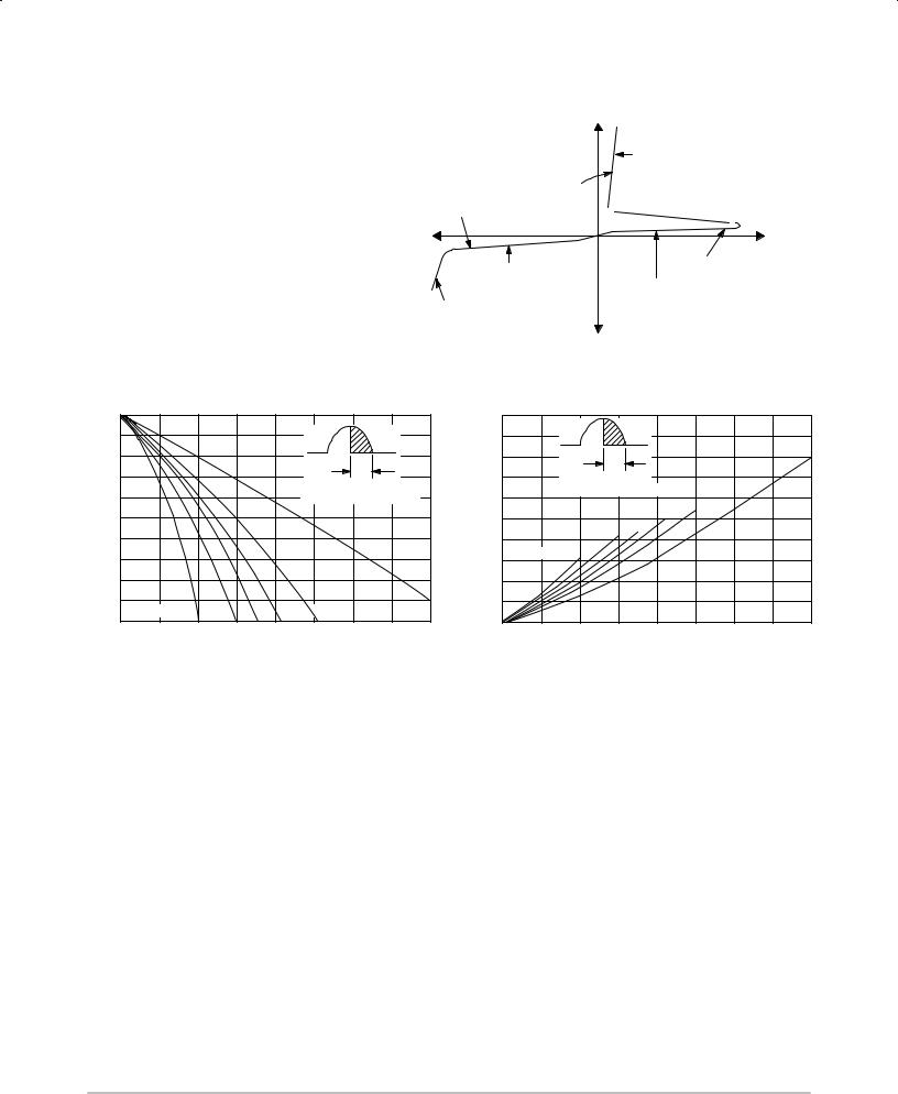
Voltage Current Characteristic of SCR
Symbol |
Parameter |
|
|
VDRM |
Peak Repetitive Off State Forward Voltage |
IDRM |
Peak Forward Blocking Current |
VRRM |
Peak Repetitive Off State Reverse Voltage |
IRRM |
Peak Reverse Blocking Current |
VTM |
Peak on State Voltage |
IH |
Holding Current |
+ Current
Anode +
|
VTM |
on state |
|
IRRM at VRRM |
IH |
|
+ Voltage |
Reverse Blocking Region |
IDRM at VDRM |
(off state) |
Forward Blocking Region |
|
|
Reverse Avalanche Region |
(off state) |
|
|
Anode ± |
|
C) |
|
|
|
|
|
|
|
|
|
|
|
|
|
° |
|
|
|
|
|
|
|
|
|
|
AVERAGE ON-STATE POWER DISSIPATION |
|
|
ALLOWABLE CASE TEMPERATURE ( |
125 |
|
|
|
|
|
|
|
|
|
|
15 |
|
115 |
|
|
|
|
|
|
|
|
|
|
12 |
||
|
|
|
|
|
|
|
|
a |
|
|
|
||
105 |
|
|
|
|
|
α = CONDUCTION ANGLE |
|
(WATTS) |
9 |
||||
|
|
|
|
|
|
|
|
|
|||||
95 |
|
|
|
|
|
|
|
|
|
6 |
|||
85 |
|
|
|
|
|
|
|
dc |
|
|
|||
|
|
|
|
|
|
|
|
|
3 |
||||
|
|
|
|
|
|
|
|
|
|
|
|||
MAXIMUM, |
|
α = 30° |
|
60° |
90° |
120° |
180° |
|
|
|
, |
|
|
75 |
|
|
|
|
(AV) |
|
0 |
||||||
|
|
|
|
|
|
|
|
|
|
||||
C |
0 |
1 |
2 |
3 |
|
4 |
5 |
6 |
7 |
8 |
P |
|
|
T |
|
|
|
||||||||||
|
|
IT(AV), AVERAGE ON-STATE FORWARD CURRENT (AMPS) |
|
|
|
|
|||||||
a |
|
|
α = CONDUCTION ANGLE |
dc |
|
|
120° |
180° |
|
|
|
60° |
90° |
|
|
|
|
α = 30° |
|
|
0 |
1 |
2 |
3 |
4 |
5 |
6 |
7 |
8 |
|
|
IT(AV), AVG. ON-STATE CURRENT (AMPS) |
|
|
||||
Figure 1. Current Derating |
Figure 2. On-State Power Dissipation |
http://onsemi.com
3
 Loading...