


ON Semiconductor LM339, LM239, LM2901, LM2901V, NCV2901 Technical data
...
!
LM339, LM239, LM2901, LM2901V, NCV2901, MC3302
Single Supply Quad
Comparators
These comparators are designed for use in level detection, low−level sensing and memory applications in consumer, automotive, and industrial electronic applications.
Features
•Single or Split Supply Operation
•Low Input Bias Current: 25 nA (Typ)
•Low Input Offset Current: ±5.0 nA (Typ)
•Low Input Offset Voltage
•Input Common Mode Voltage Range to GND
•Low Output Saturation Voltage: 130 mV (Typ) @ 4.0 mA
•TTL and CMOS Compatible
•ESD Clamps on the Inputs Increase Reliability without Affecting Device Operation
•NCV Prefix for Automotive and Other Applications Requiring Site and Control Changes
•Pb−Free Packages are Available
|
http://onsemi.com |
|
SOIC−14 |
14 |
D SUFFIX |
CASE 751A
1
PDIP−14
N, P SUFFIX
CASE 646
14
1
 TSSOP−14 14
  DTB SUFFIX
CASE 948G
1
PIN CONNECTIONS
Output 2 |
1 |
|
14 |
Output 3 |
Output 1 |
2 |
|
13 |
Output 4 |
V |
3 |
|
12 |
GND |
CC |
|
|
|
|
− Input 1 |
4 |
* |
) 11 |
+ Input 4 |
+ Input 1 |
5 |
)1 |
4 * 10 |
− Input 4 |
− Input 2 |
6 |
* |
) 9 |
+ Input 3 |
|
|
)2 |
3 * |
|
+ Input 2 |
7 |
|
8 |
− Input 3 |
(Top View)
ORDERING INFORMATION
See detailed ordering and shipping information in the package dimensions section on page 6 of this data sheet.
DEVICE MARKING INFORMATION
See general marking information in the device marking section on page 8 of this data sheet.
♥ Semiconductor Components Industries, LLC, 2007 |
1 |
Publication Order Number: |
February, 2007 − Rev. 18 |
|
LM339/D |
LM339, LM239, LM2901, LM2901V, NCV2901, MC3302
MAXIMUM RATINGS
Rating |
Symbol |
Value |
Unit |
|
|
|
|
Power Supply Voltage |
VCC |
+36 or ±18 |
Vdc |
LM239/LM339/LM2901, V |
|
|
|
MC3302 |
|
+30 or ±15 |
|
|
|
|
|
Input Differential Voltage Range |
VIDR |
36 |
Vdc |
LM239/LM339/LM2901, V |
|
|
|
MC3302 |
|
30 |
|
|
|
|
|
Input Common Mode Voltage Range |
VICMR |
−0.3 to VCC |
Vdc |
Output Short Circuit to Ground (Note 1) |
ISC |
Continuous |
|
Power Dissipation @ TA = 25°C |
PD |
1.0 |
W |
Plastic Package |
|
||
° |
1/RqJA |
8.0 |
mW/°C |
Derate above 25 C |
|
|
|
Junction Temperature |
TJ |
150 |
°C |
Operating Ambient Temperature Range |
TA |
−25 to +85 |
°C |
LM239 |
|
|
|
MC3302 |
|
−40 to +85 |
|
|
−40 to +105 |
|
|
LM2901 |
|
|
|
|
−40 to +125 |
|
|
LM2901V, NCV2901 |
|
|
|
|
0 to +70 |
|
|
LM339 |
|
|
|
|
|
|
|
|
|
|
|
Storage Temperature Range |
Tstg |
−65 to +150 |
°C |
ESD Protection at any Pin (Note 2) |
VESD |
1500 |
V |
Human Body Model |
|
|
|
Machine Model |
|
200 |
|
|
|
|
|
|
|
|
|
Stresses exceeding Maximum Ratings may damage the device. Maximum Ratings are stress ratings only. Functional operation above the Recommended Operating Conditions is not implied. Extended exposure to stresses above the Recommended Operating Conditions may affect device reliability.
1.The maximum output current may be as high as 20 mA, independent of the magnitude of VCC. Output short circuits to VCC can cause excessive heating and eventual destruction.
2.VESD rating for NCV/SC devices is: Human Body Model − 2000 V; Machine Model − 200 V.
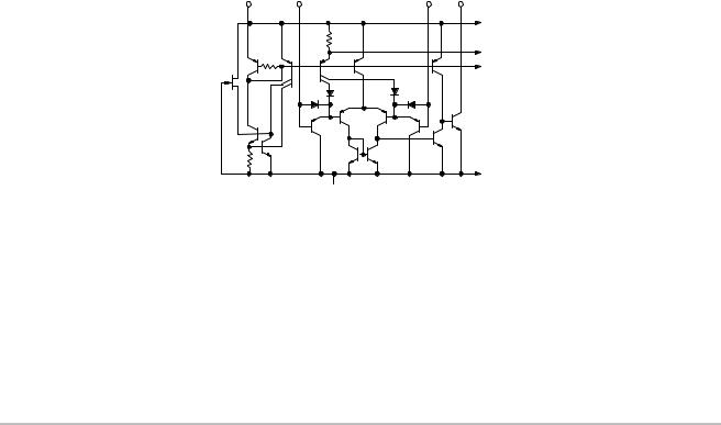
VCC |
+ Input |
− Input |
Output |
 GND
GND
NOTE: Diagram shown is for 1 comparator.
Figure 1. Circuit Schematic
http://onsemi.com
2

LM339, LM239, LM2901, LM2901V, NCV2901, MC3302
ELECTRICAL CHARACTERISTICS (VCC = +5.0 Vdc, TA = +25°C, unless otherwise noted)
|
|
|
|
|
|
|
LM2901/2901V/ |
|
|
|
|
||||
|
|
|
LM239/339 |
|
|
NCV2901 |
|
|
MC3302 |
|
|
||||
|
|
|
|
|
|
|
|
|
|
|
|
|
|
|
|
Characteristic |
Symbol |
Min |
|
Typ |
|
Max |
Min |
|
Typ |
|
Max |
Min |
Typ |
Max |
Unit |
|
|
|
|
|
|
|
|
|
|
|
|
|
|
|
|
Input Offset Voltage (Note 4) |
VIO |
− |
|
±2.0 |
|
±5.0 |
− |
|
±2.0 |
|
±7.0 |
− |
±3.0 |
±20 |
mVdc |
Input Bias Current (Notes 4, 5) |
IIB |
− |
|
25 |
|
250 |
− |
|
25 |
|
250 |
− |
25 |
500 |
nA |
(Output in Analog Range) |
|
|
|
|
|
|
|
|
|
|
|
|
|
|
|
|
|
|
|
|
|
|
|
|
|
|
|
|
|
|
|
Input Offset Current (Note 4) |
IIO |
− |
|
±5.0 |
|
±50 |
− |
|
±5.0 |
|
±50 |
− |
±3.0 |
±100 |
nA |
Input Common Mode Voltage Range |
VICMR |
0 |
|
− |
|
VCC |
0 |
|
− |
|
VCC |
0 |
− |
VCC |
V |
|
|
|
|
|
|
−1.5 |
|
|
|
|
−1.5 |
|
|
−1.5 |
|
|
|
|
|
|
|
|
|
|
|
|
|
|
|
|
|
Supply Current |
ICC |
|
|
|
|
|
|
|
|
|
|
|
|
|
mA |
RL = ∞ (For All Comparators) |
|
− |
|
0.8 |
|
2.0 |
− |
|
0.8 |
|
2.0 |
− |
0.8 |
2.0 |
|
RL = ∞, VCC = 30 Vdc |
|
− |
|
1.0 |
|
2.5 |
− |
|
1.0 |
|
2.5 |
− |
1.0 |
2.5 |
|
|
|
|
|
|
|
|
|
|
|
|
|
|
|
|
|
Voltage Gain |
AVOL |
50 |
|
200 |
|
− |
25 |
|
100 |
|
− |
25 |
100 |
− |
V/mV |
RL ≥ 15 kW, VCC = 15 Vdc |
|
|
|
|
|
|
|
|
|
|
|
|
|
|
|
Large Signal Response Time |
− |
− |
|
300 |
|
− |
− |
|
300 |
|
− |
− |
300 |
− |
ns |
VI = TTL Logic Swing, |
|
|
|
|
|
|
|
|
|
|
|
|
|
|
|
Vref = 1.4 Vdc, VRL = 5.0 Vdc, |
|
|
|
|
|
|
|
|
|
|
|
|
|
|
|
RL = 5.1 kW |
|
|
|
|
|
|
|
|
|
|
|
|
|
|
|
|
|
|
|
|
|
|
|
|
|
|
|
|
|
|
|
Response Time (Note 6) |
− |
− |
|
1.3 |
|
− |
− |
|
1.3 |
|
− |
− |
1.3 |
− |
ms |
VRL = 5.0 Vdc, RL = 5.1 kW |
|
|
|
|
|
|
|
|
|
|
|
|
|
|
|
|
|
|
|
|
|
|
|
|
|
|
|
|
|
|
|
Output Sink Current |
ISink |
6.0 |
|
16 |
|
− |
6.0 |
|
16 |
|
− |
6.0 |
16 |
− |
mA |
VI (−) ≥ +1.0 Vdc, VI(+) = 0, |
|
|
|
|
|
|
|
|
|
|
|
|
|
|
|
VO ≤ 1.5 Vdc |
|
|
|
|
|
|
|
|
|
|
|
|
|
|
|
Saturation Voltage |
Vsat |
− |
|
130 |
|
400 |
− |
|
130 |
|
400 |
− |
130 |
500 |
mV |
VI(−) ≥ +1.0 Vdc, VI(+) = 0, |
|
|
|
|
|
|
|
|
|
|
|
|
|
|
|
Isink ≤ 4.0 mA |
|
|
|
|
|
|
|
|
|
|
|
|
|
|
|
Output Leakage Current |
IOL |
− |
|
0.1 |
|
− |
− |
|
0.1 |
|
− |
− |
0.1 |
− |
nA |
VI(+) ≥ +1.0 Vdc, VI(−) = 0, |
|
|
|
|
|
|
|
|
|
|
|
|
|
|
|
VO = +5.0 Vdc |
|
|
|
|
|
|
|
|
|
|
|
|
|
|
|
3.(LM239) Tlow = −25°C, Thigh = +85° (LM339) Tlow = 0°C, Thigh = +70°C (MC3302) Tlow = −40°C, Thigh = +85°C (LM2901) Tlow = −40°C, Thigh = +105°
(LM2901V & NCV2901) Tlow = −40°C, Thigh = +125°C
NCV2901 is qualified for automotive use.
4.At the output switch point, VO ] 1.4 Vdc, RS ≤ 100 W 5.0 Vdc ≤ VCC ≤ 30 Vdc, with the inputs over the full common mode range (0 Vdc to VCC −1.5 Vdc).
5.The bias current flows out of the inputs due to the PNP input stage. This current is virtually constant, independent of the output state.
6.The response time specified is for a 100 mV input step with 5.0 mV overdrive. For larger signals, 300 ns is typical.
http://onsemi.com
3
LM339, LM239, LM2901, LM2901V, NCV2901, MC3302
PERFORMANCE CHARACTERISTICS (VCC = +5.0 Vdc, TA = Tlow to Thigh [Note 7])
|
|
|
|
|
|
LM2901/2901V/ |
|
|
|
|
|
|
||||
|
|
|
LM239/339 |
|
NCV2901 |
|
|
MC3302 |
|
|
||||||
|
|
|
|
|
|
|
|
|
|
|
|
|
|
|
|
|
Characteristic |
Symbol |
Min |
|
Typ |
Max |
Min |
|
Typ |
|
Max |
Min |
|
Typ |
|
Max |
Unit |
|
|
|
|
|
|
|
|
|
|
|
|
|
|
|
|
|
Input Offset Voltage (Note 8) |
VIO |
− |
|
− |
±9.0 |
− |
|
− |
|
±15 |
− |
|
− |
|
±40 |
mVdc |
Input Bias Current (Notes 8, 9) |
IIB |
− |
|
− |
400 |
− |
|
− |
|
500 |
− |
|
− |
|
1000 |
nA |
(Output in Analog Range) |
|
|
|
|
|
|
|
|
|
|
|
|
|
|
|
|
|
|
|
|
|
|
|
|
|
|
|
|
|
|
|
|
|
Input Offset Current (Note 8) |
IIO |
− |
|
− |
±150 |
− |
|
− |
|
±200 |
− |
|
− |
|
±300 |
nA |
Input Common Mode Voltage Range |
VICMR |
0 |
|
− |
VCC |
0 |
|
− |
|
VCC |
0 |
|
− |
|
VCC |
V |
|
|
|
|
|
−2.0 |
|
|
|
|
−2.0 |
|
|
|
|
−2.0 |
|
|
|
|
|
|
|
|
|
|
|
|
|
|
|
|
|
|
Saturation Voltage |
Vsat |
− |
|
− |
700 |
− |
|
− |
|
700 |
− |
|
− |
|
700 |
mV |
VI(−) ≥ +1.0 Vdc, VI(+) = 0, |
|
|
|
|
|
|
|
|
|
|
|
|
|
|
|
|
Isink ≤ 4.0 mA |
|
|
|
|
|
|
|
|
|
|
|
|
|
|
|
|
Output Leakage Current |
IOL |
− |
|
− |
1.0 |
− |
|
− |
|
1.0 |
− |
|
− |
|
1.0 |
mA |
VI(+) ≥ +1.0 Vdc, VI(−) = 0, |
|
|
|
|
|
|
|
|
|
|
|
|
|
|
|
|
VO = 30 Vdc |
|
|
|
|
|
|
|
|
|
|
|
|
|
|
|
|
Differential Input Voltage |
VID |
− |
|
− |
VCC |
− |
|
− |
|
VCC |
− |
|
− |
|
VCC |
Vdc |
All VI ≥ 0 Vdc |
|
|
|
|
|
|
|
|
|
|
|
|
|
|
|
|
7.(LM239) Tlow = −25°C, Thigh = +85° (LM339) Tlow = 0°C, Thigh = +70°C (MC3302) Tlow = −40°C, Thigh = +85°C (LM2901) Tlow = −40°C, Thigh = +105°
(LM2901V & NCV2901) Tlow = −40°C, Thigh = +125°C
NCV2901 is qualified for automotive use.
8.At the output switch point, VO ] 1.4 Vdc, RS ≤ 100 W 5.0 Vdc ≤ VCC ≤ 30 Vdc, with the inputs over the full common mode range (0 Vdc to VCC −1.5 Vdc).
9.The bias current flows out of the inputs due to the PNP input stage. This current is virtually constant, independent of the output state.
10.The response time specified is for a 100 mV input step with 5.0 mV overdrive. For larger signals, 300 ns is typical.
|
|
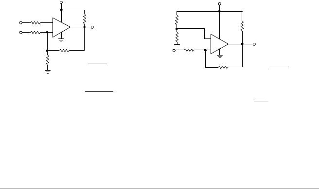
+ VCC |
|
|
|
|
|
+ VCC |
|
|
|
|
|
|
|
R3 |
|
|
|
|
|
|
|
|
|
|
|
|
|
|
10 k |
|
|
|
10 k |
|
|
Rref |
|
|
|
|
|
|
Vin |
|
− |
|
|
|
|
|
|
|
|
|
|
||
Rref |
|
|
VO |
|
Vref |
10 k |
|
|
|
|
|
|||
|
|
|
|
|
|
|
|
|
|
|||||
+ VCC |
+ |
|
|
|
|
|
|
|
|
|
||||
|
|
|
|
|
|
|
|
|
|
|
|
|
||
|
|
|
|
|
|
|
R1 |
|
|
|
|
|
|
|
|
|
|
|
|
|
|
|
− |
|
|
|
|
|
|
|
|
|
R2 |
|
|
|
|
R2 |
+ |
VO |
|
|
|
|
|
Vref |
|
|
|
|
|
|
Vin |
|
|
|
|
|
|
|
|
|
|
|
|
|
|
|
|
|
|
|
||
|
10k |
R1 |
1.0 M |
|
VCC R1 |
|
10 k |
R3 |
|
|
V |
R1 |
|
|
|
|
|
V |
|
[ |
|
|
|
|
|
|
|||
|
|
|
ref |
Rref |
+ R1 |
|
|
|
Vref |
= |
|
CC |
|
|
|
|
|
|
|
|
|
1.0 M |
Rref + R1 |
|
|||||
|
|
|
R3 ] R1 / / Rref / / R2 |
|
|
|
|
|
||||||
|
|
|
|
|
R2 [ R1 / / Rref |
|
|
|||||||
|
|
|
|
|
R1 / / Rref |
|
|
|
|
|||||
|
|
|
VH |
|
[VO(max) − VO(min)] |
|
Amount of Hysteresis VH |
|
||||||
|
|
|
= |
|
|
|
||||||||
|
|
|
|
|
R1/ / Rref + R2 |
|
|
|
R2 |
|
|
|
|
|
|
|
|
|
|
|
|
|
|
VH = |
|
[(VO(max) |
− VO(min)] |
||
|
|
|
R2 Rref / / R1 |
|
|
R2 + R3 |
||||||||
|
|
|
|
|
|
|
|
|
||||||
|
Figure 2. Inverting Comparator |
|
Figure 3. Noninverting Comparator |
|
||||||||||
|
|
with Hysteresis |
|
|
|
with Hysteresis |
|
|
|
|
|
|||
http://onsemi.com
4
 Loading...