


Motorola LM301AN, LM301ADR2, LM301AD, LM201ADR2, LM201AN Datasheet
...
Order this document by LM301A/D
Operational Amplifiers
A general purpose operational amplifier that allows the user to choose the compensation capacitor best suited to his needs. With proper compensation, summing amplifier slew rates to 10 V/μs can be obtained.
•Low Input Offset Current: 20 nA Maximum Over Temperature Range
•External Frequency Compensation for Flexibility
•Class AB Output Provides Excellent Linearity
•Output Short Circuit Protection
•Guaranteed Drift Characteristics
|
Figure 1. Standard |
|
Figure 2. Double±Ended |
||||||
|
Compensation and |
|
Limit Detector |
|
|||||
Offset Balancing Circuit |
|
VCC |
|
|
|
|
|||
|
|
VEE |
|
VUT |
|
|
|
|
|
Inverting |
|
|
+ |
|
|
|
|
||
VCC |
|
|
|
|
|
|
VO |
||
Input |
|
|
|
|
|
|
|
||
Non± |
|
Output |
|
|
|
|
|
|
|
Inverting |
|
|
VI |
VEE |
|
MZ4622 or Equiv. |
|||
Input |
|
|
|
||||||
+ |
|
|
|
|
|
||||
|
|
Balance |
|
VCC |
|
|
|
|
|
|
|
Freq |
|
|
|
3.9 V |
|
||
Balance |
Compen |
|
|
|
|
|
|
|
|
|
|
5.1 MΩ |
|
|
|
|
|
|
|
|
10 MΩ |
30 pF |
|
VLT |
|
|
|
VO |
|
|
|
|
|
|
|
|
|
||
|
|
20 k |
VEE |
|
|
|
VO |
= 4.8 V for |
|
|
|
|
|
|
V |
|
VLT |
≤ VI ≤ VUT |
|
|
|
|
|
|
EE |
VO = ±0.4 V |
|
||
|
|
|
|
|
|
VI < VLT or VI > VUT |
|||
|
|
|
|
|
|
|
|||
|
|
|
|
|
(Pins Not Shown Are Not Connected) |
||||
|
|
Figure 3. Representative Circuit Schematic |
|
|
|||||
|
|
|
Balance |
|
Compensation |
|
VCC |
|
|
|
|
|
|
|
|
|
|
|
|
Inputs |
|
|
|
|
|
|
|
|
|
|
+ |
|
|
|
|
|
|
|
|
|
|
|
|
|
500 |
|
|
25 |
Output |
|
|
|
|
|
|
|
|
||
|
|
|
|
|
|
|
50 |
|
|
|
|
450 |
|
|
|
|
|
|
|
|
|
|
40 k |
|
40 k |
80 k |
|
|
|
5 k |
20 k |
10 k |
|
|
|
1.0 k |
|
|
|
|
250 |
Balance |
|
|
|
|
|
VEE |
|
|
|
|
|
|
|
|
|
||
LM301A
LM201A
OPERATIONAL AMPLIFIERS
SEMICONDUCTOR
TECHNICAL DATA
8
1
N SUFFIX
PLASTIC PACKAGE
CASE 626
8


1
D SUFFIX
PLASTIC PACKAGE
CASE 751
(SO±8)
PIN CONNECTIONS
Balance |
1 |
8 |
Compensation |
|
|
2 |
7 |
V |
|
Inputs |
|
|
CC |
|
3 |
6 |
Output |
||
|
||||
V |
4 |
5 |
Balance |
|
EE |
|
|
|
(Top View)
ORDERING INFORMATION
|
Operating |
|
|
Device |
Temperature Range |
Package |
|
|
|
|
|
LM301AD |
TA = 0° to +70°C |
SO±8 |
|
LM301AN |
Plastic DIP |
||
|
|||
|
|
|
|
LM201AD |
TA = ± 25° to +85°C |
SO±8 |
|
LM201AN |
Plastic DIP |
||
|
|||
|
|
|
Motorola, Inc. 1996 |
Rev 5 |
|
|
LM301A LM201A |
|
||
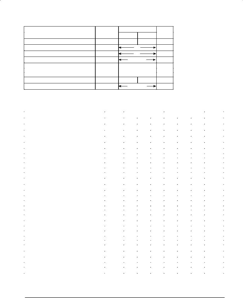
MAXIMUM RATINGS |
|
|
|
|
|
|
|
|
Value |
|
|
Rating |
|
Symbol |
LM201A |
LM301A |
Unit |
Power Supply Voltage |
|
VCC, VEE |
±22 |
±18 |
Vdc |
Input Differential Voltage |
|
VID |
±30 |
|
V |
Input Common Mode Range (Note 1) |
|
VICR |
±15 |
|
V |
Output Short Circuit Duration |
|
tSC |
Continuous |
|
|
Power Dissipation (Package Limitation) |
PD |
|
|
|
|
Plastic Dual±In±Line Package |
(LM201A/ |
|
625 |
625 |
mW |
Derate above TA = +25°C |
301A) |
|
5.0 |
5.0 |
mW/°C |
Operating Ambient Temperature Range |
TA |
±25 to +85 |
0 to +70 |
°C |
|
Storage Temperature Range |
|
Tstg |
± 65 to +150 |
°C |
|
NOTE: 1. For supply voltages less than ±15 V, the absolute maximum input voltage is equal to the supply voltage.
ELECTRICAL CHARACTERISTICS (TA = +25°C, unless otherwise noted.) Unless otherwise specified, these specifications apply for supply voltages from ± 5.0 V to ± 20 V for the LM201A, and from ± 5.0 V to ±15 V for the LM301A.
|
|
|
LM201A |
|
|
LM301A |
|
|
Characteristic |
Symbol |
|
|
|
|
|
|
Unit |
Min |
Typ |
Max |
Min |
Typ |
Max |
|||
|
|
|
|
|
|
|
|
|
Input Offset Voltage (RS ≤ 50 kΩ) |
VIO |
± |
0.7 |
2.0 |
± |
2.0 |
7.5 |
mV |
Input Offset Current |
IIO |
± |
1.5 |
10 |
± |
3.0 |
50 |
nA |
Input Bias Current |
IIB |
± |
30 |
75 |
± |
70 |
250 |
nA |
Input Resistance |
ri |
1.5 |
4.0 |
± |
0.5 |
2.0 |
± |
MΩ |
Supply Current |
ICC,IEE |
|
|
|
|
|
|
mA |
VCC/VEE = ± 20 V |
|
± |
1.8 |
3.0 |
± |
± |
± |
|
VCC/VEE = ±15 V |
|
± |
± |
± |
± |
1.8 |
3.0 |
|
Large Signal Voltage Gain |
AV |
50 |
160 |
± |
25 |
160 |
± |
V/mV |
(VCC/VEE = ±15 V, VO = ±10 V, RL > 2.0 kΩ) |
|
|
|
|
|
|
|
|
The following specifications apply over the operating temperature range.
Input Offset Voltage (RS ≤ 50 kΩ) |
VIO |
|
± |
± |
3.0 |
± |
± |
10 |
mV |
Input Offset Current |
IIO |
|
± |
± |
20 |
± |
± |
70 |
nA |
Avg Temperature Coefficient of Input Offset Voltage |
VIO/ |
T |
± |
3.0 |
15 |
± |
6.0 |
30 |
μV/°C |
TA(min) ≤ TA ≤ TA (max) |
|
|
|
|
|
|
|
|
|
Avg Temperature Coefficient of Input Offset Current |
IIO/ |
T |
|
|
|
|
|
|
nA/°C |
+25°C ≤ TA ≤ TA (max) |
|
|
± |
0.01 |
0.1 |
± |
0.01 |
0.3 |
|
TA(min) ≤ TA ≤ 25°C |
|
|
± |
0.02 |
0.2 |
± |
0.02 |
0.6 |
|
Input Bias Current |
IIB |
|
± |
± |
100 |
± |
± |
300 |
nA |
Large Signal Voltage Gain |
AVOL |
25 |
± |
± |
15 |
± |
± |
V/mV |
|
(VCC/VEE = ±15 V, VO = ±10V, RL > 2.0 kΩ) |
|
|
|
|
|
|
|
|
|
Input Voltage Range |
VICR |
|
|
|
|
|
|
V |
|
VCC/VEE = ± 20 V |
|
|
±15 |
± |
+15 |
± |
± |
± |
|
VCC/VEE = ±15 V |
|
|
± |
± |
± |
±12 |
± |
+12 |
|
Common Mode Rejection (RS ≤ 50 kΩ) |
CMR |
80 |
96 |
± |
70 |
90 |
± |
dB |
|
Supply Voltage Rejection (RS ≤ 50 kΩ) |
PSR |
|
80 |
96 |
± |
70 |
96 |
± |
dB |
Output Voltage Swing |
VO |
|
±12 |
±14 |
± |
±12 |
±14 |
± |
V |
(VCC/VEE = ±15 V, RL = ±10 kΩ, RL > 2.0 kΩ) |
|
|
±10 |
±13 |
± |
±10 |
±13 |
± |
|
Supply Currents (TA = TA(max), VCC/VEE = ± 20 V) |
ICC,IEE |
± |
1.2 |
2.5 |
± |
± |
± |
mA |
|
2 |
MOTOROLA ANALOG IC DEVICE DATA |
 Loading...