


Order this document from L4949/D
Multifunction Very Low
Dropout Voltage Regulator
The L4949 is a monolithic integrated 5.0 V voltage regulator with a very low dropout and additional functions such as power±on reset and input voltage sense.
It is designed for supplying the micro±computer controlled systems especially in automotive applications.
•Operating DC Supply Voltage Range 5.0 V to 28 V
•Transient Supply Voltage Up to 40 V
•Extremely Low Quiescent Current in Standby Mode
•High Precision Standby Output Voltage 5.0 V ±1%
•Output Current Capability Up to 100 mA
•Very Low Dropout Voltage Less Than 0.4 V
•Reset Circuit Sensing The Output Voltage
•Programmable Reset Pulse Delay With External Capacitor
•Voltage Sense Comparator
•Thermal Shutdown and Short Circuit Protections
|
Representative Block Diagram |
||||
|
|
|
Output |
|
|
|
VZ |
Voltage (Vout) |
CT |
|
|
|
3 |
8 |
4 |
||
Supply |
|
|
|
|
|
Voltage (VCC) |
Preregulator |
|
|
|
|
|
|
|
|
|
|
1 |
6.0 V |
|
|
|
|
|
|
|
|
|
|
|
|
|
2.0 μA |
|
Reset |
|
|
|
|
|
|
|
|
|
|
|
6 |
|
|
|
|
|
+ |
|
Regulator |
|
|
|
2.0 V |
|
|
|
|
± |
|
|
Vs |
|
Reset |
|
Sense |
Sense |
|
|
|
Output |
|
Input |
|
|
|
|
(So) |
(Si) |
|
|
|
|
7 |
|
|
|
|
|
|
2 |
|
|
|
|
|
|
|
|
|
|
+ |
|
|
|
|
|
1.23 V |
|
1.23 Vref |
|
|
|
± |
|
|
|
Sense |
|
|
|
|
5 |
Gnd |
|
|
L4949
MULTIFUNCTION
VERY LOW DROPOUT
VOLTAGE REGULATOR
SILICON MONOLITHIC
INTEGRATED CIRCUIT
8
1
N SUFFIX
PLASTIC PACKAGE
CASE 626
8
1
D SUFFIX
PLASTIC PACKAGE
CASE 751
PIN CONNECTIONS
VCC |
|
|
|
|
|
|
Vout |
1 |
|
|
|
|
8 |
||
Si |
|
|
|
|
|
|
So |
2 |
|
|
|
|
7 |
||
VZ |
|
|
|
|
|
|
Reset |
3 |
|
|
|
|
6 |
||
CT |
|
|
|
|
|
|
Gnd |
4 |
|
|
|
|
5 |
||
|
|
|
|
|
|
|
|
|
|
|
(Top View) |
|
|||
|
ORDERING INFORMATION |
||
|
|
Operating |
|
Device |
|
Temperature Range |
Package |
|
|
|
|
L4949N |
|
TJ = ±40° to +125°C |
DIP±8 |
|
|
|
|
L4949D |
|
SO±8 |
|
|
|
||
|
|
|
|
Motorola, Inc. 1998 |
Rev 1 |

L4949
ABSOLUTE MAXIMUM RATINGS (Absolute Maximum Ratings indicate limits beyond which damage to the device may occur.)
Rating |
Symbol |
Value |
Unit |
|
|
|
|
DC Operating Supply Voltage |
VCC |
28 |
V |
Transient Supply Voltage (t < 1.0 s) |
VCC TR |
40 |
V |
Output Current |
Iout |
Internally |
± |
|
|
Limited |
|
|
|
|
|
Output Voltage |
Vout |
20 |
V |
Sense Input Current |
ISI |
±1.0 |
mA |
Sense Input Voltage |
VSI |
VCC |
± |
Output Voltages |
|
|
V |
Reset Output |
VReset |
20 |
|
Sense Output |
VSO |
20 |
|
Output Currents |
|
|
mA |
Reset Output |
IReset |
5.0 |
|
Sense Output |
ISO |
5.0 |
|
Preregulator Output Voltage |
VZ |
7.0 |
V |
Preregulator Output Current |
IZ |
5.0 |
mA |
ESD Protection at any pin |
|
|
V |
|
|
|
|
Human Body Model |
± |
2000 |
|
Machine Model |
± |
400 |
|
|
|
|
|
Thermal Resistance, Junction±to±Air |
RθJA |
|
°C/W |
P Suffix, DIP±8 Plastic Package, Case 626 |
|
100 |
|
D Suffix, SO±8 Plastic Package, Case 751 |
|
200 |
|
|
|
|
|
Maximim Junction Temperature |
TJ |
150 |
°C |
Storage Temperature Range |
Tstg |
±65 to +150 |
°C |
NOTE: ESD data available upon request.
ELECTRICAL CHARACTERISTICS (VCC = 14 V, ±40°C < TJ < 125°C, unless otherwise specified.)
Characteristic |
Symbol |
Min |
Typ |
Max |
Unit |
|
|
|
|
|
|
|
|
Output Voltage (TJ = 25°C, Iout = 1.0 mA) |
Vout |
4.95 |
5.0 |
5.05 |
V |
|
Output Voltage (6.0 V < VCC < 28 V, 1.0 mA < Iout < 50 mA) |
Vout |
4.9 |
5.0 |
5.1 |
V |
|
Output Voltage (VCC = 35 V, t < 1.0 s, 1.0 mA < Iout < 50 mA) |
Vout |
4.9 |
5.0 |
5.1 |
V |
|
Dropout Voltage |
Vdrop |
|
|
|
V |
|
Iout = 10 mA |
|
± |
0.1 |
0.25 |
|
|
Iout = 50 mA |
|
± |
0.2 |
0.40 |
|
|
Iout = 100 mA |
|
± |
0.3 |
0.50 |
|
|
Input to Output Voltage Difference in Undervoltage Condition |
VIO |
± |
0.2 |
0.4 |
V |
|
(VCC = 4.0 V, Iout = 35 mA) |
|
|
|
|
|
|
Line Regulation (6.0 V < VCC < 28 V, Iout = 1.0 mA) |
Regline |
± |
1.0 |
20 |
mV |
|
Load Regulation (1.0 mA < Iout < 100 mA) |
Regload |
± |
8.0 |
30 |
mV |
|
Current Limit |
ILim |
|
|
|
mA |
|
Vout = 4.5 V |
|
105 |
200 |
400 |
|
|
Vout = 0 V |
|
± |
100 |
± |
|
|
Quiescent Current (Iout = 0.3 mA, TJ < 100°C) |
IQSE |
± |
150 |
260 |
μA |
|
Quiescent Current (Iout = 100 mA) |
IQ |
± |
± |
5.0 |
mA |
|
2 |
MOTOROLA ANALOG IC DEVICE DATA |
L4949
ELECTRICAL CHARACTERISTICS (continued) (VCC = 14 V, ±40°C < TJ < 125°C, unless otherwise specified.)
Characteristic |
Symbol |
Min |
Typ |
Max |
Unit |
|
|
|
|
|
|
|
|
RESET |
|
|
|
|
|
|
|
|
|
|
|
|
|
Reset Threshold Voltage |
VResth |
± |
Vout ± 0.5 |
± |
V |
|
Reset Threshold Hysteresis |
VResth,hys |
|
|
|
mV |
|
@ TJ = 25°C |
|
50 |
100 |
200 |
|
|
@ TJ = ±40 to +125°C |
|
50 |
± |
300 |
|
|
Reset Pulse Delay (CT = 100 nF, tR ≥ 100 μs) |
tResD |
55 |
100 |
180 |
ms |
|
Reset Reaction Time (CT = 100 nF) |
tResR |
± |
5.0 |
30 |
μs |
|
Reset Output Low Voltage (RReset = 10 kΩ to Vout, VCC ≥ 3.0 V) |
VResL |
± |
± |
0.4 |
V |
|
Reset Output High Leakage Current (VReset = 5.0 V) |
IResH |
± |
± |
1.0 |
μA |
|
Delay Comparator Threshold |
VCTth |
± |
2.0 |
± |
V |
|
Delay Comparator Threshold Hysteresis |
VCTth, hys |
± |
100 |
± |
mV |
|
SENSE |
|
|
|
|
|
|
|
|
|
|
|
|
|
Sense Low Threshold (VSI Decreasing = 1.5 V to 1.0 V) |
VSOth |
1.16 |
1.23 |
1.35 |
V |
|
Sense Threshold Hysteresis |
VSOth,hys |
20 |
100 |
200 |
mV |
|
Sense Output Low Voltage |
VSOL |
± |
± |
0.4 |
V |
|
(VSI ≤ 1.16 V, VCC ≥ 3.0 V, RSO = 10 kΩ to Vout) |
|
|
|
|
|
|
Sense Output Leakage (VSO = 5.0 V, VSI ≥ 1.5 V) |
ISOH |
± |
± |
1.0 |
μA |
|
Sense Input Current |
ISI |
±1.0 |
0.1 |
1.0 |
μA |
|
PREREGULATOR |
|
|
|
|
|
|
|
|
|
|
|
|
|
Preregulator Output Voltage (IZ = 10 μA) |
VZ |
± |
6.3 |
± |
V |
|
|
|
PIN FUNCTION DESCRIPTION |
|
|
|
Pin |
Symbol |
Description |
|
|
|
1 |
VCC |
Supply Voltage |
2 |
Si |
Input of Sense Comparator |
3 |
VZ |
Output of Preregulator |
4 |
CT |
Reset Delay Capacitor |
5 |
Gnd |
Ground |
|
|
|
6 |
Reset |
Output of Reset Comparator |
|
|
|
7 |
SO |
Output of Sense Comparator |
8 |
Vout |
Main Regulator Output |
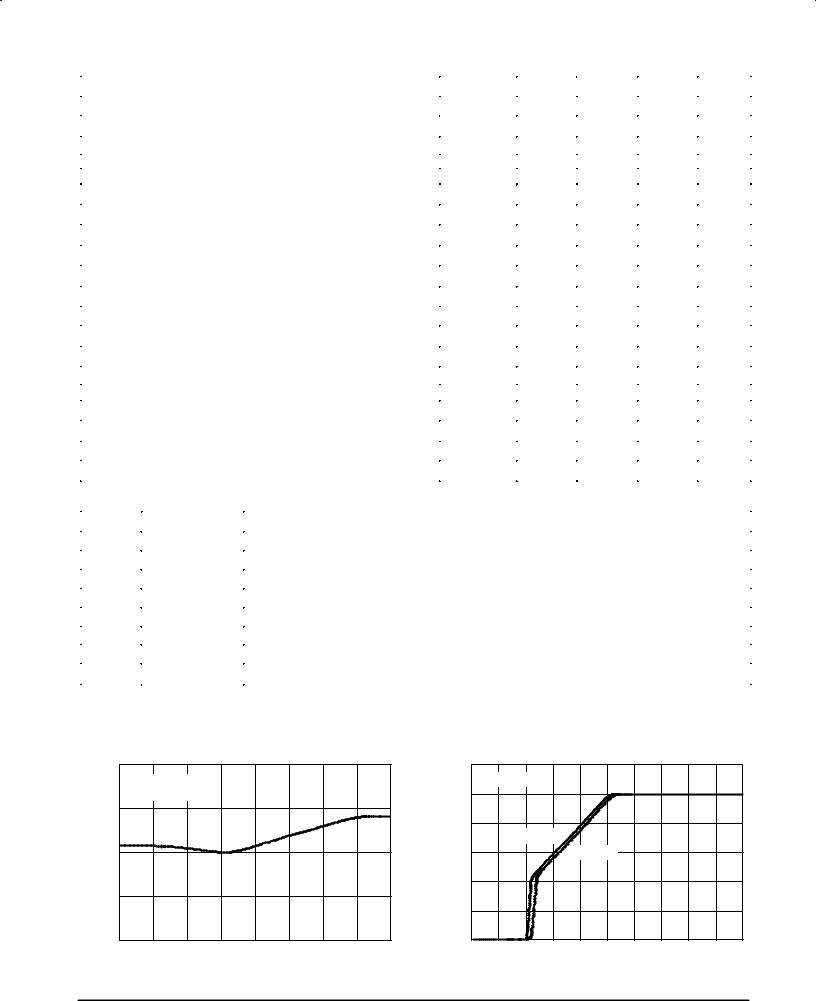
TYPICAL CHARACTERIZATION CURVES
Figure 1. Output Voltage versus |
Figure 2. Output Voltage versus |
Junction Temperature |
Supply Voltage |
|
5.04 |
|
|
|
|
|
|
|
|
6.0 |
|
|
VCC = 14 V |
|
|
|
|
|
|
5.0 |
|
(V) |
|
Iout = 1.0 mA |
|
|
|
|
|
(V) |
||
5.02 |
|
|
|
|
|
|
|
|
||
VOLTAGE |
|
|
|
|
|
|
|
VOLTAGE |
|
|
|
|
|
|
|
|
|
|
4.0 |
||
5.0 |
|
|
|
|
|
|
|
3.0 |
||
OUTPUT |
|
|
|
|
|
|
|
OUTPUT |
||
|
|
|
|
|
|
|
|
2.0 |
||
, |
4.98 |
|
|
|
|
|
|
|
, |
|
out |
|
|
|
|
|
|
|
out |
|
|
|
|
|
|
|
|
|
|
|
||
V |
|
|
|
|
|
|
|
|
V |
1.0 |
|
|
|
|
|
|
|
|
|
|
|
|
4.96 |
±20 |
0 |
20 |
40 |
60 |
80 |
100 |
120 |
0 |
|
±40 |
|
||||||||
|
|
|
TJ, JUNCTION TEMPERATURE (°C) |
|
|
|
||||
|
TJ = 25°C |
|
|
|
|
|
|
|
|
|
|
|
RL = 5.0 k |
|
|
|
|
|
|
|
|
|
|
|
|
RL = 100 Ω |
|
|
|
|
|
|
0 |
1.0 |
2.0 |
3.0 |
4.0 |
5.0 |
6.0 |
7.0 |
8.0 |
9.0 |
10 |
|
|
|
VCC, SUPPLY VOLTAGE (V) |
|
|
|
||||
MOTOROLA ANALOG IC DEVICE DATA |
3 |
|
 Loading...