


BZX84B12LT1G
ON BZX84B12LT1G, BZX84B15LT1G, BZX84B16LT1G, BZX84B18LT1G, BZX84B22LT1G Schematic [ru]
...
BZX84BxxxLT1G,
BZX84CxxxLT1G Series,
SZBZX84BxxxLT1G,
SZBZX84CxxxLT1G Series
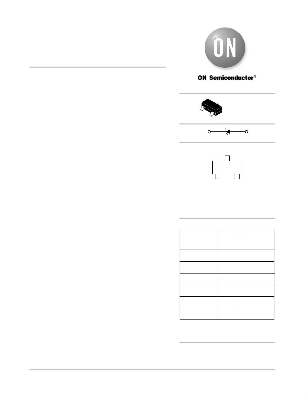
Zener Voltage Regulators
225 mW SOT−23 Surface Mount
http://onsemi.com
This series of Zener diodes is offered in the convenient, surface
mount plastic SOT−23 package. These devices are designed to provide
voltage regulation with minimum space requirement. They are well
suited for applications such as cellular phones, hand held portables,
and high density PC boards.
Features
• 225 mW Rating on FR−4 or FR−5 Board
• Zener Breakdown Voltage Range − 2.4 V to 75 V
• Package Designed for Optimal Automated Board Assembly
• Small Package Size for High Density Applications
• ESD Rating of Class 3 (> 16 kV) per Human Body Model
• Tight Tolerance Series Available (See Page 4)
• SZ Prefix for Automotive and Other Applications Requiring Unique
Site and Control Change Requirements; AEC−Q101 Qualified and
PPAP Capable
• These Devices are Pb−Free and are RoHS Compliant
Mechanical Characteristics
CASE:
Void-free, transfer-molded, thermosetting plastic case
FINISH: Corrosion resistant finish, easily Solderable
MAXIMUM CASE TEMPERATURE FOR SOLDERING PURPOSES:
260°C for 10 Seconds
POLARITY: Cathode indicated by polarity band
FLAMMABILITY RATING: UL 94 V−0
SOT−23
CASE 318
STYLE 8
3
Cathode
MARKING DIAGRAM
xxx M G
G
1
xxx = Device Code
M = Date Code*
G = Pb−Free Package
(Note: Microdot may be in either location)
*Date Code orientation may vary depending
upon manufacturing location.
ORDERING INFORMATION
Device Package Shipping
BZX84CxxxLT1G SOT−23
SZBZX84CxxxLT1G SOT−23
BZX84CxxxLT3G 10,000 /
SZBZX84CxxxLT3G 10,000 /
BZX84BxxxLT1G SOT−23
SZBZX84BxxxLT1G SOT−23
BZX84BxxxLT3G 10,000 /
†For information on tape and reel specifications,
including part orientation and tape sizes, please
refer to our Tape and Reel Packaging Specification
Brochure, BRD8011/D.
(Pb−Free)
(Pb−Free)
SOT−23
(Pb−Free)
SOT−23
(Pb−Free)
(Pb−Free)
(Pb−Free)
SOT−23
(Pb−Free)
1
Anode
3,000 /
Tape & Reel
3,000 /
Tape & Reel
Tape & Reel
Tape & Reel
3,000 /
Tape & Reel
3,000 /
Tape & Reel
Tape & Reel
†
*For additional information on our Pb−Free strategy and soldering details, please
download the ON Semiconductor Soldering and Mounting Techniques
Reference Manual, SOLDERRM/D.
© Semiconductor Components Industries, LLC, 2012
October, 2012 − Rev. 16
1 Publication Order Number:
DEVICE MARKING INFORMATION
See specific marking information in the device marking
column of the Electrical Characteristics table on page 3 of
this data sheet.
BZX84C2V4LT1/D
BZX84BxxxLT1G, BZX84CxxxLT1G Series, SZBZX84BxxxLT1G, SZBZX84CxxxLT1G
Series
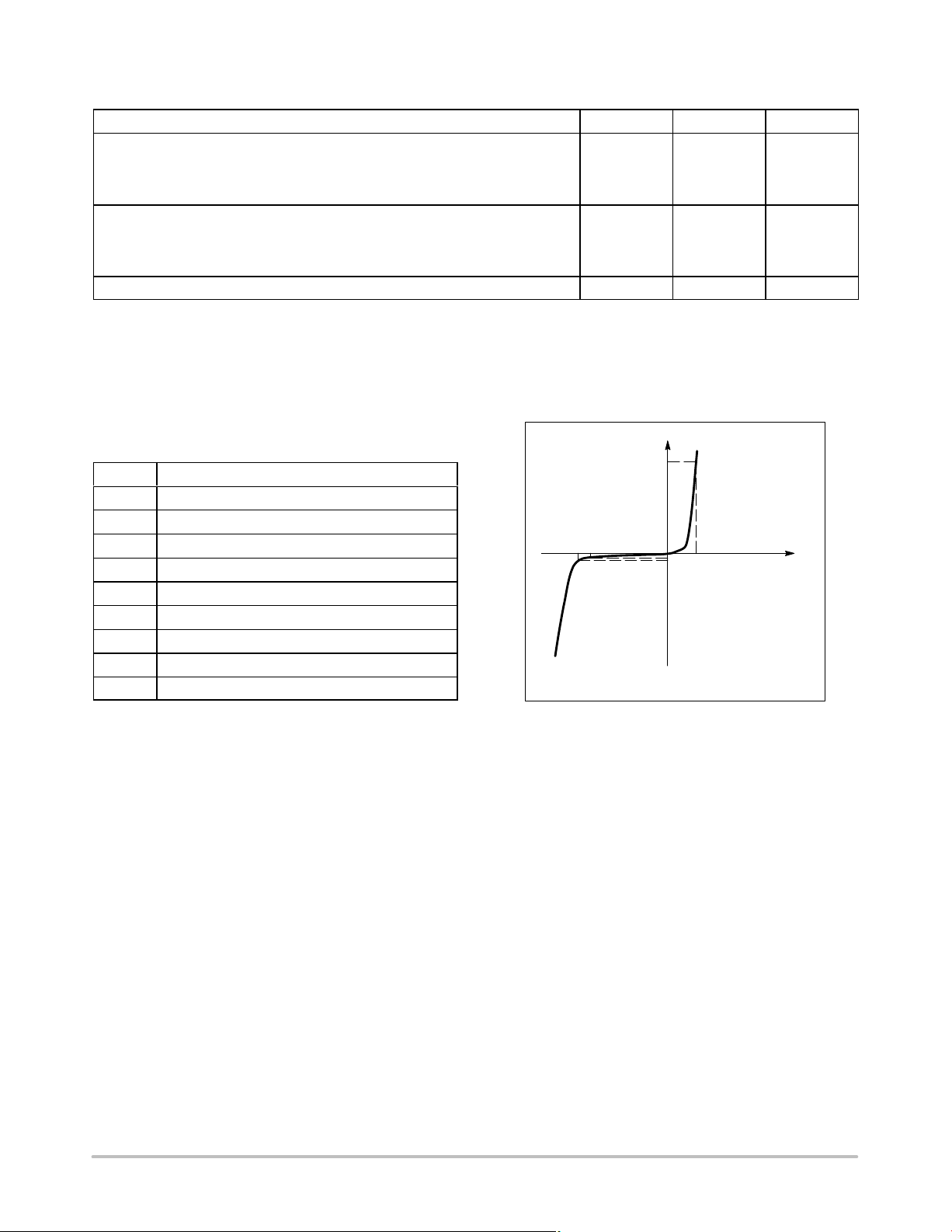
MAXIMUM RATINGS
Rating Symbol Max Unit
Total Power Dissipation on FR−5 Board,
(Note 1) @ T
Derated above 25°C
= 25°C
A
Thermal Resistance, Junction−to−Ambient
Total Power Dissipation on Alumina
Substrate, (Note 2) @ T
Derated above 25°C
= 25°C
A
Thermal Resistance, Junction−to−Ambient
Junction and Storage Temperature Range TJ, T
Stresses exceeding Maximum Ratings may damage the device. Maximum Ratings are stress ratings only. Functional operation above the
Recommended Operating Conditions is not implied. Extended exposure to stresses above the Recommended Operating Conditions may affect
device reliability.
1. FR−5 = 1.0 X 0.75 X 0.62 in.
2. Alumina = 0.4 X 0.3 X 0.024 in., 99.5% alumina.
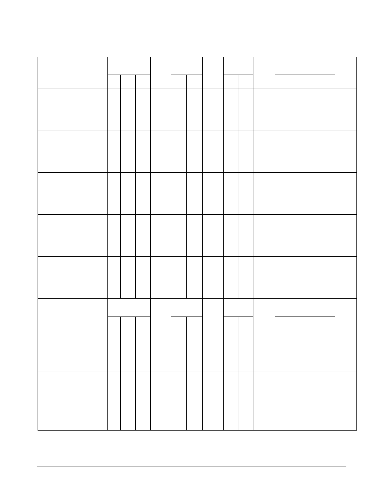
ELECTRICAL CHARACTERISTICS
(Pinout: 1-Anode, 2-No Connection, 3-Cathode) (TA = 25°C
unless otherwise noted, V
Symbol
V
I
Z
V
V
QV
Reverse Zener Voltage @ I
Z
Reverse Current
ZT
Maximum Zener Impedance @ I
ZT
I
Reverse Leakage Current @ V
R
Reverse Voltage
R
I
Forward Current
F
Forward Voltage @ I
F
Maximum Temperature Coefficient of V
Z
C Max. Capacitance @ VR = 0 and f = 1 MHz
= 0.90 V Max. @ IF = 10 mA)
F
Parameter
ZT
ZT
R
F
Z
P
D
R
q
JA
P
D
R
q
JA
stg
−65 to +150 °C
I
I
F
VRV
Z
I
V
R
I
ZT
Zener Voltage Regulator
F
225
1.8
556
300
2.4
417
mW
mW/°C
°C/W
mW
mW/°C
°C/W
V
http://onsemi.com
2
BZX84BxxxLT1G, BZX84CxxxLT1G Series, SZBZX84BxxxLT1G, SZBZX84CxxxLT1G
Series
ELECTRICAL CHARACTERISTICS − BZX84CxxxLT1 SERIES (STANDARD TOLERANCE)
(Pinout: 1-Anode, 2-No Connection, 3-Cathode) (TA = 25°C unless otherwise noted, VF = 0.90 V Max. @ IF = 10 mA)
(Devices listed in bold, italic are ON Semiconductor Preferred devices.)
VZ1 (Volts)
@I
=5mA
ZT1
(Note 3)
Device*
BZX84C2V4LT1G Z11 2.2 2.4 2.6 100 1.7 2.1 600 2.6 3.2 50 50 1 −3.5 0 450
BZX84C2V7LT1G Z12 2.5 2.7 2.9 100 1.9 2.4 600 3 3.6 50 20 1 −3.5 0 450
BZX84C3V0LT1G Z13 2.8 3 3.2 95 2.1 2.7 600 3.3 3.9 50 10 1 −3.5 0 450
BZX84C3V3LT1G Z14 3.1 3.3 3.5 95 2.3 2.9 600 3.6 4.2 40 5 1 −3.5 0 450
BZX84C3V6LT1G Z15 3.4 3.6 3.8 90 2.7 3.3 600 3.9 4.5 40 5 1 −3.5 0 450
BZX84C3V9LT1G Z16 3.7 3.9 4.1 90 2.9 3.5 600 4.1 4.7 30 3 1 −3.5 −2.5 450
BZX84C4V3LT1G W9 4 4.3 4.6 90 3.3 4 600 4.4 5.1 30 3 1 −3.5 0 450
BZX84C4V7LT1/T3G Z1 4.4 4.7 5 80 3.7 4.7 500 4.5 5.4 15 3 2 −3.5 0.2 260
BZX84C5V1LT1/T3G Z2 4.8 5.1 5.4 60 4.2 5.3 480 5 5.9 15 2 2 −2.7 1.2 225
BZX84C5V6LT1/T3G Z3 5.2 5.6 6 40 4.8 6 400 5.2 6.3 10 1 2 −2.0 2.5 200
BZX84C6V2LT1/T3G Z4 5.8 6.2 6.6 10 5.6 6.6 150 5.8 6.8 6 3 4 0.4 3.7 185
BZX84C6V8LT1/T3G Z5 6.4 6.8 7.2 15 6.3 7.2 80 6.4 7.4 6 2 4 1.2 4.5 155
BZX84C7V5LT1G Z6 7 7.5 7.9 15 6.9 7.9 80 7 8 6 1 5 2.5 5.3 140
BZX84C8V2LT1G Z7 7.7 8.2 8.7 15 7.6 8.7 80 7.7 8.8 6 0.7 5 3.2 6.2 135
BZX84C9V1LT1/T3G Z8 8.5 9.1 9.6 15 8.4 9.6 100 8.5 9.7 8 0.5 6 3.8 7.0 130
BZX84C10LT1G Z9 9.4 10 10.6 20 9.3 10.6 150 9.4 10.7 10 0.2 7 4.5 8.0 130
BZX84C11LT1G Y1 10.4 11 11.6 20 10.2 11.6 150 10.4 11.8 10 0.1 8 5.4 9.0 130
BZX84C12LT1G Y2 11.4 12 12.7 25 11.2 12.7 150 11.4 12.9 10 0.1 8 6.0 10.0 130
BZX84C13LT1G Y3 12.4 13 14.1 30 12.3 14 170 12.5 14.2 15 0.1 8 7.0 11.0 120
BZX84C15LT1/T3G Y4 13.8 15 15.6 30 13.7 15.5 200 13.9 15.7 20 0.05 10.5 9.2 13.0 11 0
BZX84C16LT1G Y5 15.3 16 17.1 40 15.2 17 200 15.4 17.2 20 0.05 11.2 10.4 14.0 105
BZX84C18LT1/T3G Y6 16.8 18 19.1 45 16.7 19 225 16.9 19.2 20 0.05 12.6 12.4 16.0 100
BZX84C20LT1G Y7 18.8 20 21.2 55 18.7 21.1 225 18.9 21.4 20 0.05 14 14.4 18.0 85
BZX84C22LT1G Y8 20.8 22 23.3 55 20.7 23.2 250 20.9 23.4 25 0.05 15.4 16.4 20.0 85
BZX84C24LT1G Y9 22.8 24 25.6 70 22.7 25.5 250 22.9 25.7 25 0.05 16.8 18.4 22.0 80
Device*
BZX84C27LT1G Y10 25.1 27 28.9 80 25 28.9 300 25.2 29.3 45 0.05 18.9 21.4 25.3 70
BZX84C30LT1G Y11 28 30 32 80 27.8 32 300 28.1 32.4 50 0.05 21 24.4 29.4 70
BZX84C33LT1/T3G Y12 31 33 35 80 30.8 35 325 31.1 35.4 55 0.05 23.1 27.4 33.4 70
BZX84C36LT1G Y13 34 36 38 90 33.8 38 350 34.1 38.4 60 0.05 25.2 30.4 37.4 70
BZX84C39LT1G Y14 37 39 41 130 36.7 41 350 37.1 41.5 70 0.05 27.3 33.4 41.2 45
BZX84C43LT1G Y15 40 43 46 150 39.7 46 375 40.1 46.5 80 0.05 30.1 37.6 46.6 40
BZX84C47LT1G Y16 44 47 50 170 43.7 50 375 44.1 50.5 90 0.05 32.9 42.0 51.8 40
BZX84C51LT1G Y17 48 51 54 180 47.6 54 400 48.1 54.6 100 0.05 35.7 46.6 57.2 40
BZX84C56LT1G Y18 52 56 60 200 51.5 60 425 52.1 60.8 110 0.05 39.2 52.2 63.8 40
BZX84C62LT1G Y19 58 62 66 215 57.4 66 450 58.2 67 120 0.05 43.4 58.8 71.6 35
BZX84C68LT1G Y20 64 68 72 240 63.4 72 475 64.2 73.2 130 0.05 47.6 65.6 79.8 35
BZX84C75LT1G Y21 70 75 79 255 69.4 79 500 70.3 80.2 140 0.05 52.5 73.4 88.6 35
Device
Marking
Device
Marking
Min Nom Max Min Max Min Max
VZ1 Below
@I
=2mA
ZT1
Min Nom Max Min Max Min Max
Z
@ I
5 mA
Z
Below
@ I
2 mA
(W)
ZT1
ZT1
ZT1
ZT1
3. Zener voltage is measured with a pulse test current IZ at an ambient temperature of 25°C.
*Include SZ-prefix devices where applicable.
=
=
VZ2 (V)
@I
ZT2
(Note 3)
VZ2 Below
@I
ZT2
=1mA
= 0.1 m-
A
Z
ZT2
(W)
@ I
ZT2
1 mA
Z
ZT2
Below
@ I
ZT4
0.5 mA
=
=
VZ3 (V)
@I
ZT3
(Note 3)
VZ3 Below
@I
ZT3
=20mA
=10mA
Z
@ I
20 mA
Z
Below
@ I
10 mA
(W)
ZT3
ZT3
ZT3
ZT3
=
=
Max Reverse
Leakage
Current
V
I
R
@
Volts
mA
Max Reverse
Leakage
Current
V
I
R
@
(V)
mA
R
R
q
VZ
(mV/k)
= 5 mA
@ I
ZT1
Min Max
q
VZ
(mV/k) Below
@ I
= 2 mA
ZT1
Min Max
@ V
f = 1 MHz
@ V
f = 1 MHz
C (pF)
R
C (pF)
R
= 0
= 0
http://onsemi.com
3
 Loading...