


OMNIREL OM6N100SA, OM3N100ST, OM1N100ST, OM5N100SA, OM3N100SA Datasheet
...
OM1N100SA OM5N100SA OM1N100ST
OM3N100SA OM6N100SA OM3N100ST
POWER MOSFET IN HERMETIC ISOLATED JEDEC PACKAGE
1000V, Up To 6 Amp, N-Channel
MOSFET In Hermetic Metal Package
FEATURES
•Isolated Hermetic Metal Package
•Fast Switching
•Low RDS(on)
•Available Screened To MIL-19500, TX, TXV And S
•Ceramic Feedthroughs Also Available
DESCRIPTION
This series of hermetically packaged products feature the latest advanced MOSFET and packaging technology. They are ideally suited for Military requirements where small size, high performance and high reliability are required, and in applications such as switching power supplies, motor controls, inverters, choppers, audio amplifiers and high energy pulse circuits.
MAXIMUM RATINGS
PART NUMBER |
RDS(on) |
|
ID |
|
|
|||||
OM1N100SA |
8.0 |
|
1.0A |
|
|
|||||
OM3N100SA |
5.2 |
|
3.5A |
|
|
|||||
3.1 |
||||||||||
OM5N100SA |
3.0 |
|
5.0A |
|
||||||
OM6N100SA |
2.0 |
|
6.0A |
|
|
|||||
OM3N100ST |
5.4 |
|
3.5A |
|
|
|||||
OM1N100ST |
8.2 |
|
1.0A |
|
|
|||||
|
|
|
|
|
|
|
|
|
||
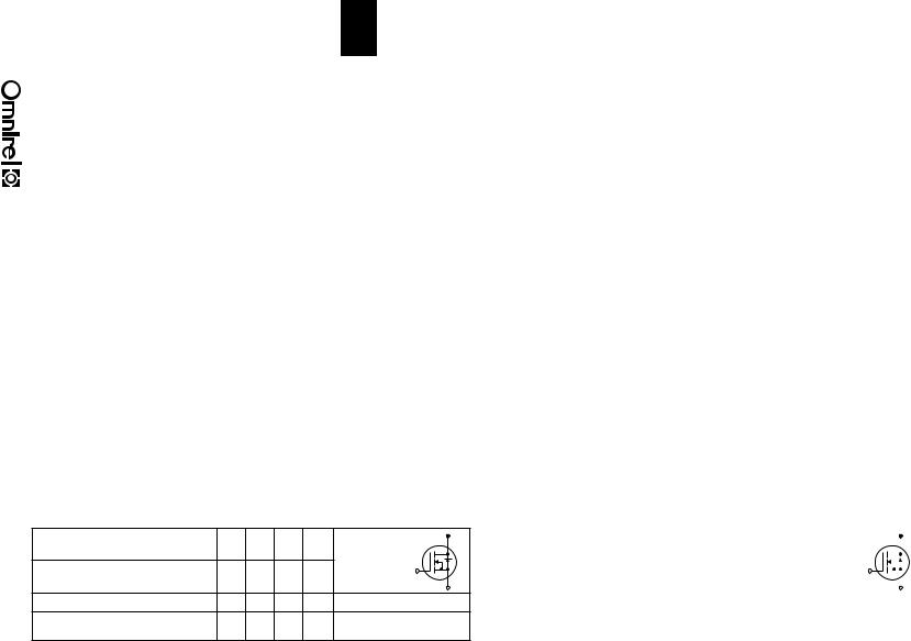
SCHEMATIC |
|
PIN CONNECTION |
|
|||||||
|
|
DRAIN |
TO-254AA |
|
|
TO-257AA |
|
|||
|
|
|
|
|
||||||
|
|
|
|
|
|
|
|
|
|
|
|
|
|
|
|
|
|
|
|
|
|
GATE
|
|
|
Pin 1: Drain |
|
|
|
|
|
|
Pin 2: Source |
|
|
|
1 |
2 |
3 |
Pin 3: Gate |
1 |
2 |
3 |
SOURCE |
|
|
|
|
|
|
4 11 R1 |
3.1 - 15 |
Supersedes 2 05 R0 |
16 - 1.3
1.3
ELECTRICAL CHARACTERISTICS: TC = 25° unless otherwise noted
STATIC P/N OM1N100SA (See Note 3)
Parameter |
Min. |
Typ. |
Max. |
Units |
Test Conditions |
|
|
|
|
|
|
|
|
BVDSS |
Drain-Source Breakdown |
1000 |
|
|
V |
VGS = 0, |
|
Voltage |
|
|
|
|
ID = 250 mA |
|
|
|
|
|
|
|
VGS(th) |
Gate-Threshold Voltage |
2.0 |
|
4.0 |
V |
VDS = VGS, ID = 250 mA |
IGSSF |
Gate-Body Leakage Forward |
|
|
100 |
nA |
VGS = 20 V, VDS = 0 |
IGSSR |
Gate-Body Leakage Reverse |
|
|
-100 |
nA |
VGS = - 20 V, VDS = 0 |
IDSS |
Zero Gate Voltage |
|
|
0.25 |
mA |
VDS = Max. Rat., VGS = 0 |
|
Drain Current |
|
|
1.0 |
mA |
VDS = 0.8 x Max. Rat., |
|
|
|
|
|
|
VGS = 0, TC = 125° C |
|
|
|
|
|
|
|
ID(on) |
On-State Drain Current |
1.0 |
|
|
A |
VDS > ID(on) x RDS(on) Max. |
|
|
|
|
|
|
VGS = 10 V |
RDS(on) |
Static Drain-Source On-State |
|
SA |
8.0 |
|
VGS = 10 V |
|
Resisitance1, 3 |
|
ST |
8.2 |
|
ID =.5A |
RDS(on) |
Static Drain-Source On-State |
|
SA |
15.0 |
|
VGS = 10 V |
|
Resistance1, 3 |
|
ST |
15.4 |
|
ID =.5A, TC = 100° C |
DYNAMIC
gfs |
Forward Transductance |
1.0 |
|
|
S |
VDS = 10V, ID = 1 A |
Ciss |
Input Capacitance |
|
950 |
|
pF |
VGS = 0 |
Coss |
Output Capacitance |
|
110 |
|
pF |
VDS = 25 V |
Crss |
Reverse Transfer Capacitance |
|
40 |
|
pF |
f = 1 MHz |
Td(on) |
Turn-On Delay Time |
|
90 |
|
ns |
|
tr |
Rise Time |
|
90 |
|
ns |
|
Td(off) |
Turn-Off Delay Time |
|
115 |
|
ns |
VDD = 600 V, ID = 3.5 |
tf |
Fall Time |
|
75 |
|
ns |
RG = 50W, VGS = 10 V |
ELECTRICAL CHARACTERISTICS: TC = 25° unless otherwise noted
STATIC P/N OM3N100SA (See Note 3)
Parameter |
Min. |
Typ. |
Max. |
Units |
Test Conditions |
|
|
|
|
|
|
|
|
BVDSS |
Drain-Source Breakdown |
1000 |
|
|
V |
VGS = 0, |
|
Voltage |
|
|
|
|
ID = 250 mA |
|
|
|
|
|
|
|
VGS(th) |
Gate-Threshold Voltage |
2.0 |
|
4.0 |
V |
VDS = VGS, ID = 250 mA |
IGSSF |
Gate-Body Leakage Forward |
|
|
100 |
nA |
VGS = 20 V |
IGSSR |
Gate-Body Leakage Reverse |
|
|
- 100 |
nA |
VGS = - 20 V |
IDSS |
Zero Gate Voltage Drain |
|
|
0.25 |
mA |
VDS = Max. Rat., VGS = 0 |
|
Current |
|
|
1.0 |
mA |
VDS = 0.8 x Max. Rat., |
|
|
|
|
|
|
VGS = 0, TC = 125° C |
|
|
|
|
|
|
|
ID(on) |
On-State Drain Current |
3.5 |
|
|
A |
VDS > ID(on) x RDS(on) Max |
|
|
|
|
|
|
VGS = 10 V |
RDS(on) |
Static Drain-Source On-State |
|
SA |
5.2 |
|
VGS = 10 V |
|
Resistance1, 3 |
|
ST |
5.4 |
|
ID =.5A |
RDS(on) |
Static Drain-Source On-State |
|
SA |
10.0 |
|
VGS = 10 V |
|
Resistance 1, 3 |
|
ST |
10.4 |
|
ID =.5A, TC = 100° C |
DYNAMIC
gfs |
Forward Transductance |
1.0 |
|
|
S |
VDS = 10, ID = 1.5 A |
Ciss |
Input Capacitance |
|
950 |
|
pF |
VGS = 0 |
Coss |
Output Capacitance |
|
110 |
|
pF |
VDS = 25 V |
Crss |
Reverse Transfer Capacitance |
|
40 |
|
pF |
f = 1 MHz |
Td(on) |
Turn-On Delay Time |
|
90 |
|
ns |
|
tr |
Rise Time |
|
90 |
|
ns |
|
Td(off) |
Turn-Off Delay Time |
|
115 |
|
ns |
VDD = 600 V, ID = 3.5 |
tf |
Fall Time |
|
75 |
|
ns |
RG = 50W, VGS = 10 V |
BODY-DRAIN DIODE RATINGS AND CHARACTERISTICS
IS |
Continuous Source Current |
3.5 |
A |
Modified MOSPOWER |
D |
|
|
||||||
|
(Body Diode) |
|
|
symbol showing |
|
|
ISM |
Source Current1 |
14 |
A |
the integral P-N |
G |
|
|
|
|||||
|
(Body Diode) |
|
|
Junction rectifier. |
|
S |
VSD |
Diode Forward Voltage2 |
2.5 |
V |
TC = 25 C, IS = 3.5 A, VGS = 0 |
||
trr |
Reverse Recovery Time |
900 |
ns |
IF = IS, VDD = 100 V |
|
|
|
|
|
|
dlF/ds = 100 A/ms, TJ = 150 C |
||
1 Pulse Test: Pulse Width 300msec, Duty Cycle 1.5%. 2 Pulse Width limited by safe operating area.
3 OM1N100ST - All characteristics the same except RDS(on)
BODY-DRAIN DIODE RATINGS AND CHARACTERISTICS
IS |
Continuous Source Current |
|
|
3.5 |
A |
Modified MOSPOWER |
|
|
|
|
D |
|||
|
(Body Diode) |
|
|
|
|
symbol showing |
|
|
|
|
|
|
|
|
|
|
|
|
|
G |
|
|
|
|
|
|
|||
ISM |
Source Current1 |
|
|
14 |
A |
the integral P-N |
|
|
|
|
|
|
||
|
|
|
|
|
|
|
|
|
|
|||||
|
(Body Diode) |
|
|
|
|
Junction rectifier. |
|
|
|
|
|
|
S |
|
|
|
|
|
|
|
|
|
|
|
|
||||
VSD |
Diode Forward Voltage2 |
|
|
2.5 |
V |
TC = 25 C, IS = 3.5 A, VGS = 0 |
||||||||
trr |
Reverse Recovery Time |
|
900 |
|
ns |
IF = IS, VDD = 100 V |
|
|
|
|
|
|
||
|
|
|
|
|
|
dlF/ds = 100 A/ms, TJ = 150 C |
||||||||
1 Pulse Test: Pulse Width 300msec, Duty Cycle 1.5%. |
|
|
|
|
|
|
|
|
|
|
||||
2 Pulse Width limited by safe operating area. |
|
|
|
|
|
|
|
|
|
|
|
|
||
3 OM3N100ST - All characteristics the same except RDS(on)
Series OM1N100SA/ST
 Loading...