


LPC2101
Table of contents
 Loading...
UM10161
LPC2101/02/03 User manual
Rev. 4 — 13 May 2009 User manual
Document information
Info Content
Keywords LPC2101, LPC2102, LPC2103, ARM, ARM7, embedded, 32-bit,
microcontroller
Abstract LPC2101/02/03 User manual revision

NXP Semiconductors
UM10161
LPC2101/02/03 User manual
Revision history
Rev Date Description
04 20090513 LPC2101/02/03 User manual
Modifications:
• Description of Deep power-down mode and power selector module added (LPC2101/02/03 revisions A and higher
only). See Section 5–10
, Section 18–6.14, and Section 18–7.
• Description of three CRP levels added (LPC2101/02/03 revisions A and higher only). See Section 19–8.
03 20081002 LPC2101/02/03 User manual
Modifications:
• Description of pins VBAT, RTCX1, RTCX2, V
DDA
, and V
DD(1V8)
updated.
• Bit description for bits CPOL and CPHA in SSPCR0 register updated.
• Pin description for ADC pins updated.
• PLCC44 pin configuration removed.
• HVQFN48 pin configuration added.
2
• I
C pin description in pin configuration updated.
• Timer2/3 register names PWM2/3CON updated.
• Description of JTAG pin TCK updated.
• Bit description in CTC register updated.
• Various editorial updates.
• Description of fractional baudrate generator updated for UART0 and UART1.
• Bit description of the PCONP register updated.
02 20070801 LPC2101/02/03 User manual
Modifications:
• SCL1 and SDA1 pins described as not open-drain.
01 20060112 Initial version
Contact information
For more information, please visit: http://www.nxp.com
For sales office addresses, please send an email to: salesaddresses@nxp.com
UM10161_4 © NXP B.V. 2009. All rights reserved.
User manual Rev. 4 — 13 May 2009 2 of 292

1. Introduction
UM10161
Chapter 1: LPC2101/02/03 Introductory information
Rev. 4 — 13 May 2009 User manual
The LPC2101/02/03 microcontrollers are based on a 16-bit/32-bit ARM7TDMI-S CPU with
real-time emulation that combines the microcontroller with 8 kB, 16 kB, or 32 kB of
embedded high speed flash memory. A 128-bit wide memory interface and a unique
accelerator architecture enable 32-bit code execution at the maximum clock rate. For
critical performance in interrupt service routines and DSP algorithms, this increases
performance up to 30 % over the Thumb mode. For critical code size applications, the
alternative 16-bit Thumb mode reduces code by more than 30 % with minimal
performance penalty.
Due to their tiny size and low power consumption, LPC2101/02/03 are ideal for
applications where miniaturization is a key requirement, such as access control and
point-of-sale. A blend of serial communications interfaces, ranging from multiple UARTS,
SPI, and SSP to two I
suited for communication gateways and protocol converters. The superior performance
also makes these devices suitable as math coprocessors. Various 32-bit and 16-bit
timers, an improved 10-bit ADC, PWM features through output match on all timers, and 32
fast GPIO lines with up to 13 edge or level sensitive external interrupt pins make these
microcontrollers particularly suitable for industrial control and medical systems.
2
Cs, and on-chip SRAM of 2/4/8 kB make these devices very well
2. How to read this manual
This user manual describes parts LPC2101/02/03 Revision ‘-’ and parts LPC2101/02/03
Revision A and higher. Differences between Revision ‘-’ and others are described at the
beginning of each chapter if applicable and are summarized as follows:
Revision ‘-’: One CRP level; Power-down modes: idle and power-down.
Revision A and higher: Three CRP levels; Power-down modes: idle, power-down, and
deep power-down.
3. Enhanced features
Starting with Revision A, the LPC2101/02/03 have the following enhanced features
implemented:
• Deep power-down mode controlled by the RTC block.
• Three levels of Code Read Protection (CRP).
4. Features
• 16-bit/32-bit ARM7TDMI-S microcontroller in a tiny LQFP48 p ackage.
• 2 kB/4 kB/8 kB of on-chip static RAM and 8 kB/16 kB/32 kB of on-chip flash program
memory. 128-bit wide interface/accelerator enables high-speed 70 MHz operation.
UM10161_4 © NXP B.V. 2009. All rights reserved.
User manual Rev. 4 — 13 May 2009 3 of 292

NXP Semiconductors
• In-System/In-Application Programming (ISP/IAP) via on-chip boot loader software.
• EmbeddedICE RT offers real-time de bugging with the on-chip RealMonitor software.
• The 10-bit A/D converter provides eight analog inputs, with conversion times as low
• Two 32-bit timers/external event counters with combined seven capture and seve n
• Two 16-bit timers/external event counters with combined three capture and seven
• Low power Real-Time Clock (RTC) with independent power and dedicated 32 kHz
• Multiple serial interfaces including two UARTs (16C550), two Fast I
• Vectored interrupt controller with configurable priorities and vector addresses.
• Up to thirty-two 5 V tolerant fast general purpose I/O pins.
• Up to 13 edge or level sensitive external interrupt pins available.
• 70 MHz maximum CPU clock available from programmable on-chip PLL with a
• On-chip integrated oscillator operates with an external crystal in the range from
• Power saving modes include Idle mode, Power-down mode, and Power-down mode
• Individual enable/disable of peripheral functions as well as peripheral clock scaling for
• Processor wake-up from Power-down mode via external interrupt or RTC.
UM10161
Chapter 1: LPC2101/02/03 Introductory information
Single flash sector or full chip erase in 100 ms and programming of 2 56 bytes in 1 ms.
as 2.44 μs per channel, and dedicated result registers to minimize interrupt overhead.
compare channels.
compare channels.
clock input.
2
C-buses
(400 kbit/s), SPI and SSP with buffering and variable data length capabilities.
possible input frequency of 10 MHz to 25 MHz and a settling time of 100 μs.
1 MHz to 25 MHz.
with RTC active.
additional power optimization.
5. Applications
• Industrial control
• Medical systems
• Access control
• Point-of-sale
• Communication gateway
• Embedded soft modem
• General purpose applications
UM10161_4 © NXP B.V. 2009. All rights reserved.
User manual Rev. 4 — 13 May 2009 4 of 292

NXP Semiconductors
6. Device information
Table 1. LPC2101/02/03 device information
Type number Flash memory RAM ADC Temperature
LPC2101FBD48 8 kB 2 kB 8 inputs −40 to +85
LPC2102FBD48 16 kB 4 kB 8 inputs −40 to +85
LPC2103FBD48 32 kB 8 kB 8 inputs −40 to +85
LPC2102FHN48 16 kB 4 kB 8 inputs −40 to +85
LPC2103FHN48 32 kB 8 kB 8 inputs −40 to +85
LPC2103FHN48H 32 kB 8 kB 8 inputs −40 to +85
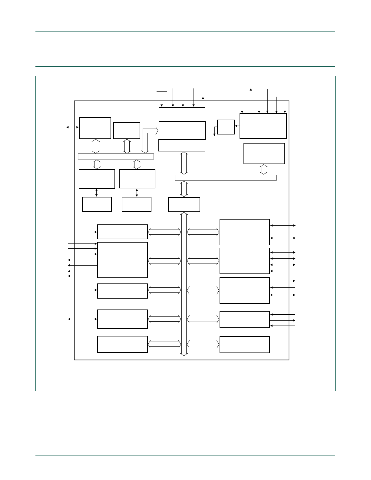
7. Architectural overview
The LPC2101/02/03 consist of an ARM7TDMI-S CPU with emulation support, the ARM7
Local Bus for interface to on-chip memory controllers, the AMBA Advanced
High-performance Bus (AHB) for interface to the interrupt controller, and the ARM
Peripheral Bus (APB, a compatible superset of ARM’s AMBA Advanced Peripheral Bus)
for connection to on-chip peripheral functions. The LPC2101/02/03 configures the
ARM7TDMI-S processor in little-endian byte order.
UM10161
Chapter 1: LPC2101/02/03 Introductory information
range (°C)
AHB peripherals are allocated a 2 megabyte range of addresses at the very top of the
4 gigabyte ARM memory space. Each AHB peripheral is allocated a 16 kB address space
within the AHB address space. LPC2101/02/03 peripheral functions (other than the
interrupt controller) are connected to the APB bus. The AHB to APB bridge interfaces the
APB bus to the AHB bus. APB peripherals are also allocated a 2 megabyte range of
addresses, beginning at the 3.5 gigabyte address point. Each APB peripheral is allocated
a 16 kB address space within the APB address space.
The connection of on-chip peripherals to device pins is controlled by a Pin Connect Block
(see Section 7–4 on page 70
application requirements for the use of peripheral functions and pins.
8. ARM7TDMI-S processor
The ARM7TDMI-S is a general purpose 32-bit microprocessor, which offers high
performance and very low power consumption. The ARM architecture is based on
Reduced Instruction Set Computer (RISC) principles, and the instruction set and related
decode mechanism are much simpler than those of microprogrammed Complex
Instruction Set Computers. This simplicity results in a high instruction throughput and
impressive real-time interrupt response from a small and cost-effective processor core.
Pipeline techniques are employed so that all pa rts of the p rocessing and memory systems
can operate continuously. T ypically, while one instruction is being executed, its successor
is being decoded, and a third instruction is being fetched from memory.
). This must be configured by software to fit specific
The ARM7TDMI-S processor also employs a unique architectural strategy known as
THUMB, which makes it ideally suited to high-volume applications with memory
restrictions, or applications where code density is an issue.
UM10161_4 © NXP B.V. 2009. All rights reserved.
User manual Rev. 4 — 13 May 2009 5 of 292

NXP Semiconductors
The key idea behind THUMB is that of a super-reduced instruction set. Essentially, the
ARM7TDMI-S processor has two instruction sets:
• The standard 32-bit ARM instruction set.
• A 16-bit THUMB instruction set.
The THUMB set’s 16-bit instruction length allows it to approach twice the density of
standard ARM code while retaining most of the ARM’s performance advantage over a
traditional 16-bit processor using 16-bit registers. This is possible because THUMB code
operates on the same 32-bit register set as ARM code.
THUMB code is able to provide up to 65% of the code size of ARM, and 160% of the
performance of an equivalent ARM processor connected to a 16-bit memory system.
The ARM7TDMI-S processor is described in detail in the ARM7TDMI-S data sheet that
can be found on official ARM website.
9. On-chip flash memory system
UM10161
Chapter 1: LPC2101/02/03 Introductory information
The LPC2101/02/03 incorporate a 8 kB, 16 kB, and 32 kB flash memory system
respectively. This memory may be used for both code and data storage. Programming of
the flash memory may be accomplished in several ways:
• using the serial built-in JTAG interface
• using In System Programming (ISP) and UART
• using In Application Programming (IAP) capabilities
The application program, using the IAP functions, may also erase and/or program the
flash while the application is running, allowing a great degree of flexibility for dat a storage
field firmware upgrades, etc. The entire flash memory is available for user code because
the boot loader resides in a separate memory location.
The LPC2101/02/03 flash memory provides minimum of 100,000 erase/write cycles and
20 years of data-retention.
10. On-chip Static RAM (SRAM)
On-chip Static RAM (SRAM) may be used for code and/or data storage. The on-chip
SRAM may be accessed as 8-bits, 16-bits, and 32-bits. The LPC2101/02/03 provide
2/4/8 kB of static RAM respectively.
The LPC2101/02/03 SRAM is designed to be accessed as a byte-addressed memory.
Word and halfword accesses to the memory ignore the alignment of the address and
access the naturally-aligned value that is addressed (so a memory access ignores
address bits 0 and 1 for word accesses, and ignores bit 0 for halfword accesses).
Therefore valid reads and writes require data accessed as halfwords to originate from
addresses with address line 0 being 0 (addresses ending with 0, 2, 4, 6, 8, A, C, and E in
hexadecimal notation) and data accessed as words to originate from addresses with
address lines 0 and 1 being 0 (addresses ending with 0, 4, 8, and C in hexadecimal
notation).
UM10161_4 © NXP B.V. 2009. All rights reserved.
User manual Rev. 4 — 13 May 2009 6 of 292

NXP Semiconductors
The SRAM controller incorporates a write-back buffer in order to prevent CPU stalls
during back-to-back writes. The write-back buffer always holds the last data sent by
software to the SRAM. This data is only written to the SRAM when another write is
requested by software (the data is only written to the SRAM when software does another
write). If a chip reset occurs, actual SRAM contents will not reflect the most recent write
request (i.e. after a "warm" chip reset, the SRAM does not reflect the last wr ite operation).
Any software that checks SRAM contents after reset must take this into account. Two
identical writes to a location guarantee that the data will be present after a Reset.
Alternatively, a dummy write operation before entering idle or power-down mode will
similarly guarantee that the last data written will be present in SRAM after a subsequent
Reset.
UM10161
Chapter 1: LPC2101/02/03 Introductory information
UM10161_4 © NXP B.V. 2009. All rights reserved.
User manual Rev. 4 — 13 May 2009 7 of 292
NXP Semiconductors
002aab814
system
clock
TRST
TMS
TCK
TDI
TDO
XTAL2 V
DD(3V3)
XTAL1
AMBA AHB
(Advanced High-performance Bus)
MEMORY
ACCELERATOR
AHB BRIDGE
TEST/DEBUG
INTERFACE
AHB TO APB
BRIDGE
VECTORED
INTERRUPT
CONTROLLER
SYSTEM
FUNCTIONS
PLL
8 kB/16 kB/
32 kB FLASH
ARM7TDMI-S
LPC2101/2102/2103
INTERNAL
SRAM
CONTROLLER
2 kB/4 kB/
8 kB SRAM
ARM7 local bus
APB (ARM
peripheral bus)
SCL0, SCL1
(1)
SDA0, SDA1
(1)
3 × CAP0
(1)
4 × CAP1
(1)
3 × CAP2
(1)
3 × MAT0
(1)
4 × MAT1
(1)
3 × MAT2
(1)
4 × MAT3
(1)
AD0[7:0]
I
2
C-BUS SERIAL
INTERFACES 0 AND 1
CAPTURE/COMPARE
EXTERNAL COUNTER
TIMER 0/TIMER 1/
TIMER 2/TIMER 3
EINT2 to
EINT0
(1)
EXTERNAL
INTERRUPTS
SCK0, SCK1
(1)
MOSI0, MOSI1
(1)
MISO0, MISO1
(1)
SSEL0, SSEL1
(1)
SPI AND SSP
SERIAL INTERFACES
ADC
TXD0, TXD1
(1)
RXD0, RXD1
(1)
UART0/UART1
RTCX2
RTCX1
VBAT
REAL-TIME CLOCK
WATCHDOG
TIMER
SYSTEM CONTROL
P0[31:0]
P0[31:0]
GENERAL
PURPOSE I/O
HIGH SPEED
GENERAL
PURPOSE I/O
RST V
SS
8 kB
BOOT ROM
V
DD(1V8)
DSR1, CTS1,
RTS1, DTR1
DCD1, RI1
11. Block diagram
UM10161
Chapter 1: LPC2101/02/03 Introductory information
(1) Pins shared with GPIO.
Fig 1. LPC2101/02/03 block diagram
UM10161_4 © NXP B.V. 2009. All rights reserved.
User manual Rev. 4 — 13 May 2009 8 of 292

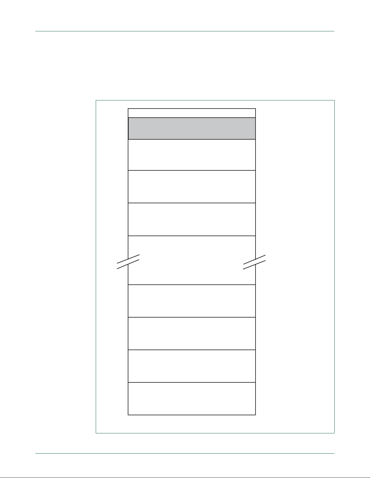
0.0 GB
1.0 GB
8 kB ON-CHIP NON-VOLATILE MEMORY
0x0000 2000
0x0000 1FFF
0x0000 0000
RESERVED ADDRESS SPACE
2 kB ON-CHIP STATIC RAM (LPC2101)
4 kB ON-CHIP STATIC RAM (LPC2102)
8 kB ON-CHIP STATIC RAM (LPC2103)
RESERVED ADDRESS SPACE
0x4000 0800
0x4000 07FF
0x4000 1000
0x4000 0FFF
0x4000 2000
0x4000 1FFF
0x4000 0000
2.0 GB
0x8000 0000
BOOT BLOCK
0x7FFF DFFF
0x7FFF E000
3.0 GB 0xC000 0000
RESERVED ADDRESS SPACE
3.75 GB
4.0 GB
3.5 GB
AHB PERIPHERALS
APB PERIPHERALS
0xE000 0000
0xF000 0000
0xFFFF FFFF
16 kB ON-CHIP NON-VOLATILE MEMORY
32 kB ON-CHIP NON-VOLATILE MEMORY
0x0000 4000
0x0000 3FFF
0x0000 8000
0x0000 7FFF
1. Memory maps
The LPC2101/02/03 incorporates several distin ct memory r egions, sh own in the fol lowing
figures. Figure 2–2
program viewpoint following reset. The interrupt vector area supports address remapping,
which is described later in this section.
UM10161
Chapter 2: LPC2101/02/03 Memory addressing
Rev. 4 — 13 May 2009 User manual
shows the overall map of the entire address space from the user
UM10161_4 © NXP B.V. 2009. All rights reserved.
User manual Rev. 4 — 13 May 2009 9 of 292
Fig 2. System memory map

NXP Semiconductors
RESERVED
RESERVED
0xF000 0000
0xEFFF FFFF
APB PERIPHERALS
0xE020 0000
0xE01F FFFF
0xE000 0000
AHB PERIPHERALS
0xFFFF FFFF
0xFFE0 0000
0xFFDF FFFF
3.75 GB
3.5 GB
3.5 GB + 2 MB
4.0 GB - 2 MB
4.0 GB
UM10161
Chapter 2: LPC2101/02/03 Memory addressing
AHB section is 128 x 16 kB blocks (totaling 2 MB).
APB section is 128 x 16 kB blocks (totaling 2MB).
Fig 3. Peripheral memory map
Figure 2–3, Figure 2–4, and Table 2–2 show different views of the peripheral address
space. Both the AHB and APB peripheral areas ar e 2 megabyte sp aces which are divided
up into 128 peripherals. Each peripheral space is 16 kilobytes in size. This allows
simplifying the address decoding for each peripheral. All peripheral regi ster addresses are
UM10161_4 © NXP B.V. 2009. All rights reserved.
User manual Rev. 4 — 13 May 2009 10 of 292
NXP Semiconductors
VECTORED INTERRUPT CONTROLLER
(AHB PERIPHERAL #0)
0xFFFF F000 (4G - 4K)
0xFFFF C000
0xFFFF 8000
(AHB PERIPHERAL #125)
(AHB PERIPHERAL #124)
(AHB PERIPHERAL #3)
(AHB PERIPHERAL #2)
(AHB PERIPHERAL #1)
(AHB PERIPHERAL #126)
0xFFFF 4000
0xFFFF 0000
0xFFE1 0000
0xFFE0 C000
0xFFE0 8000
0xFFE0 4000
0xFFE0 0000
word aligned (to 32-bit boundaries) regardless of their size. This eliminates the need for
byte lane mapping hardware that would be required to allow byte (8-bit) or half-word
(16-bit) accesses to occur at smaller boundaries. An implication of this is that word and
half-word registers must be accessed all at once. Fo r example, it is not possible to read or
write the upper byte of a word register separately.
UM10161
Chapter 2: LPC2101/02/03 Memory addressing
UM10161_4 © NXP B.V. 2009. All rights reserved.
User manual Rev. 4 — 13 May 2009 11 of 292
Fig 4. AHB peripheral map

NXP Semiconductors
Table 2. APB peripheries and base addresses
APB peripheral Base address Peripheral name
0 0xE000 0000 Watchdog timer
1 0xE000 4000 Timer 0
2 0xE000 8000 Timer 1
3 0xE000 C000 UART0
4 0xE001 0000 UART1
5 0xE001 4000 Not used
6 0xE001 8000 Not used
7 0xE001 C000 I
8 0xE002 0000 SPI0
9 0xE002 4000 RTC
10 0xE002 8000 GPIO
11 0xE002 C000 Pin connect block
12 0xE003 0000 Not used
13 0xE003 4000 ADC
14 - 22 0xE003 8000
23 0xE005 C000 I
24 0xE006 0000 Not used
25 0xE006 4000 Not used
26 0xE006 8000 SSP
27 0xE006 C000 Not used
28 0xE007 0000 Timer 2
29 0xE007 4000 Timer 3
30 - 126 0xE007 8000
127 0xE01F C000 System Control Block
0xE005 8000
0xE01F 8000
UM10161
Chapter 2: LPC2101/02/03 Memory addressing
2
C0
Not used
2
C1
Not used
2. LPC2101/02/03 memory re-mapping and boot block
2.1 Memory map concepts and operating modes
The basic concept on the LPC2101/02/03 is that each memory area ha s a "natural"
location in the memory map. This is the address range for which co de residing in that area
is written. The bulk of each memory space remains permanently fixed in the same
location, eliminating the need to have portions of the code designed to run in different
address ranges.
Because of the location of the interrupt vectors on the ARM7 processor (at addresses
0x0000 0000 through 0x0000 001C, as shown in Table 2–3
Boot Block and SRAM spaces need to be re-mapped in order to allow alternative uses of
interrupts in the differen t operating modes described in Table 2–4
interrupts is accomplished via the Memory Mapping Contro l feature (Section 5–8 “
mapping control” on page 48).
UM10161_4 © NXP B.V. 2009. All rights reserved.
User manual Rev. 4 — 13 May 2009 12 of 292
below), a small portion of the
. Re-mapping of the
Memory

NXP Semiconductors
Table 3. ARM exception vector locations
Address Exception
0x0000 0000 Reset
0x0000 0004 Undefined Instruction
0x0000 0008 Software Interrupt
0x0000 000C Prefetch Abort (instruction fetch memory fault)
0x0000 0010 Data Abort (data access memory fault)
0x0000 0014 Reserved
0x0000 0018 IRQ
0x0000 001C FIQ
Table 4. LPC2101/02/03 memory mapping modes
Mode Activation Usage
Boot
Loader
mode
User
Flash
mode
User RAM
mode
Hardware
activation by
any Reset
Software
activation by
Boot code
Software
activation by
User program
UM10161
Chapter 2: LPC2101/02/03 Memory addressing
Note: Identified as reserved in ARM documentation, this location is used
by the Boot Loader as the Valid User Program key. This is described in
detail in Section 19–5.2 “
The Boot Loader always executes after any reset. The Boot Block
interrupt vectors are mapped to the bottom of memory to allow
handling exceptions and using interrupts during the Boot Loading
process.
Activated by Boot Loader when a valid User Program Signature is
recognized in memory and Boot Loader operation is not forced.
Interrupt vectors are not re-mapped and are found in the bottom of the
Flash memory.
Activated by a User Program as desired. Interrupt vectors are
re-mapped to the bottom of the Static RAM.
Criterion for valid user code”.
2.2 Memory re-mapping
In order to allow for compatibility with future derivatives, the entire Boot Block is mapped
to the top of the on-chip memory space. In this manner, the use of larger or smaller flash
modules will not require changing the location of the Boot Block (which would require
changing the Boot Loader code itself) or chang ing the mapping of the Boo t Block interrupt
vectors. Memory spaces other than the interrupt vectors remain in fixed locations.
Figure 2–5
The portion of memory that is re-mapped to allow interrupt processing in different modes
includes the interrupt vector area (32 bytes) and an additional 32 bytes, for a total of
64 bytes. The re-mapped code locations overlay addresses 0x0000 0000 through
0x0000 003F. A typical user program in the Flash memory can place the entire FIQ
handler at address 0x0000 001C without any need to consider memory boundaries. The
vector contained in the SRAM, external memory, and Boot Block must contain branches to
the actual interrupt handlers, or to other instructions that accomplish the branch to the
interrupt handlers.
There are three reasons this configuration was chosen:
1. To give the FIQ handler in the Flash memory the advantage of not having to take a
UM10161_4 © NXP B.V. 2009. All rights reserved.
User manual Rev. 4 — 13 May 2009 13 of 292
shows the on-chip memory mapping in the modes defined above.
memory boundary caused by the remapping into account.

NXP Semiconductors
8 kB BOOT BLOCK
32 kB ON-CHIP FLASH MEMORY
0.0 GB
ACTIVE INTERRUPT VECTORS
FROM BOOT BLOCK
0x7FFF FFFF
2.0 GB - 8 kB
2.0 GB
(BOOT BLOCK INTERRUPT VECTORS)
0x0000 0000
0x0000 7FFF
0x7FFF E000
(SRAM INTERRUPT VECTORS)
ON-CHIP SRAM
LPC2103: 8 kB ( 0x4000 2000
LPC2102: 4 kB (0x4000 1000)
LPC2101: 2 kB (0x4000 0800)
RESERVED ADDRESS SPACE
1.0 GB
0x4000 0000
RESERVED ADDRESS SPACE
2. Minimize the need to for the SRAM and Boot Block vectors to deal with arbitrary
3. To provide space to store constants for jumping beyond the range of single word
Re-mapped memory areas, including the interrupt vectors, continue to appear in their
original location in addition to the re-mapped address.
UM10161
Chapter 2: LPC2101/02/03 Memory addressing
boundaries in the middle of code space.
branch instructions.
Details on re-mapping and examples can be found in Section 5–8 “
control” on page 48.
Memory mapping
Fig 5. Map of lower memory is showing re-mapped and re-mappable areas (LPC2103
with 32 kB Flash)
3. Prefetch abort and data abort exceptions
The LPC2101/02/03 generates the appropriate bus cycle abort exception if an access is
attempted for an address that is in a reserved or unassigned address region. The regions
are:
• Areas of the memory map that are not implemented for a specific ARM derivative. Fo r
the LPC2101/02/03, this is:
– Address space between on-chip Non-Volatile Memory and o n-chip SRAM, labelled
"Reserved Address Space" in Figure 2–2
address range from 0x0000 8000 to 0x3FFF FFFF, for 16 kB Flash device this is
memory address range from 0x0000 4000 to 0x3FFF FFFF, and for 8 kB Flash
device this is memory address range from 0x0000 2000 to 0x3FFF FFFF.
UM10161_4 © NXP B.V. 2009. All rights reserved.
User manual Rev. 4 — 13 May 2009 14 of 292
. For 32 kB Flash device this is memory

NXP Semiconductors
• Unassigned AHB peripheral spaces. See Figure 2–4.
• Unassigned APB peripheral spaces. See Table 2–2.
For these areas, both attempted data acce ss and in struction fetch genera te an exception.
In addition, a Prefetch Abort exception is generated for an y instruction fetch that maps to
an AHB or APB peripheral address.
Within the address space of an existing APB peripheral, a data abort exception is not
generated in response to an access to an undefined address. Address decoding within
each peripheral is limited to that needed to distinguish defined registers within the
peripheral itself. For example, an access to address 0xE000 D000 (an undefined address
within the UART0 space) may result in an access to the register defined at address
0xE000 C000. Details of such address aliasing within a peripheral space are not defined
in the LPC2101/02/03 documentation and are not a supported feature.
UM10161
Chapter 2: LPC2101/02/03 Memory addressing
– Address space between on-chip Static RAM and the Boot Block. Labelled
"Reserved Address Space" in Figure 2–2
address range from 0x4000 2000 to 0x7FFF DFFF, for 4 kB SRAM device this is
memory address range from 0x4000 1000 to 0x7FFF DFFF, and for 2 kB SRAM
device this range is from 0x4000 0800 to 0x7FFF DFFF.
– Address space between 0x8000 0000 and 0xDFFF FFFF , labelled "Reserved
Address Space".
– Reserved regions of the AHB and APB spaces. See Figure 2–3
. For 8 kB SRAM device this is memory
.
Note that the ARM core stores the Prefetch Abort flag along with the associated
instruction (which will be meaningless) in the pipeline and processes the abort only if an
attempt is made to execute the instruction fetched from the illegal address. This prevents
accidental aborts that could be caused by prefetches that occur when code is executed
very close to a memory boundary.
UM10161_4 © NXP B.V. 2009. All rights reserved.
User manual Rev. 4 — 13 May 2009 15 of 292

1. Introduction
2. Operation
UM10161
Chapter 3: LPC2101/02/03 Memory Acceleration Module (MAM)
Rev. 4 — 13 May 2009 User manual
The MAM block in the LPC2101/02/03 maximizes the performance of the ARM pr ocessor
when it is running code in flash memory using a single flash bank.
Simply put, the Memory Accelerator Module (MAM) attempts to have the next ARM
instruction that will be needed in its latches in time to prevent CPU fetch stalls. The
LPC2101/02/03 uses one bank of Flash memory, compared to the two banks used on
predecessor devices. It includes three 128-bit buffers called the Prefetch Buffer, the
Branch Trail Buffer and the Data Buffer. When an Instruction Fetch is not satisfied by
either the Prefetch or Branch T r ail buf fer, nor has a prefetch been initiated for that line, the
ARM is stalled while a fetch is initiated for the 128-bit line. If a prefetch has been initiated
but not yet completed, the ARM is stalled for a shorter time. Unless aborted by a data
access, a prefetch is initiated as soon as the Flash has completed the previous access.
The prefetched line is latched by the Flash module, but the MAM does not capture the line
in its prefetch buffer until the ARM core presents the address from which the prefetch has
been made. If the core presents a different address from the one from which the prefetch
has been made, the prefetched line is discarded.
The Prefetch and Branch Trail Buffers each include four 32-bit ARM instructions or eight
16-bit Thumb instructions. During sequential code execution, typically the prefetch buffer
contains the current instruction and the entire Flash line that contains it.
The MAM uses the LPROT[0] line to differentiate between instructio n an d data accesses.
Code and data accesses use separate 128-bit buf fers. 3 of every 4 sequential 32-bit code
or data accesses "hit" in the buffer without requiring a Flash access (7 of 8 sequential
16-bit accesses, 15 of every 16 sequential byte accesses). The fourth (eighth, 16th)
sequential data access must access Flash, aborting any prefetch in progress. When a
Flash data access is concluded, any prefetch that had been in progress is re-initiated.
Timing of Flash read operations is programmable and is described later in this section.
In this manner , there is no code fetch penalty for sequential instruction execution when the
CPU clock period is greater than or equal to one fourth of the Flash access time. The
average amount of time spent doing program bra nches is relatively small (less than 25%)
and may be minimized in ARM (rather than Thumb) code through the use of the
conditional execution feature present in all ARM instructions. This conditional execution
may often be used to avoid small forward branches that would otherwise be necessary.
Branches and other program flow changes cause a break in the sequential flow of
instruction fetches described above. The Branch Trail Buffer captures the line to which
such a non-sequential break occurs. If the same branch is taken again, the next
instruction is taken from the Branch Trail Buffer. When a branch outside the contents of
UM10161_4 © NXP B.V. 2009. All rights reserved.
User manual Rev. 4 — 13 May 2009 16 of 292
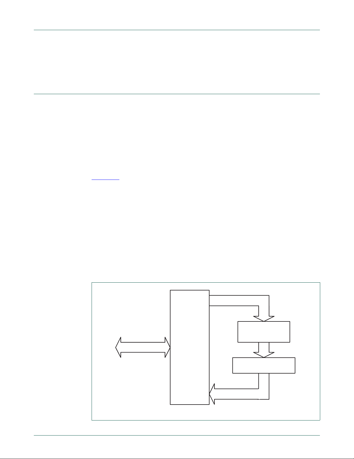
NXP Semiconductors
BUS
INTERFACE
BUFFERS
MEMORY ADDRESS
ARM LOCAL BUS
FLASH MEMORY BANK
the Prefetch and Branch T rail Buffer is taken, a st all of several clocks is needed to load the
Branch Trail Buffer. Subsequently, there will typically be no further instruction fetch delays
until a new and different branch occurs.
3. MAM blocks
The Memory Accelerator Module is divided into several functional blocks:
• A Flash Address Latch and an incrementing function to form prefetch addresses
• A 128-bit Prefetch Buffer and an associated Address latch and comparator
• A 128-bit Branch Trail Buffer and an associated Address latch and comparator
• A 128-bit Data Buffer and an associated Addr ess latch and comparator
• Control logic
• Wait logic
UM10161
Chapter 3: LPC2101/02/03 Memory Acceleration Module (MAM)
Figure 3–6
shows a simplified block diagram of the Memory Accelerator Module data
paths.
In the following descriptions, the term “fetch” applies to an explicit Flash read request from
the ARM. “Pre-fetch” is used to denote a Flash read of instructions beyond the current
processor fetch address.
3.1 Flash memory bank
There is one bank of flash memory on the LPC2101/02/03 MAM.
Flash programming operations are not controlled by the MAM but are handled as a
separate function. A separate boot block in ROM contains flash programming algorithms
that may be called as part of the application program and a loader that may be run to allow
serial programming of the flash memory.
UM10161_4 © NXP B.V. 2009. All rights reserved.
User manual Rev. 4 — 13 May 2009 17 of 292
Fig 6. Simplified block diagram of the Memory Accelerator Module (MAM)

NXP Semiconductors
3.2 Instruction latches and data latches
Code and Data accesses are treated separately by the Memory Accelerator Module.
There is a 128-bit Latch, a 15-bit Address
Latch, and a 15-bit comparator associated with each buffer (prefetch, branch trail, and
data). Each 128-bit latch holds 4 words (4 ARM instructions, or 8 Thumb instructions).
Also associated with each buffer are 32 4:1 Multiplexers that select the requested word
from the 128-bit line.
Each Data access that is not in the Data latch causes a Flash fetch of 4 words of data,
which are captured in the Data latch. This speeds up sequential Data operations, but has
little or no effect on random accesses.
3.3 Flash programming issues
Since the flash memory does not allow accesses du ring pr og ra m m ing and eras e
operations, it is necessary for the MAM to force the CPU to wait if a memory access to a
flash address is requested while the flash module is busy. Under some conditions, this
delay could result in a watchdog time-out. The user will need to be aware of this possibility
and take steps to insure that an un wanted watchdog reset does not cause a system failure
while programming or erasing the flash memory.
UM10161
Chapter 3: LPC2101/02/03 Memory Acceleration Module (MAM)
In order to preclude the possibility of stale data being read from the flash memory, the
LPC2101/02/03 MAM holding latches are automa tically invalidated at the beginning of any
flash programming or erase operation. Any subsequent read from a flash address will
cause a new fetch to be initiated after the flash operation has completed.
4. MAM operating modes
Three modes of operation are defined for the MAM, trading off performance for ease of
predictability:
Mode 0: MAM off. All memory requests result in a Flash read operation (see note 2
below). There are no instruction prefetches.
Mode 1: MAM partially enabled. Sequential instruction accesses are fulfilled from the
holding latches if the data is present. Instruction prefetch is enabled. Non-sequential
instruction accesses initiate Flash read operations (see note 2 below). This means that
all branches cause memory fetches. All data operations cause a Flash read because
buffered data access timing is hard to predict and is very situation dependent.
Mode 2: MAM fully enabled. Any memory request (code or data) for a value that is
contained in one of the corresponding holding latches is fulfilled from the latch.
Instruction prefetch is enabled. Flash read operations are initiated for instruction
prefetch and code or data values not available in the corresponding holding latches.
UM10161_4 © NXP B.V. 2009. All rights reserved.
User manual Rev. 4 — 13 May 2009 18 of 292

NXP Semiconductors
T able 5. MAM Responses to program accesses of various types
Program Memory Request Type MAM Mode
Sequential access, data in latches Initiate Fetch
Sequential access, data not in latches Initiate Fetch Initiate Fetch
Non-sequential access, data in latches Initiate Fetch
Non-sequential access, data not in latches Initiate Fetch Initiate Fetch
[1] Instruction prefetch is enabled in modes 1 and 2.
[2] The MAM actually uses latched data if it is available, but mimics the timing of a Flash read operation. This
Table 6. MAM responses to data accesses of various types
Data Memory Request T ype MAM Mode
Sequential access, data in latches Initiate Fetch
Sequential access, data not in latches Initiate Fetch Initiate Fetch Initiate Fetch
Non-sequential access, data in latches Initiate Fetch
Non-sequential access, data not in latches Initiate Fetch Initiate Fetch Initiate Fetch
UM10161
Chapter 3: LPC2101/02/03 Memory Acceleration Module (MAM)
0 1 2
[2]
Use Latched
[1]
Data
[2]
Initiate Fetch
saves power while resulting in the same execution timing. The MAM can truly be turned off by setting the
fetch timing value in MAMTIM to one clock.
0 1 2
[1]
Initiate Fetch
[1]
Initiate Fetch
Use Latched
Data
[1]
Initiate Fetch
[1][2]
Use Latched
Data
[1]
Initiate Fetch
[1]
Use Latched
Data
[1]
Use Latched
Data
[1]
[1]
[1]
[1]
[1] The MAM actually uses latched data if it is available, but it mimics the timing of a Flash read operation. This
saves power while resulting in the same execution timing. The MAM can truly be turned off by setting the
fetch timing value in MAMTIM to one clock.
5. MAM configuration
After reset the MAM defaults to the disabled state. Software can turn memory access
acceleration on or off at any time. This allows most of an application to be run at the
highest possible performance, while certain functions can be run at a somewhat slower
but more predictable rate if more precise timing is required.
6. Register description
All registers, regardless of size, are on word address boundaries. Details of the registers
appear in the description of each function.
UM10161_4 © NXP B.V. 2009. All rights reserved.
User manual Rev. 4 — 13 May 2009 19 of 292

NXP Semiconductors
Chapter 3: LPC2101/02/03 Memory Acceleration Module (MAM)
T able 7. Summary of MAM registers
Name Description Access Reset
MAMCR Memory Accelerator Module Control Register.
Determines the MAM functional mode, that is, to
what extent the MAM performance enhancements
are enabled. See Table 3–8
MAMTIM Memory Accelerator Module Timing control.
Determines the number of clocks used for Flash
memory fetches (1 to 7 processor clocks).
[1] Reset value reflects the data stored in used bits only. It does not include reserved bits content.
.
7. MAM Control register (MAMCR - 0xE01F C000)
Two configuration bits select the three MAM operating modes, as shown in Table 3–8.
Following Reset, MAM functions are disabled. Changing the MAM operating mode causes
the MAM to invalidate all of the holding latches, resulting in new reads of Flash
information as required.
T able 8. MAM Control Register (MAMCR - address 0xE01F C000) bit description
Bit Symbol Value Description Reset
1:0 MAM_mode
_control
7:2 - - Reserved, user software should not write ones to reserved
00 MAM functions disabled 0
01 MAM functions partially enabled
10 MAM functions fully enabled
11 Reserved. Not to be used in the application.
bits. The value read from a reserved bit is not defined.
UM10161
Address
[1]
value
R/W 0x0 0xE01F C000
R/W 0x07 0xE01F C004
value
NA
8. MAM Timing register (MAMTIM - 0xE01F C004)
The MAM Timing register determines how many CCLK cycles are used to access the
Flash memory. This allows tuning MAM timing to match the processor operating
frequency. Flash access times from 1 clock to 7 clocks are po ssib le . Sing le cloc k Fla sh
accesses would essentially remove the MAM from timing calculations. In this case the
MAM mode may be selected to optimize power usage.
T able 9. MAM Timing register (MAMTIM - address 0xE01F C004) bit description
Bit Symbol Value Description Reset
value
2:0 MAM_fetch_
cycle_timing
UM10161_4 © NXP B.V. 2009. All rights reserved.
User manual Rev. 4 — 13 May 2009 20 of 292
000 0 - Reserved. 07
001 1 - MAM fetch cycles are 1 processor clock (CCLK) in
duration
010 2 - MAM fetch cycles are 2 CCLKs in duration
011 3 - MAM fetch cycles are 3 CCLKs in duration
100 4 - MAM fetch cycles are 4 CCLKs in duration
101 5 - MAM fetch cycles are 5 CCLKs in duration

NXP Semiconductors
T able 9. MAM Timing register (MAMTIM - address 0xE01F C004) bit description
Bit Symbol Value Description Reset
7:3 - - Reserved, user software should not write ones to reserved
9. MAM usage notes
When changing MAM timing, the MAM must first be turned off by writing a zero to
MAMCR. A new value may then be written to MAMTIM. Finally, the MAM may be turned
on again by writing a value (1 or 2) corresponding to the desired operating mode to
MAMCR.
UM10161
Chapter 3: LPC2101/02/03 Memory Acceleration Module (MAM)
value
110 6 - MAM fetch cycles are 6 CCLKs in duration
111 7 - MAM fetch cycles are 7 CCLKs in duration
Warning: These bits set the duration of MAM Flash fetch operations
as listed here. Improper setting of this value may result in incorrect
operation of the device.
NA
bits. The value read from a reserved bit is not defined.
For a system clock slower than 20 MHz, MAMTIM can be 001. For a system clock
between 20 MHz and 40 MHz, flash access time is suggested to be 2 CCLKs, while in
systems with a system clock faster than 40 MHz, 3 CCLKs are proposed. For system
clocks of 60 MHz and above, 4CCLK’s are needed.
Table 10. Suggestions for MAM timing selection
system clock Number of MAM fetch cycles in MAMTIM
< 20 MHz 1 CCLK
20 MHz to 40 MHz 2 CCLK
40 MHz to 60 MHz 3 CCLK
>60 MHz 4 CCLK
UM10161_4 © NXP B.V. 2009. All rights reserved.
User manual Rev. 4 — 13 May 2009 21 of 292

1. Features
2. Description
UM10161
Chapter 4: Vectored Interrupt Controller (VIC)
Rev. 4 — 13 May 2009 User manual
• ARM PrimeCell Vectored Interrupt Controller
• 32 interrupt request inputs
• 16 vectored IRQ interrupts
• 16 priority levels dynamically assigned to interrupt requests
• Software interrupt generation
The Vectored Interrupt Controller (VIC) takes 32 interrupt request inputs and
programmably assigns them into 3 categories, FIQ, vectored IRQ, and non-vectored IRQ.
The programmable assignment scheme means that priorities of interrupts from the
various peripherals can be dynamically assigned and adjusted.
Fast Interrupt reQuest (FIQ) requests have the high est priority. If more than one request is
assigned to FIQ, the VIC ORs the requests to produce the FIQ signal to the ARM
processor. The fastest possible FIQ latency is achieved when only one request is
classified as FIQ because then the FIQ service routine can simply start dealing with that
device. But if more than one request is assigned to the FIQ class, the FIQ service routine
can read a word from the VIC that identifies which FIQ source(s) is (are) requesting an
interrupt.
Vectored IRQs have the midd le priority, but only 16 of the 32 requests can be assigned to
this category. Any of the 32 requests can be assigned to any of the 16 vectored IRQ slots
among which slot 0 has the highest priority and slot 15 has the lowest.
Non-vectored IRQs have the lowest priority.
The VIC ORs the requests from all the vectored and non-vectored IRQs to produce the
IRQ signal to the ARM processor. The IRQ service routine can start by reading a register
from the VIC and jumping there. If any of the vectored IRQs are requesting, the VIC
provides the address of the highest-priority requesting IRQs service routine, otherwise it
provides the address of a default routine that is shared by all the non-vectored IRQs. The
default routine can read another VIC register to see what IRQs are active.
All registers in the VIC are word registers. Byte and halfword reads and write are not
supported.
Additional information on the Vectored Interrupt Controller is available in the ARM
PrimeCell Vectored Interrupt Controller (PL190) documentation.
3. Register description
The VIC implements the registers shown in Table 4–11. More detailed descriptions follow.
UM10161_4 © NXP B.V. 2009. All rights reserved.
User manual Rev. 4 — 13 May 2009 22 of 292

NXP Semiconductors
UM10161
Chapter 4: Vectored Interrupt Controller (VIC)
Table 11. VIC register map
Name Description Access Reset
VICIRQStatus IRQ Status Register. This register reads out the state of
VICFIQStatus FIQ Status Requests. This register reads out the state of
VICRawIntr Raw Interrupt Status Register. This register reads out the
VICIntSelect Interrupt Select Register. This register classifies each of the
VICIntEnable Interrupt Enable Register. This register controls which of the
VICIntEnClr Interrupt Enable Clear Register. This register allows
VICSoftInt Software Interrupt Register. The contents of this register are
VICSoftIntClear Software Interrupt Clear Register. This register allows
VICProtection Protection enable register. This register allows limiting
VICVectAddr Vector Address Register . When an IRQ interrupt occurs, the
VICDefVectAddr Default Vector Address Register. This register holds the
VICVectAddr0 Vector address 0 register. Vector Address Registers 0-15
VICVectAddr1 Vector address 1 register. R/W 0 0xFFFF F104
VICVectAddr2 Vector address 2 register. R/W 0 0xFFFF F108
VICVectAddr3 Vector address 3 register. R/W 0 0xFFFF F10C
VICVectAddr4 Vector address 4 register. R/W 0 0xFFFF F110
VICVectAddr5 Vector address 5 register. R/W 0 0xFFFF F114
VICVectAddr6 Vector address 6 register. R/W 0 0xFFFF F118
VICVectAddr7 Vector address 7 register. R/W 0 0xFFFF F11C
VICVectAddr8 Vector address 8 register. R/W 0 0xFFFF F120
VICVectAddr9 Vector address 9 register. R/W 0 0xFFFF F124
VICVectAddr10 Vector address 10 register. R/W 0 0xFFFF F128
VICVectAddr11 Vector address 11 register. R/W 0 0xFFFF F12C
those interrupt requests that are enabled and classified as
IRQ.
those interrupt requests that are enabled and classified as
FIQ.
state of the 32 interrupt requests / software interrupts,
regardless of enabling or classification.
32 interrupt requests as contributing to FIQ or IRQ.
32 interrupt requests and software interrupts are enabled to
contribute to FIQ or IRQ.
software to clear one or more bits in the Interrupt Enable
register.
ORed with the 32 interrupt requests from various peripheral
functions.
software to clear one or more bits in the Software Interrupt
register.
access to the VIC registers by software running in privileged
mode.
IRQ service routine can read this register and jump to the
value read.
address of the Interrupt Service routine (ISR) for
non-vectored IRQs.
hold the addresses of the Interrupt Service routines (ISRs)
for the 16 vectored IRQ slots.
Address
[1]
value
RO 0 0xFFFF F000
RO 0 0xFFFF F004
RO 0 0xFFFF F008
R/W 0 0xFFFF F00C
R/W 0 0xFFFF F010
WO 0 0xFFFF F014
R/W 0 0xFFFF F018
WO 0 0xFFFF F01C
R/W 0 0xFFFF F020
R/W 0 0xFFFF F030
R/W 0 0xFFFF F034
R/W 0 0xFFFF F100
UM10161_4 © NXP B.V. 2009. All rights reserved.
User manual Rev. 4 — 13 May 2009 23 of 292

NXP Semiconductors
UM10161
Chapter 4: Vectored Interrupt Controller (VIC)
Table 11. VIC register map
Name Description Access Reset
value
VICVectAddr12 Vector address 12 register. R/W 0 0xFFFF F130
VICVectAddr13 Vector address 13 register. R/W 0 0xFFFF F134
VICVectAddr14 Vector address 14 register. R/W 0 0xFFFF F138
VICVectAddr15 Vector address 15 register. R/W 0 0xFFFF F13C
VICVectCntl0 Vector control 0 register. Vector Control Registers 0-15 each
control one of the 16 vectored IRQ slots. Slot 0 has the
highest priority and slot 15 the lowest.
VICVectCn tl 1 Vector control 1 regi ster. R/W 0 0xFFFF F204
VICVectCn tl 2 Vector control 2 regi ster. R/W 0 0xFFFF F208
VICVectCn tl 3 Vector control 3 regi ster. R/W 0 0xFFFF F20C
VICVectCn tl 4 Vector control 4 regi ster. R/W 0 0xFFFF F210
VICVectCn tl 5 Vector control 5 regi ster. R/W 0 0xFFFF F214
VICVectCn tl 6 Vector control 6 regi ster. R/W 0 0xFFFF F218
VICVectCn tl 7 Vector control 7 regi ster. R/W 0 0xFFFF F21C
VICVectCn tl 8 Vector control 8 regi ster. R/W 0 0xFFFF F220
VICVectCn tl 9 Vector control 9 regi ster. R/W 0 0xFFFF F224
VICVectCntl10 Vector control 10 register. R/W 0 0xFFFF F228
VICVectCntl11 Vector control 11 register. R/W 0 0xFFFF F22C
VICVectCntl12 Vector control 12 register. R/W 0 0xFFFF F230
VICVectCntl13 Vector control 13 register. R/W 0 0xFFFF F234
VICVectCntl14 Vector control 14 register. R/W 0 0xFFFF F238
VICVectCntl15 Vector control 15 register. R/W 0 0xFFFF F23C
R/W 0 0xFFFF F200
Address
[1]
[1] Reset value reflects the data stored in used bits only. It does not include reserved bits content.
4. VIC registers
The following section describes the VIC registers in the order in which they are used in the
VIC logic, from those closest to the interrupt request inputs to those most abstracted for
use by software. For most people, this is also the best order to read about the registers
when learning the VIC.
4.1 Software Interrupt register (VICSoftInt - 0xFFFF F018)
The contents of this register are ORed with the 32 interrupt requests from the various
peripherals, before any other logic is applied.
Table 12. Software Interrupt register (VICSoftInt - address 0xFFFF F018) bit allocation
Reset value: 0x0000 0000
Bit 31 30 29 28 27 26 25 24
Symbol ----TIMER3TIMER2-Access R/W R/W R/W R/W R/W R/W R/W R/W
UM10161_4 © NXP B.V. 2009. All rights reserved.
User manual Rev. 4 — 13 May 2009 24 of 292

NXP Semiconductors
UM10161
Chapter 4: Vectored Interrupt Controller (VIC)
Bit 23 22 21 20 19 18 17 16
Symbol ----I2C1AD0-EINT2
Access R/W R/W R/W R/W R/W R/W R/W R/W
Bit 15 14 13 12 11 10 9 8
Symbol EINT1 EINT0 RTC PLL SSP/SPI1 SPI0 I2C0 -
Access R/W R/W R/W R/W R/W R/W R/W R/W
Bit 7 6 5 4 3 2 1 0
Symbol UART1 UART0 TIMER1 TIMER0 ARMCore1 ARMCore0 - WDT
Access R/W R/W R/W R/W R/W R/W R/W R/W
Table 13. Software Interrupt register (VICSoftInt - address 0xFFFF F018) bit description
Bit Symbol Value Description Reset
value
31:0 See VICSoftInt
bit allocation
table.
0 Do not force the interrupt request with this bit number. Writing
zeroes to bits in VICSoftInt has no effect, see VICSoftIntClear
(Section 4–4.2
).
0
1 Force the interrupt request with this bit number.
4.2 Software Interrupt Clear register (VICSoftIntClear - 0xFFFF F01C)
This register allows software to clear one or more bits in the Softwar e Interrupt register,
without having to first read it.
Table 14. Software Interrupt Clear register (VICSoftIntClear - address 0xFFFF F01C) bit allocation
Reset value: 0x0000 0000
Bit 31 30 29 28 27 26 25 24
Symbol ----TIMER3TIMER2-Access WO WO WO WO WO WO WO WO
Bit 23 22 21 20 19 18 17 16
Symbol ----I2C1AD0-EINT2
Access WO WO WO WO WO WO WO WO
Bit 15 14 13 12 11 10 9 8
Symbol EINT1 EINT0 RTC PLL SSP/SPI1 SPI0 I2C0 -
Access WO WO WO WO WO WO WO WO
Bit 7 6 5 4 3 2 1 0
Symbol UART1 UART0 TIMER1 TIMER0 ARMCore1 ARMCore0 - WDT
Access WO WO WO WO WO WO WO WO
Table 15. Software Interrupt Clear register (VICSoftIntClear - address 0xFFFF F0 1C) bit desc ription
Bit Symbol Value Description Reset
value
31:0 See
VICSoftIntClea
r bit allocation
table.
UM10161_4 © NXP B.V. 2009. All rights reserved.
User manual Rev. 4 — 13 May 2009 25 of 292
0 Writing a 0 leave s the corresponding bit in VICSoftInt unchanged. 0
1 Writing a 1 clears the corresponding bit in the Software Interrupt
register, thus releasing the forcing of this request.

NXP Semiconductors
UM10161
Chapter 4: Vectored Interrupt Controller (VIC)
4.3 Raw Interrupt status register (VICRawIntr - 0xFFFF F008)
This is a read only register. This register reads out the state of the 32 interrupt requests
and software interrupts, regardless of enabling or classification.
Table 16. Raw Interrupt status register (VICRawIntr - address 0xFFFF F008) bit allocation
Reset value: 0x0000 0000
Bit 31 30 29 28 27 26 25 24
Symbol ----TIMER3TIMER2-Access RO RO RO RO RO RO RO RO
Bit 23 22 21 20 19 18 17 16
Symbol ----I2C1AD0-EINT2
Access RO RO RO RO RO RO RO RO
Bit 15 14 13 12 11 10 9 8
Symbol EINT1 EINT0 RTC PLL SSP/SPI1 SPI0 I2C0 -
Access RO RO RO RO RO RO RO RO
Bit 7 6 5 4 3 2 1 0
Symbol UART1 UART0 TIMER1 TIMER0 ARMCore1 ARMCore0 - WDT
Access RO RO RO RO RO RO RO RO
Table 17. Raw Interrupt status register (VICRawIntr - address 0xFFFF F008) bit description
Bit Symbol Value Description Reset
value
31:0 See
VICRawIntr bit
allocation
table.
0 Neither the hardware nor software interrupt request with this bit
number are asserted.
1 The hardware or software interrupt request with this bit number is
asserted.
0
4.4 Interrupt Enable register (VICIntEnable - 0xFFFF F010)
This is a read/write accessible register. This register controls which of the 32 interrupt
requests and software interrupts contribute to FIQ or IRQ.
Table 18. Interrupt Enable register (VICIntEnable - address 0xFFFF F010) bit allocation
Reset value: 0x0000 0000
Bit 31 30 29 28 27 26 25 24
Symbol ----TIMER3TIMER2-Access R/W R/W R/W R/W R/W R/W R/W R/W
Bit 23 22 21 20 19 18 17 16
Symbol ----I2C1AD0-EINT2
Access R/W R/W R/W R/W R/W R/W R/W R/W
Bit 15 14 13 12 11 10 9 8
Symbol EINT1 EINT0 RTC PLL SSP/SPI1 SPI0 I2C0 -
Access R/W R/W R/W R/W R/W R/W R/W R/W
Bit 7 6 5 4 3 2 1 0
Symbol UART1 UART0 TIMER1 TIMER0 ARMCore1 ARMCore0 - WDT
Access R/W R/W R/W R/W R/W R/W R/W R/W
UM10161_4 © NXP B.V. 2009. All rights reserved.
User manual Rev. 4 — 13 May 2009 26 of 292

NXP Semiconductors
UM10161
Chapter 4: Vectored Interrupt Controller (VIC)
Table 19. Interrupt Enable register (VICIntEnable - address 0xFFFF F010) bit description
Bit Symbol Description Reset
value
31:0 See
VICIntEnable
bit allocation
table.
When this register is read, 1s indicate interrupt requests or software interrupts
that are enabled to contribute to FIQ or IRQ.
When this register is written, ones enable interrupt requests or software
interrupts to contribute to FIQ or IRQ, zeroes have no effect. See Section 4–4.5
0
“Interrupt Enable Clear register (VICIntEnClear - 0xFFFF F014)” on page 27
and Table 4–21 below for how to disable interrupts.
4.5 Interrupt Enable Clear register (VICIntEnClear - 0xFFFF F014)
This is a write only register. This register allows software to clear one or more bits in the
Interrupt Enable register (see Section 4–4.4 “
0xFFFF F010)” on page 26), without having to first read it.
Table 20. Software Interrupt Clear register (VICIntEnClear - address 0xFFFF F014) bit allocation
Reset value: 0x0000 0000
Bit 31 30 29 28 27 26 25 24
Symbol ----TIMER3TIMER2-Access WO WO WO WO WO WO WO WO
Bit 23 22 21 20 19 18 17 16
Symbol ----I2C1AD0-EINT2
Access WO WO WO WO WO WO WO WO
Bit 15 14 13 12 11 10 9 8
Symbol EINT1 EINT0 RTC PLL SSP/SPI1 SPI0 I2C0 -
Access WO WO WO WO WO WO WO WO
Bit 7 6 5 4 3 2 1 0
Symbol UART1 UART0 TIMER1 TIMER0 ARMCore1 ARMCore0 - WDT
Access WO WO WO WO WO WO WO WO
Interrupt Enable register (VICIntEnable -
Table 21. Software Interrupt Clear register (VICIntEnClear - address 0xFFFF F014) bit description
Bit Symbol Value Description Reset
value
31:0 See
VICIntEnClear
bit allocation
table.
0 Writing a 0 leaves the corresponding bit in VICIntEnable
unchanged.
1 Writing a 1 clears the corresponding bit in the Interrupt Enable
register, thus disabling interrupts for this request.
0
4.6 Interrupt Select register (VICIntSelect - 0xFFFF F00C)
This is a read/write accessible register. This register classifies each of the 32 interrupt
requests as contributing to FIQ or IRQ.
Table 22. Interrupt Select register (VICIntSelect - address 0xFFFF F00C) bit allocation
Reset value: 0x0000 0000
Bit 31 30 29 28 27 26 25 24
Symbol ----TIMER3TIMER2-Access R/W R/W R/W R/W R/W R/W R/W R/W
UM10161_4 © NXP B.V. 2009. All rights reserved.
User manual Rev. 4 — 13 May 2009 27 of 292

NXP Semiconductors
UM10161
Chapter 4: Vectored Interrupt Controller (VIC)
Bit 23 22 21 20 19 18 17 16
Symbol ----I2C1AD0-EINT2
Access R/W R/W R/W R/W R/W R/W R/W R/W
Bit 15 14 13 12 11 10 9 8
Symbol EINT1 EINT0 RTC PLL SSP/SPI1 SPI0 I2C0 -
Access R/W R/W R/W R/W R/W R/W R/W R/W
Bit 7 6 5 4 3 2 1 0
Symbol UART1 UART0 TIMER1 TIMER0 ARMCore1 ARMCore0 - WDT
Access R/W R/W R/W R/W R/W R/W R/W R/W
Table 23. Interrupt Select register (VICIntSelect - address 0xFFFF F00C) bit description
Bit Symbol Value Description Reset
value
31:0 See
VICIntSelect
bit allocation
table.
0 The interrupt reque st with this bit number is assigned to the IRQ
category.
1 The interrupt reque st with this bit number is assigned to the FIQ
category.
0
4.7 IRQ Status register (VICIRQStatus - 0xFFFF F000)
This is a read only register. This register reads out the state of those interrupt requests
that are enabled and classified as IRQ. It does not differentiate between vectored and
non-vectored IRQs.
Table 24. IRQ Status register (VICIRQStatus - address 0xFFFF F000) bit allocation
Reset value: 0x0000 0000
Bit 31 30 29 28 27 26 25 24
Symbol ----TIMER3TIMER2-Access RO RO RO RO RO RO RO RO
Bit 23 22 21 20 19 18 17 16
Symbol ----I2C1AD0-EINT2
Access RO RO RO RO RO RO RO RO
Bit 15 14 13 12 11 10 9 8
Symbol EINT1 EINT0 RTC PLL SSP/SPI1 SPI0 I2C0 -
Access RO RO RO RO RO RO RO RO
Bit 7 6 5 4 3 2 1 0
Symbol UART1 UART0 TIMER1 TIMER0 ARMCore1 ARMCore0 - WDT
Access RO RO RO RO RO RO RO RO
Table 25. IRQ Status register (VICIRQStatus - address 0xFFFF F000) bit descrip tion
Bit Symbol Description Reset
value
31:0 See
VICIRQStatus
A bit read as 1 indicates a corresponding interrupt request being enabled,
classified as IRQ, and asserted
0
bit allocation
table.
UM10161_4 © NXP B.V. 2009. All rights reserved.
User manual Rev. 4 — 13 May 2009 28 of 292

NXP Semiconductors
UM10161
Chapter 4: Vectored Interrupt Controller (VIC)
4.8 FIQ Status register (VICFIQStatus - 0xFFFF F004)
This is a read only register. This register reads out the state of those interrupt requests
that are enabled and classified as FIQ. If more than one request is classified as FIQ, the
FIQ service routine can read this register to see which request(s) is (are) active.
Table 26. FIQ Status register (VICFIQStatus - address 0xFFFF F004) bit allocation
Reset value: 0x0000 0000
Bit 31 30 29 28 27 26 25 24
Symbol ----TIMER3TIMER2-Access RO RO RO RO RO RO RO RO
Bit 23 22 21 20 19 18 17 16
Symbol ----I2C1AD0-EINT2
Access RO RO RO RO RO RO RO RO
Bit 15 14 13 12 11 10 9 8
Symbol EINT1 EINT0 RTC PLL SSP/SPI1 SPI0 I2C0 -0
Access RO RO RO RO RO RO RO RO
Bit 7 6 5 4 3 2 1 0
Symbol UART1 UART0 TIMER1 TIMER0 ARMCore1 ARMCore0 - WDT
Access RO RO RO RO RO RO RO RO
Table 27. FIQ Status register (VICFIQStatus - address 0xFFFF F004) bit description
Bit Symbol Description Reset
31:0 See
VICFIQStatus
bit allocation
table.
A bit read as 1 indicates a corresponding interrupt request being enabled,
classified as FIQ, and asserted
value
0
4.9 Vector Control registers 0-15 (VICVectCntl0-15 - 0xFFFF F200-23C)
These are a read/write accessible registers. Each of these registers controls one of the 16
vectored IRQ slots. Slot 0 has the highest priority and slot 15 the lowest. Note that
disabling a vectored IRQ slot in one of the VICVectCntl registers does not disable the
interrupt itself, the interrupt is simply changed to the non-vectored form.
Table 28. Vector Control registers 0-15 (VICVectCntl0-15 - 0xFFFF F200-23C) bit description
Bit Symbol Description Reset
4:0 int_request/
sw_int_assig
5 IRQslot_en When 1, this vectored IRQ slot is enabled, and can produce a unique ISR
31:6 - Reserved, user software should not write ones to reserved bits. The value read
The number of the interrupt request or software interrupt assigned to this
vectored IRQ slot. As a matter of good programming practice, software should
not assign the same interrupt number to more than one enabled vectored IRQ
slot. But if this does occur, the lower numbered slot will be used when the
interrupt request or software interrupt is enabled, classified as IRQ, and
asserted.
address when its assigned interrupt request or software interrupt is enabled,
classified as IRQ, and asserted.
from a reserved bit is not defined.
value
0
0
NA
UM10161_4 © NXP B.V. 2009. All rights reserved.
User manual Rev. 4 — 13 May 2009 29 of 292

NXP Semiconductors
UM10161
Chapter 4: Vectored Interrupt Controller (VIC)
4.10 Vector Address registers 0-15 (VICVectAddr0-15 - 0xFFFF F100-13C)
These are a read/write accessible registers. These registers ho ld the addresses of the
Interrupt Service routines (ISRs) for the 16 vectored IRQ slots.
Table 29. Vector Address registers (VICVectAddr0-15 - addresses 0xFFFF F100-13C) bit description
Bit Symbol Description Reset value
31:0 IRQ_vector When one or more interrupt request or software interrupt is (are) enabled,
classified as IRQ, asserted, and assigned to an enabled vectored IRQ slot,
the value from this register for the highest-priority such slot will be provided
when the IRQ service routine reads the Vector Address register -VICVectAddr
(Section 4–4.10
).
0x0000 0000
4.11 Default Vector Address register (VICDefVectAddr - 0xFFFF F034)
This is a read/write accessible register. This register holds the address of the Interrupt
Service routine (ISR) for non-vectored IRQs.
Table 30. Default Vector Address register (VICDefVectAddr - address 0xFFFF F034) bit description
Bit Symbol Description Reset value
31:0 IRQ_vector When an IRQ service routine reads the Vector Address register
0x0000 0000
(VICVectAddr), and no IRQ slot responds as described above, this address is
returned.
4.12 Vector Address register (VICVectAddr - 0xFFFF F030)
This is a read/write accessible register. When an IRQ interrupt occurs, the IRQ service
routine can read this register and jump to the value read.
Table 31. Vector Address register (VICVectAddr - address 0xFFFF F030) bit description
Bit Symbol Description Reset value
31:0 IRQ_vector If any of the interrupt requests or software interrupts that are assigned to a
0x0000 0000
vectored IRQ slot is (are) enabled, classified as IRQ, and asserted, reading
from this register returns the address in the Vector Address Register for the
highest-priority such slot (lowest-numbered) such slot. Otherwise it returns the
address in the Default Vector Address Register.
Writing to this register does not set the value for future reads from it. Rather,
this register should be written near the end of an ISR, to update the priority
hardware.
4.13 Protection Enable register (VICProtection - 0xFFFF F020)
This is a read/write accessible register. It controls access to the VIC registers by software
running in User mode.
Table 32. Protection Enable register (VICProtection - address 0xFFFF F020) bit description
Bit Symbol Value Description Reset
0 VIC_access 0 VIC registers can be accessed in User or privileged mode. 0
31:1 - Reserved, user software should not write ones to reserved bits. The
value
1 Th e VIC registers can only be accessed in privileged mode.
NA
value read from a reserved bit is not defined.
UM10161_4 © NXP B.V. 2009. All rights reserved.
User manual Rev. 4 — 13 May 2009 30 of 292
Loading...