


June 1999
MF10
Universal Monolithic Dual Switched Capacitor Filter
General Description
The MF10 consists of 2 independent and extremely easy to use, general purpose CMOS active filter building blocks. Each block, together with an external clock and 3 to 4 resistors, can produce various 2nd order functions. Each building block has 3 output pins. One of the outputs can be configured to perform either an allpass, highpass or a notch function; the remaining 2 output pins perform lowpass and bandpass functions. The center frequency of the lowpass and bandpass 2nd order functions can be either directly dependent on the clock frequency, or they can depend on both clock frequency and external resistor ratios. The center frequency of the notch and allpass functions is directly dependent on the clock frequency, while the highpass center frequency depends on both resistor ratio and clock. Up to 4th order functions can be performed by cascading the two 2nd order building blocks of the MF10; higher than 4th order functions can be obtained by cascading MF10 packages.
Any of the classical filter configurations (such as Butterworth, Bessel, Cauer and Chebyshev) can be formed.
For pin-compatible device with improved performance refer to LMF100 datasheet.
Features
nEasy to use
nClock to center frequency ratio accuracy ±0.6%
nFilter cutoff frequency stability directly dependent on external clock quality
nLow sensitivity to external component variation
nSeparate highpass (or notch or allpass), bandpass, lowpass outputs
nfO x Q range up to 200 kHz
nOperation up to 30 kHz
n20-pin 0.3" wide Dual-In-Line package
n20-pin Surface Mount (SO) wide-body package
System Block Diagram
DS010399-1
Package in 20 pin molded wide body surface mount and 20 pin molded DIP.
Filter Capacitor Switched Dual Monolithic Universal MF10
© 1999 National Semiconductor Corporation |
DS010399 |
www.national.com |

Absolute Maximum Ratings (Note 1)
If Military/Aerospace specified devices are required, please contact the National Semiconductor Sales Office/ Distributors for availability and specifications.
Supply Voltage (V+ − V − ) |
14V |
Voltage at Any Pin |
V+ + 0.3V |
|
V− − 0.3V |
Input Current at Any Pin (Note 2) |
5 mA |
Package Input Current (Note 2) |
20 mA |
Power Dissipation (Note 3) |
500 mW |
Storage Temperature |
150ÊC |
ESD Susceptability (Note 11) |
2000V |
Soldering Information |
|
N Package: 10 sec |
260ÊC |
SO Package: |
|
Vapor Phase (60 Sec.) |
215ÊC |
Infrared (15 Sec.) |
220ÊC |
See AN-450 ªSurface Mounting Methods and Their Effect on Product Reliabilityº (Appendix D) for other methods of soldering surface mount devices.
Operating Ratings (Note 1)
Temperature Range |
TMIN ≤ TA ≤ TMAX |
MF10ACN, MF10CCN |
0ÊC ≤ TA ≤ 70ÊC |
MF10CCWM |
0ÊC ≤ TA ≤ 70ÊC |
Electrical Characteristics
V+ = +5.00V and V− = −5.00V unless otherwise specified. Boldface limits apply for TMIN to TMAX; all other limits TA = TJ = 25ÊC.
|
|
|
|
|
|
|
|
MF10ACN, MF10CCN, |
|
|
||
|
|
|
|
|
|
|
|
|
MF10CCWM |
|
|
|
|
|
|
|
|
|
|
|
|
|
|
|
|
Symbol |
Parameter |
|
Conditions |
Typical |
|
Tested |
|
Design |
Units |
|||
|
|
|
|
|
|
|
(Note 8) |
|
Limit |
|
Limit |
|
|
|
|
|
|
|
|
|
|
(Note 9) |
|
(Note 10) |
|
|
|
|
|
|
|
|
|
|
|
|
|
|
V+ − V − |
Supply Voltage |
|
Min |
|
|
|
|
|
|
|
9 |
V |
|
|
|
Max |
|
|
|
|
|
|
|
14 |
V |
|
|
|
|
|
|
|
|
|
|
|
|
|
IS |
Maximum Supply |
|
Clock Applied to Pins 10 & 11 |
8 |
|
12 |
|
12 |
mA |
|||
|
Current |
|
No Input Signal |
|
|
|
|
|
|
|
||
|
|
|
|
|
|
|
|
|
|
|
|
|
fO |
Center Frequency |
|
Min |
fO x Q < 200 kHz |
|
0.1 |
|
|
|
0.2 |
Hz |
|
|
Range |
|
Max |
|
|
|
30 |
|
|
|
20 |
kHz |
|
|
|
|
|
|
|
|
|
|
|
|
|
fCLK |
Clock Frequency |
|
Min |
|
|
|
5.0 |
|
|
|
10 |
Hz |
|
Range |
|
Max |
|
|
|
1.5 |
|
|
|
1.0 |
MHz |
|
|
|
|
|
|
|
|
|
|
|
|
|
fCLK/fO |
50:1 Clock to |
|
MF10C |
Q = 10 |
|
Vpin12 = 5V |
±0.2 |
|
±1.5 |
|
± 1.5 |
|
|
Center Frequency |
|
|
Mode 1 |
|
fCLK = 250 KHz |
|
|
% |
|||
|
Ratio Deviation |
|
|
|
|
|
|
|
|
|
|
|
fCLK/fO |
100:1 Clock to |
|
MF10C |
Q = 10 |
|
Vpin12 = 0V |
±0.2 |
|
±1.5 |
|
± 1.5 |
|
|
Center Frequency |
|
|
Mode 1 |
|
fCLK = 500 kHz |
|
|
% |
|||
|
Ratio Deviation |
|
|
|
|
|
|
|
|
|
|
|
|
|
|
|
|
|
|
|
|
|
|
|
|
|
Clock Feedthrough |
|
Q = 10 |
|
10 |
|
|
|
|
mV |
||
|
|
|
|
Mode 1 |
|
|
|
|
|
|||
|
|
|
|
|
|
|
|
|
|
|
||
|
|
|
|
|
|
|
|
|
|
|
|
|
|
Q Error (MAX) |
|
Q = 10 |
|
Vpin12 = 5V |
±2 |
|
±6 |
|
± 6 |
% |
|
|
(Note 4) |
|
Mode 1 |
|
fCLK = 250 kHz |
|
|
|
|
|
|
|
|
|
|
|
|
|
Vpin12 = 0V |
±2 |
|
±6 |
|
± 6 |
% |
|
|
|
|
|
|
fCLK = 500 kHz |
|
|
|
|
|
|
HOLP |
DC Lowpass Gain |
|
Mode 1 R1 = R2 = 10k |
|
0 |
|
±0.2 |
|
± 0.2 |
dB |
||
VOS1 |
DC Offset Voltage (Note 5) |
|
|
|
|
±5.0 |
|
±20 |
|
± 20 |
mV |
|
VOS2 |
DC Offset Voltage |
|
Min |
Vpin12 = +5V |
|
SA/B = V+ |
−150 |
|
−185 |
|
−185 |
mV |
|
(Note 5) |
|
Max |
(fCLK/fO = 50) |
|
|
|
|
−85 |
|
−85 |
|
|
|
|
Min |
Vpin12 = +5V |
|
SA/B = V− |
−70 |
|
|
|
|
mV |
|
|
|
Max |
(fCLK/fO = 50) |
|
|
|
|
|
|
|
|
VOS3 |
DC Offset Voltage |
|
Min |
Vpin12 = +5V |
|
All Modes |
−70 |
|
−100 |
|
−100 |
mV |
|
(Note 5) |
|
Max |
(fCLK/fO = 50) |
|
|
|
|
−20 |
|
−20 |
|
VOS2 |
DC Offset Voltage |
|
Vpin12 = 0V |
|
SA/B = V+ |
−300 |
|
|
|
|
mV |
|
|
(Note 5) |
|
(fCLK/fO = 100) |
|
|
|
|
|
|
|
|
|
|
|
|
|
Vpin12 = 0V |
|
SA/B = V− |
−140 |
|
|
|
|
mV |
|
|
|
|
(fCLK/fO = 100) |
|
|
|
|
|
|
|
|
VOS3 |
DC Offset Voltage |
|
Vpin12 = 0V |
|
All Modes |
−140 |
|
|
|
|
mV |
|
|
(Note 5) |
|
(fCLK/fO = 100) |
|
|
|
|
|
|
|
|
|
VOUT |
Minimum Output |
|
BP, LP Pins |
RL = 5k |
|
±4.25 |
|
±3.8 |
|
± 3.8 |
V |
|
|
Voltage Swing |
|
N/AP/HP Pin |
RL = 3.5k |
|
±4.25 |
|
±3.8 |
|
± 3.8 |
V |
|
GBW |
Op Amp Gain BW Product |
|
|
|
|
2.5 |
|
|
|
|
MHz |
|
|
|
|
|
|
|
|
|
|
|
|
|
|
SR |
Op Amp Slew Rate |
|
|
|
|
7 |
|
|
|
|
V/µs |
|
|
|
|
|
|
|
|
|
|
|
|
|
|
www.national.com |
2 |

Electrical Characteristics (Continued)
V+ = +5.00V and V− = −5.00V unless otherwise specified. Boldface limits apply for TMIN to TMAX; all other limits TA = TJ = 25ÊC.
|
|
|
|
|
|
MF10ACN, MF10CCN, |
|
|
||
|
|
|
|
|
|
|
MF10CCWM |
|
|
|
|
|
|
|
|
|
|
|
|
|
|
Symbol |
Parameter |
|
Conditions |
Typical |
|
Tested |
|
Design |
Units |
|
|
|
|
|
|
(Note 8) |
|
Limit |
|
Limit |
|
|
|
|
|
|
|
|
(Note 9) |
|
(Note 10) |
|
|
|
|
|
|
|
|
|
|
|
|
|
Dynamic |
|
Vpin12 = +5V |
83 |
|
|
|
|
dB |
|
|
Range(Note 6) |
|
(fCLK/fO = 50) |
|
|
|
|
|||
|
|
|
|
|
|
|
|
|||
|
|
|
|
Vpin12 = 0V |
80 |
|
|
|
|
dB |
|
|
|
|
(fCLK/fO = 100) |
|
|
|
|
|
|
ISC |
Maximum Output |
|
Source |
|
20 |
|
|
|
|
mA |
|
Short |
|
|
|
|
|
|
|
|
|
|
|
|
|
|
|
|
|
|
|
|
|
Circuit Current |
|
Sink |
|
3.0 |
|
|
|
|
mA |
|
(Note 7) |
|
|
|
|
|
|
|
|
|
|
|
|
|
|
|
|
|
|
|
|
Logic Input Characteristics
Boldface limits apply for TMIN to TMAX; all other limits TA = TJ = 25ÊC
|
|
|
|
|
|
|
|
MF10ACN, MF10CCN, |
|
|
||
|
|
|
|
|
|
|
|
|
MF10CCWM |
|
|
|
|
|
|
|
|
|
|
|
|
|
|||
|
Parameter |
Conditions |
Typical |
|
Tested |
|
Design |
Units |
||||
|
|
|
|
|
|
|
(Note 8) |
|
Limit |
|
Limit |
|
|
|
|
|
|
|
|
|
|
(Note 9) |
|
(Note 10) |
|
|
|
|
|
|
|
|
|
|
|
|
|
|
CMOS Clock |
|
Min Logical ª1º |
+ |
− |
|
= −5V, |
|
|
+3.0 |
|
+3.0 |
V |
|
V = +5V, V |
|
|
|
|
|
||||||
Input Voltage |
|
Max Logical ª0º |
VLSh = 0V |
|
|
|
|
|
−3.0 |
|
−3.0 |
V |
|
|
Min Logical ª1º |
+ |
|
− |
= 0V, |
|
|
+8.0 |
|
+8.0 |
V |
|
|
V = +10V, V |
|
|
|
|
||||||
|
|
Max Logical ª0º |
VLSh = +5V |
|
|
|
|
|
+2.0 |
|
+2.0 |
V |
TTL Clock |
|
Min Logical ª1º |
+ |
− |
|
= −5V, |
|
|
+2.0 |
|
+2.0 |
V |
|
V = +5V, V |
|
|
|
|
|
||||||
Input Voltage |
|
Max Logical ª0º |
VLSh = 0V |
|
|
|
|
|
+0.8 |
|
+0.8 |
V |
|
|
Min Logical ª1º |
+ |
|
− |
= 0V, |
|
|
+2.0 |
|
+2.0 |
V |
|
|
V = +10V, V |
|
|
|
|
||||||
|
|
Max Logical ª0º |
VLSh = +5V |
|
|
|
|
|
+0.8 |
|
+0.8 |
V |
Note 1: Absolute Maximum Ratings indicate limits beyond which damage to the device may occur. DC and AC electrical specifications do not apply when operating the device beyond its specified operating conditions.
Note 2: When the input voltage (VIN) at any pin exceeds the power supply rails (VIN < V− or VIN > V+) the absolute value of current at that pin should be limited to 5 mA or less. The 20 mA package input current limits the number of pins that can exceed the power supply boundaries with a 5 mA current limit to four.
Note 3: The maximum power dissipation must be derated at elevated temperatures and is dictated by TJMAX, θJA, and the ambient temperature, TA. The maximum allowable power dissipation at any temperature is PD = (TJMAX − T A)/θJA or the number given in the Absolute Maximum Ratings, whichever is lower. For this device, TJMAX = 125ÊC, and the typical junction-to-ambient thermal resistance of the MF10ACN/CCN when board mounted is 55ÊC/W. For the MF10AJ/CCJ, this number increases to 95ÊC/W and for the MF10ACWM/CCWM this number is 66ÊC/W.
Note 4: The accuracy of the Q value is a function of the center frequency (fO). This is illustrated in the curves under the heading ªTypical Performance Characteristicsº.
Note 5: VOS1, VOS2, and VOS3 refer to the internal offsets as discussed in the Applications Information Section 3.4.
Note 6: For ±5V supplies the dynamic range is referenced to 2.82V rms (4V peak) where the wideband noise over a 20 kHz bandwidth is typically 200 µV rms for the MF10 with a 50:1 CLK ratio and 280 µV rms for the MF10 with a 100:1 CLK ratio.
Note 7: The short circuit source current is measured by forcing the output that is being tested to its maximum positive voltage swing and then shorting that output to the negative supply. The short circuit sink current is measured by forcing the output that is being tested to its maximum negative voltage swing and then shorting that output to the positive supply. These are the worst case conditions.
Note 8: Typicals are at 25ÊC and represent most likely parametric norm.
Note 9: Tested limits are guaranteed to National's AOQL (Average Outgoing Quality Level).
Note 10: Design limits are guaranteed but not 100% tested. These limits are not used to calculate outgoing quality levels.
Note 11: Human body model, 100 pF discharged through a 1.5 kΩ resistor.
3 |
www.national.com |
Typical Performance Characteristics
Power Supply Current |
Positive Output Voltage Swing |
Negative Output Voltage |
|
vs Power Supply Voltage |
vs Load Resistance |
||
Swing vs Load |
|||
|
(N/AP/HP Output) |
||
|
Resistance (N/AP/HP Output) |
||
|
|
Negative Output Swing vs Temperature
Q Deviation vs
Temperature
DS010399-34
|
DS010399-35 |
|
DS010399-36 |
Positive Output Swing |
Crosstalk vs Clock |
vs Temperature |
Frequency |
DS010399-37 DS010399-38 DS010399-39
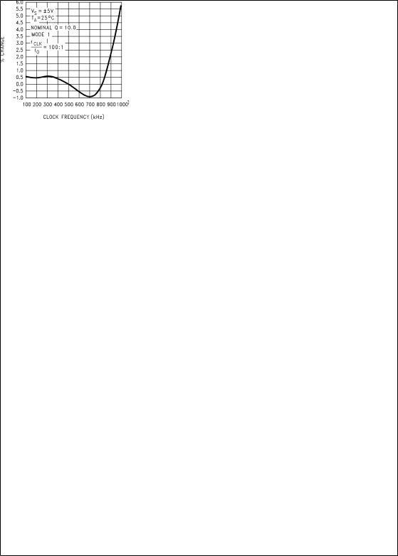
Q Deviation vs |
Q Deviation vs |
Temperature |
Clock Frequency |
DS010399-40 |
DS010399-41 |
DS010399-42 |
www.national.com |
4 |
Typical Performance Characteristics (Continued)
Q Deviation vs |
fCLK/fO Deviation |
fCLK/fO Deviation |
Clock Frequency |
vs Temperature |
vs Temperature |
DS010399-43 DS010399-44 DS010399-45
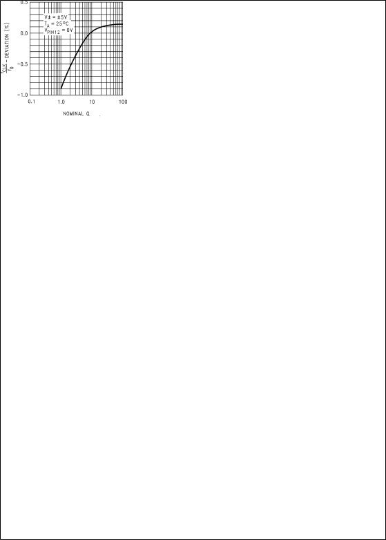
fCLK/fO Deviation |
fCLK/fO Deviation |
Deviation of fCLK/fO |
vs Clock Frequency |
vs Clock Frequency |
vs Nominal Q |
DS010399-46 |
DS010399-47 |
DS010399-48 |
Deviation of fCLK/fO vs Nominal Q
DS010399-49
5 |
www.national.com |

Pin Descriptions
LP(1,20), BP(2,19), The second order lowpass, bandpass N/AP/HP(3,18) and notch/allpass/highpass outputs.
These outputs can typically sink 1.5 mA and source 3 mA. Each output typically swings to within 1V of each supply.
INV(4,17) |
The inverting input of the summing |
|||
|
op-amp of each filter. These are high |
|||
|
impedance |
inputs, |
but |
the |
|
non-inverting input is internally tied to |
|||
|
AGND, making INVA and INVB behave |
|||
|
like summing junctions (low imped- |
|||
|
ance, current inputs). |
|
|
|
S1(5,16) |
S1 is a signal input pin used in the all- |
|||
|
pass filter configurations (see modes 4 |
|||
|
and 5). The pin should be driven with a |
|||
|
source impedance of less than 1 kΩ. If |
|||
|
S1 is not driven with a signal it should |
|||
|
be tied to AGND (mid-supply). |
|
||
SA/B(6) |
This pin activates a switch that con- |
|||
|
nects one of the inputs of each filter's |
|||
|
second summer to either AGND (SA/B |
|||
|
tied to V− ) or to the lowpass (LP) out- |
|||
|
put (SA/B tied to V+). This offers the |
|||
|
flexibility needed for configuring the fil- |
|||
|
ter in its various modes of operation. |
|||
VA+(7),VD+(8) |
Analog positive supply and digital posi- |
|||
|
tive supply. These pins are internally |
|||
|
connected through the IC substrate |
|||
|
and therefore VA+ and VD+ should be |
|||
|
derived from the same power supply |
|||
|
source. They have been brought out |
|||
|
separately so they can be bypassed by |
|||
|
separate capacitors, if desired. They |
|||
|
can be externally tied together and by- |
|||
|
passed by a single capacitor. |
|
||
VA− (14), VD− (13) |
Analog and digital negative supplies. |
|||
|
The same comments as for VA+ and |
|||
|
VD+ apply here. |
|
|
|
LSh(9) |
Level shift pin; it accommodates vari- |
|||
|
ous clock levels with dual or single |
|||
|
supply operation. With dual ±5V sup- |
|||
|
plies, the MF10 can be driven with |
|||
|
CMOS clock levels (±5V) and the LSh |
|||
|
pin should be tied to the system |
|||
|
ground. If the same supplies as above |
|||
|
are used but only TTL clock levels, de- |
|||
|
rived from 0V to +5V supply, are avail- |
|||
|
able, the LSh pin should be tied to the |
|||
|
system ground. For single supply op- |
|||
|
eration (0V |
and +10V) |
the |
VA− , |
|
VD− pins should be connected to the |
|||
|
system ground, the AGND pin should |
|||
|
be biased at +5V and the LSh pin |
|||
|
should also be tied to the system |
|||
|
ground for TTL clock levels. LSh |
|||
|
should be biased at +5V for CMOS |
|||
|
clock levels in 10V single-supply appli- |
|||
|
cations. |
|
|
|
CLKA(10), |
Clock inputs for each switched capaci- |
|||
CLKB(11) |
tor filter building block. They should |
|||
|
both be of the same level (TTL or |
|||
|
CMOS). The level shift (LSh) pin de- |
|||
|
scription discusses how to accommo- |
|||
|
date their levels. The duty cycle of the |
||||
|
clock should be close to 50% espe- |
||||
|
cially when clock frequencies above |
||||
|
200 kHz are used. This allows the |
||||
|
maximum |
time |
for |
the |
internal |
|
op-amps to settle, which yields opti- |
||||
|
mum filter operation. |
|
|
||
50/100/CL(12) |
By tying |
this |
pin |
high |
a 50:1 |
|
clock-to-filter-center-frequency ratio is |
||||
|
obtained. Tying this pin at mid-supplies |
||||
|
(i.e. analog ground with dual supplies) |
||||
|
allows the filter to operate at a 100:1 |
||||
|
clock-to-center-frequency ratio. When |
||||
|
the pin is tied low (i.e., negative supply |
||||
|
with dual supplies), a simple current |
||||
|
limiting circuit is triggered to limit the |
||||
|
overall supply current down to about |
||||
|
2.5 mA. The filtering action is then |
||||
|
aborted. |
|
|
|
|
AGND(15) |
This is the analog ground pin. This pin |
||||
|
should be |
connected |
to the |
system |
|
ground for dual supply operation or biased to mid-supply for single supply operation. For a further discussion of mid-supply biasing techniques see the Applications Information (Section 3.2). For optimum filter performance a ªcleanº ground must be provided.
1.0 Definition of Terms
fCLK: the frequency of the external clock signal applied to pin 10 or 11.
fO: center frequency of the second order function complex pole pair. fO is measured at the bandpass outputs of the MF10, and is the frequency of maximum bandpass gain. (Figure 1)
fnotch: the frequency of minimum (ideally zero) gain at the notch outputs.
fz: the center frequency of the second order complex zero pair, if any. If fz is different from fO and if QZ is high, it can be observed as the frequency of a notch at the allpass output. (Figure 10)
Q: ªquality factorº of the 2nd order filter. Q is measured at the bandpass outputs of the MF10 and is equal to fO divided by the −3 dB bandwidth of the 2nd order bandpass filter ( Figure 1). The value of Q determines the shape of the 2nd order filter responses as shown in Figure 6.
QZ: the quality factor of the second order complex zero pair, if any. QZ is related to the allpass characteristic, which is written:
where QZ = Q for an all-pass response.
HOBP: the gain (in V/V) of the bandpass output at f = fO.
HOLP: the gain (in V/V) of the lowpass output as f → 0 Hz (Figure 2).
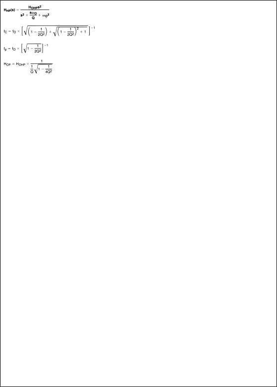
HOHP: the gain (in V/V) of the highpass output as f → fCLK/2 (Figure 3).
www.national.com |
6 |
1.0 Definition of Terms (Continued)
HON: the gain (in V/V) of the notch output as f → 0 Hz and as
f → fCLK/2, when the notch filter has equal gain above and below the center frequency (Figure 4). When the
low-frequency gain differs from the high-frequency gain, as in modes 2 and 3a (Figure 11 and Figure 8), the two quantities below are used in place of HON.
HON1: the gain (in V/V) of the notch output as f → 0 Hz. HON2: the gain (in V/V) of the notch output as f → fCLK/2.
DS010399-5 |
DS010399-6 |
(a) |
(b) |
DS010399-56
FIGURE 1. 2nd-Order Bandpass Response
|
DS010399-7 |
|
DS010399-8 |
(a) |
(b) |
|
DS010399-57
FIGURE 2. 2nd-Order Low-Pass Response
DS010399-9 |
DS010399-10 |
(a) |
(b) |
DS010399-58
FIGURE 3. 2nd-Order High-Pass Response
7 |
www.national.com |
 Loading...