


NNCD10D
NEC NNCD10D, NNCD12D, NNCD3.9D, NNCD5.6D, NNCD4.3D Datasheet
...
©
1996
DATA SHEET
E.S.D NOISE CLIPPING DIODES
NNCD3.3D to NNCD12D
ELECTROSTATIC DISCHARGE NOISE CLIPPING DIODES
(200 mW TYPE)
This product series is a diode developed for E.S.D (Electrostatic
Discharge) noise protection. Based on the IEC1000-4-2 test on
electromagnetic interference (EMI), the diode assures an endur-
ance of no less than 30 kV, thus making itself most suitable for
external interface circuit protection.
Type NNCD3.3D to NNCD12D Series are into 2PIN Super Mini
Mold Package having allowable power dissipation of 200 mW.
FEATURES
• Based on the electrostatic discharge immunity test (IEC1000-4-
2), the product assures the minimum endurance of 30 kV.
• Based on the reference supply of the set, the product achieves
a series over a wide range (15 product name lined up).
APPLICATIONS
• External interface circuit E.S.D protection.
• Circuits for Waveform clipper, Surge absorber.
Document No. D11772EJ2V0DS00 (2nd edition)
Date Published December 1996 N
Printed in Japan
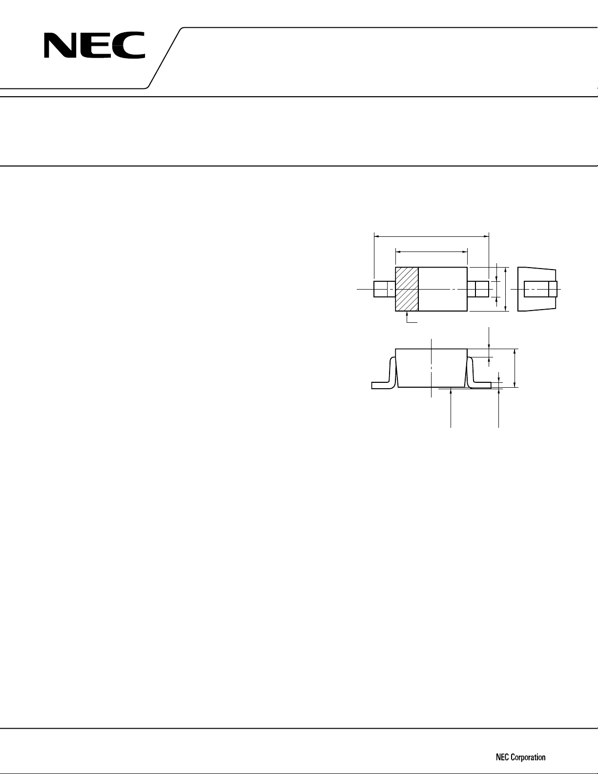
PACKAGE DIMENSIONS
(in millimeters)
MAXIMUM RATINGS (TA = 25 °C)
Power Dissipation P 200 mW
Surge Reverse Power P
RSM 85 W (tT = 10
µ
s 1 pulse) Fig. 6
Junction Temperature Tj 150 °C
Storage Temperature Tstg –55 °C to +150 °C
1.7 ± 0.1
2.5 ± 0.15
0.3 ± 0.05
0 ± 0.05
0.9 ± 0.1
0.19
1.25 ± 0.1
Cathode
Indication
0.11
+0.05
–0.01

NNCD3.3D to NNCD12D
2
ELECTRICAL CHARACTERISTICS (TA = 25 ˚C)
Type Number
Breakdown Voltage
Note 1
Dynamic
Reverse Leakage Capacitance E.S.D Voltage
VBR (V)
Impedance
Note 2
IR (
µ
A) Ct (pF) (kV)
Zz (Ω)
MIN. MAX. IT (mA) MAX. IT (mA) MAX. VR (V) TYP.
TEST
MIN.
TEST
CONDITION CONDITION
NNCD3.3D 3.10 3.50 5 130 5 20 1.0 220 30
NNCD3.6D 3.40 3.80 5 130 5 10 1.0 210 30
NNCD3.9D 3.70 4.10 5 130 5 10 1.0 200 30
NNCD4.3D 4.00 4.49 5 130 5 10 1.0 180 30
NNCD4.7D 4.40 4.92 5 130 5 10 1.0 170 30
NNCD5.1D 4.82 5.39 5 130 5 5 1.5 160 30
C = 150 pF
NNCD5.6D 5.29 5.94 5 80 5 5 2.5 140
VR = 0 V
30
R = 330 Ω
NNCD6.2D 5.84 6.55 5 50 5 5 3.0 120
f = 1 MHz
30
(IEC1000
NNCD6.8D 6.44 7.17 5 30 5 2 3.5 110 30
-4-2)
NNCD7.5D 7.03 7.87 5 30 5 2 4.0 90 30
NNCD8.2D 7.73 8.67 5 30 5 2 5.0 90 30
NNCD9.1D 8.53 9.58 5 30 5 2 6.0 90 30
NNCD10D 9.42 10.58 5 30 5 2 7.0 80 30
NNCD11D 10.40 11.60 5 30 5 2 8.0 70 30
NNCD12D 11.38 12.64 5 35 5 2 9.0 70 30
Notes 1. Tested with pulse (40 ms)
2. Zz is measured at IT give a small A.C. signal.
NNCD3.3D to NNCD12D
3
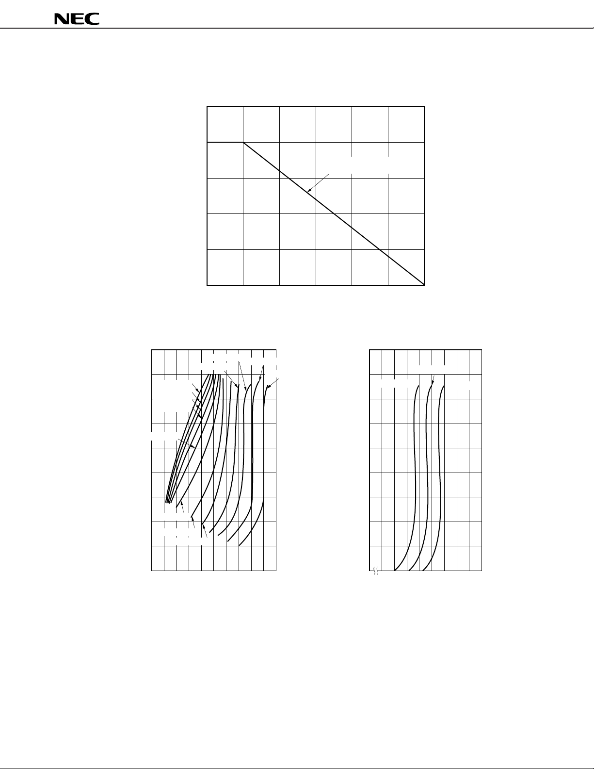
TYPICAL CHARACTERISTICS (TA = 25 °C)
250
200
150
100
50
0
P - Power Dissipation - mW
0 255075
Fig. 1 POWER DISSIPATION vs. AMBIENT TEMPERATURE
100 125 150
T
A
- Ambient Temperature - °C
30 × 30 × 1.6
P.C.B. (Glass Epoxy)
100 m
10 m
1 m
100
10
1
100 n
10 n
1 n
µ
µ
µ
µ
µ
µ
012345678910
V
BR
- Breakdown Voltage - V
I
T
- On State Current - A
100 m
10 m
1 m
100
10
1
100 n
10 n
1 n
0789101112131415
V
BR
- Breakdown Voltage - V
I
T
- On State Current - A
NNCD9.1D
NNCD8.2D
NNCD7.5D
NNCD6.8D
NNCD3.3D
NNCD3.6D
NNCD3.9D
NNCD4.3D
NNCD4.7D
NNCD5.1D
NNCD5.6D
NNCD6.2D
NNCD12D
NNCD10D
NNCD11D
Fig. 2 I
T
- V
BR
CHARACTERISTICS Fig. 3 I
T
- V
BR
CHARACTERISTICS
 Loading...