


 Loading...
NEC PD78F0400, PD78F0410, PD78F0401, PD78F0411, PD78F0402 User Manual
...User’s Manual
78K0/LC3
8-Bit Single-Chip Microcontrollers
μPD78F0400 μPD78F0410 μPD78F0401 μPD78F0411 μPD78F0402 μPD78F0412 μPD78F0403 μPD78F0413
The 78K0/LC3 has an on-chip debug function.
Do not use this product for mass production because its reliability cannot be guaranteed after the on-chip debug function has been used, due to issues with respect to the number of times the flash memory can be rewritten. NEC Electronics does not accept complaints concerning this product.
Document No. U18698EJ1V0UD00 (1st edition)
Date Published June 2007 NS
2007
Printed in Japan
[MEMO]
2
User’s Manual U18698EJ1V0UD

NOTES FOR CMOS DEVICES
1VOLTAGE APPLICATION WAVEFORM AT INPUT PIN
Waveform distortion due to input noise or a reflected wave may cause malfunction. If the input of the CMOS device stays in the area between VIL (MAX) and VIH (MIN) due to noise, etc., the device may malfunction. Take care to prevent chattering noise from entering the device when the input level is fixed, and also in the transition period when the input level passes through the area between VIL (MAX) and VIH (MIN).
2HANDLING OF UNUSED INPUT PINS
Unconnected CMOS device inputs can be cause of malfunction. If an input pin is unconnected, it is possible that an internal input level may be generated due to noise, etc., causing malfunction. CMOS devices behave differently than Bipolar or NMOS devices. Input levels of CMOS devices must be fixed high or low by using pull-up or pull-down circuitry. Each unused pin should be connected to VDD or GND via a resistor if there is a possibility that it will be an output pin. All handling related to unused pins must be judged separately for each device and according to related specifications governing the device.
3PRECAUTION AGAINST ESD
A strong electric field, when exposed to a MOS device, can cause destruction of the gate oxide and ultimately degrade the device operation. Steps must be taken to stop generation of static electricity as much as possible, and quickly dissipate it when it has occurred. Environmental control must be adequate. When it is dry, a humidifier should be used. It is recommended to avoid using insulators that easily build up static electricity. Semiconductor devices must be stored and transported in an anti-static container, static shielding bag or conductive material. All test and measurement tools including work benches and floors should be grounded. The operator should be grounded using a wrist strap. Semiconductor devices must not be touched with bare hands. Similar precautions need to be taken for PW boards with mounted semiconductor devices.
4STATUS BEFORE INITIALIZATION
Power-on does not necessarily define the initial status of a MOS device. Immediately after the power source is turned ON, devices with reset functions have not yet been initialized. Hence, power-on does not guarantee output pin levels, I/O settings or contents of registers. A device is not initialized until the reset signal is received. A reset operation must be executed immediately after power-on for devices with reset functions.
5POWER ON/OFF SEQUENCE
In the case of a device that uses different power supplies for the internal operation and external interface, as a rule, switch on the external power supply after switching on the internal power supply. When switching the power supply off, as a rule, switch off the external power supply and then the internal power supply. Use of the reverse power on/off sequences may result in the application of an overvoltage to the internal elements of the device, causing malfunction and degradation of internal elements due to the passage of an abnormal current.
The correct power on/off sequence must be judged separately for each device and according to related specifications governing the device.
6INPUT OF SIGNAL DURING POWER OFF STATE
Do not input signals or an I/O pull-up power supply while the device is not powered. The current injection that results from input of such a signal or I/O pull-up power supply may cause malfunction and the abnormal current that passes in the device at this time may cause degradation of internal elements. Input of signals during the power off state must be judged separately for each device and according to related specifications governing the device.
User’s Manual U18698EJ1V0UD |
3 |

EEPROM is a trademark of NEC Electronics Corporation.
SuperFlash is a registered trademark of Silicon Storage Technology, Inc. in several countries including the United States and Japan.
Caution: This product uses SuperFlash® technology licensed from Silicon Storage Technology, Inc.
•The information in this document is current as of June, 2007. The information is subject to change without notice. For actual design-in, refer to the latest publications of NEC Electronics data sheets or data books, etc., for the most up-to-date specifications of NEC Electronics products. Not all products and/or types are available in every country. Please check with an NEC Electronics sales representative for availability and additional information.
•No part of this document may be copied or reproduced in any form or by any means without the prior written consent of NEC Electronics. NEC Electronics assumes no responsibility for any errors that may appear in this document.
•NEC Electronics does not assume any liability for infringement of patents, copyrights or other intellectual property rights of third parties by or arising from the use of NEC Electronics products listed in this document or any other liability arising from the use of such products. No license, express, implied or otherwise, is granted under any patents, copyrights or other intellectual property rights of NEC Electronics or others.
•Descriptions of circuits, software and other related information in this document are provided for illustrative purposes in semiconductor product operation and application examples. The incorporation of these circuits, software and information in the design of a customer's equipment shall be done under the full responsibility of the customer. NEC Electronics assumes no responsibility for any losses incurred by customers or third parties arising from the use of these circuits, software and information.
•While NEC Electronics endeavors to enhance the quality, reliability and safety of NEC Electronics products, customers agree and acknowledge that the possibility of defects thereof cannot be eliminated entirely. To minimize risks of damage to property or injury (including death) to persons arising from defects in NEC Electronics products, customers must incorporate sufficient safety measures in their design, such as redundancy, fire-containment and anti-failure features.
•NEC Electronics products are classified into the following three quality grades: "Standard", "Special" and "Specific".
The "Specific" quality grade applies only to NEC Electronics products developed based on a customerdesignated "quality assurance program" for a specific application. The recommended applications of an NEC Electronics product depend on its quality grade, as indicated below. Customers must check the quality grade of each NEC Electronics product before using it in a particular application.
"Standard": Computers, office equipment, communications equipment, test and measurement equipment, audio and visual equipment, home electronic appliances, machine tools, personal electronic equipment and industrial robots.
"Special": Transportation equipment (automobiles, trains, ships, etc.), traffic control systems, anti-disaster systems, anti-crime systems, safety equipment and medical equipment (not specifically designed for life support).
"Specific": Aircraft, aerospace equipment, submersible repeaters, nuclear reactor control systems, life support systems and medical equipment for life support, etc.
The quality grade of NEC Electronics products is "Standard" unless otherwise expressly specified in NEC Electronics data sheets or data books, etc. If customers wish to use NEC Electronics products in applications not intended by NEC Electronics, they must contact an NEC Electronics sales representative in advance to determine NEC Electronics' willingness to support a given application.
(Note)
(1)"NEC Electronics" as used in this statement means NEC Electronics Corporation and also includes its majority-owned subsidiaries.
(2)"NEC Electronics products" means any product developed or manufactured by or for NEC Electronics (as defined above).
M8E 02. 11-1
4 |
User’s Manual U18698EJ1V0UD |

|
|
INTRODUCTION |
|
|
|
|
Readers |
This manual is intended for user engineers who wish to understand the functions of the |
|||||
|
78K0/LC3 and design and develop application systems and programs for these devices. |
|||||
|
The target products are as follows. |
|
|
|
|
|
|
78K0/LC3: μPD78F0400, 78F0401, 78F0402, 78F0403 |
|||||
|
|
μPD78F0410, 78F0411, 78F0412, 78F0413 |
||||
Purpose |
This manual is intended to give users an understanding of the functions described in the |
|||||
|
Organization below. |
|
|
|
|
|
Organization |
The 78K0/LC3 manual is separated into two parts: this manual and the instructions |
|||||
|
edition (common to the 78K0 microcontrollers). |
|
|
|||
|
|
|
|
|
78K/0 Series |
|
|
|
78K0/LC3 |
|
|
|
|
|
|
User’s Manual |
|
|
User’s Manual |
|
|
|
(This Manual) |
|
|
Instructions |
|
|
|
|
|
|
|
|
|
|
|
|
• |
|
|
|
• |
Pin functions |
|
CPU functions |
||
|
• |
Internal block functions |
|
• |
Instruction set |
|
|
• |
Interrupts |
|
• |
Explanation of each instruction |
|
|
• |
Other on-chip peripheral functions |
|
|
|
|
|
• |
Electrical specifications |
|
|
|
|
How to Read This Manual It is assumed that the readers of this manual have general knowledge of electrical engineering, logic circuits, and microcontrollers.
•To gain a general understanding of functions:
→Read this manual in the order of the CONTENTS.
•How to interpret the register format:
→For a bit number enclosed in angle brackets, the bit name is defined as a reserved word in the RA78K0, and is defined as an sfr variable using the #pragma sfr directive in the CC78K0.
•To know details of the 78K0 microcontroller instructions:
→Refer to the separate document 78K/0 Series Instructions User’s Manual (U12326E).
Conventions |
Data significance: |
Higher digits on the left and lower digits on the right |
|
|
Active low representations: |
××× (overscore over pin and signal name) |
|
|
Note: |
Footnote for item marked with Note in the text |
|
|
Caution: |
Information requiring particular attention |
|
|
Remark: |
Supplementary information |
|
|
Numerical representations: |
Binary |
... ×××× or ××××B |
|
|
Decimal |
... ×××× |
|
|
Hexadecimal |
... ××××H |
|
User’s Manual U18698EJ1V0UD |
5 |
|
Related Documents |
The related documents indicated in this publication may include preliminary versions. |
|
|
However, preliminary versions are not marked as such. |
|
Documents Related to Devices |
|
|
|
|
|
|
Document Name |
Document No. |
|
|
|
78K0/LC3 User’s Manual |
|
This manual |
|
|
|
78K/0 Series Instructions User’s Manual |
U12326E |
|
|
|
|
Documents Related to Flash Memory Programming |
|
|
|
|
|
|
Document Name |
Document No. |
|
|
|
PG-FP4 Flash Memory Programmer User’s Manual |
U15260E |
|
|
|
|
PG-FPL3 Flash Memory Programmer User’s Manual |
U17454E |
|
|
|
|
Other Documents |
|
|
|
|
|
|
Document Name |
Document No. |
|
|
|
SEMICONDUCTOR SELECTION GUIDE − Products and Packages − |
X13769X |
|
|
|
|
Semiconductor Device Mount Manual |
Note |
|
Quality Grades on NEC Semiconductor Devices |
C11531E |
|
NEC Semiconductor Device Reliability/Quality Control System |
C10983E |
|
|
|
|
Guide to Prevent Damage for Semiconductor Devices by Electrostatic Discharge (ESD) |
C11892E |
|
|
|
|
Note See the “Semiconductor Device Mount Manual” website (http://www.necel.com/pkg/en/mount/index.html).
Caution The related documents listed above are subject to change without notice. Be sure to use the latest version of each document when designing.
6 |
User’s Manual U18698EJ1V0UD |
CONTENTS
CHAPTER 1 OUTLINE ............................................................................................................................ |
14 |
||||
1.1 |
Features ........................................................................................................................................ |
14 |
|||
1.2 |
Applications.................................................................................................................................. |
15 |
|||
1.3 |
Ordering Information ................................................................................................................... |
15 |
|||
1.4 |
Pin Configuration (Top View)...................................................................................................... |
16 |
|||
1.5 |
78K0/Lx3 Microcontroller Series Lineup ................................................................................... |
19 |
|||
1.6 |
Block Diagram .............................................................................................................................. |
23 |
|||
1.7 |
Outline of Functions .................................................................................................................... |
24 |
|||
CHAPTER 2 PIN FUNCTIONS............................................................................................................... |
27 |
||||
2.1 |
Pin Function List .......................................................................................................................... |
27 |
|||
2.2 |
Description of Pin Functions ...................................................................................................... |
31 |
|||
|
2.2.1 |
P12, P13 (port 1) ............................................................................................................................. |
31 |
||
|
2.2.2 |
P20 to P25 (port 2)........................................................................................................................... |
31 |
||
|
2.2.3 |
P31 to P34 (port 3)........................................................................................................................... |
32 |
||
|
2.2.4 |
P40 (port 4)...................................................................................................................................... |
33 |
||
|
2.2.5 |
P100, P101 (port 10)........................................................................................................................ |
33 |
||
|
2.2.6 |
P112, P113 (port 11)........................................................................................................................ |
33 |
||
|
2.2.7 |
P120 to P124 (port 12)..................................................................................................................... |
34 |
||
|
2.2.8 |
P140 to P143 (port 14)..................................................................................................................... |
34 |
||
|
2.2.9 |
P150 to P153 (port 15)..................................................................................................................... |
35 |
||
|
2.2.10 AVREF (μPD78F041x only) ............................................................................................................ |
35 |
|||
|
2.2.11 AVSS (μPD78F041x only) ............................................................................................................... |
35 |
|||
|
2.2.12 COM0 to COM7 ............................................................................................................................. |
35 |
|||
|
2.2.13 |
|
VLC0 to VLC3 .................................................................................................................................... |
35 |
|
|
|
|
|||
|
2.2.14 |
RESET |
........................................................................................................................................... |
35 |
|
|
2.2.15 REGC ............................................................................................................................................ |
36 |
|||
|
2.2.16 |
|
VDD ................................................................................................................................................. |
36 |
|
|
2.2.17 |
|
VSS ................................................................................................................................................. |
36 |
|
|
2.2.18 FLMD0 ........................................................................................................................................... |
36 |
|||
2.3 |
Pin I/O Circuits and Recommended Connection of Unused Pins........................................... |
37 |
|||
CHAPTER 3 CPU ARCHITECTURE...................................................................................................... |
41 |
||||
3.1 |
Memory Space.............................................................................................................................. |
41 |
|||
|
3.1.1 |
Internal program memory space ...................................................................................................... |
47 |
||
|
3.1.2 |
Internal data memory space ............................................................................................................ |
49 |
||
|
3.1.3 |
Special function register (SFR) area ................................................................................................ |
49 |
||
|
3.1.4 Data memory addressing................................................................................................................. |
50 |
|||
3.2 |
Processor Registers .................................................................................................................... |
54 |
|||
|
3.2.1 |
Control registers............................................................................................................................... |
54 |
||
|
3.2.2 |
General-purpose registers ............................................................................................................... |
58 |
||
|
3.2.3 |
Special function registers (SFRs)..................................................................................................... |
59 |
||
3.3 |
Instruction Address Addressing ................................................................................................ |
64 |
|||
|
|
|
|
User’s Manual U18698EJ1V0UD |
7 |
|
3.3.1 |
Relative addressing......................................................................................................................... |
64 |
|
3.3.2 |
Immediate addressing..................................................................................................................... |
65 |
|
3.3.3 |
Table indirect addressing ................................................................................................................ |
66 |
|
3.3.4 |
Register addressing ........................................................................................................................ |
66 |
3.4 |
Operand Address Addressing .................................................................................................... |
67 |
|
|
3.4.1 |
Implied addressing .......................................................................................................................... |
67 |
|
3.4.2 |
Register addressing ........................................................................................................................ |
68 |
|
3.4.3 |
Direct addressing ............................................................................................................................ |
69 |
|
3.4.4 |
Short direct addressing ................................................................................................................... |
70 |
|
3.4.5 |
Special function register (SFR) addressing..................................................................................... |
71 |
|
3.4.6 |
Register indirect addressing............................................................................................................ |
72 |
|
3.4.7 |
Based addressing ........................................................................................................................... |
73 |
|
3.4.8 |
Based indexed addressing.............................................................................................................. |
74 |
|
3.4.9 |
Stack addressing............................................................................................................................. |
75 |
CHAPTER 4 PORT FUNCTIONS ........................................................................................................... |
76 |
||
4.1 |
Port Functions .............................................................................................................................. |
76 |
|
4.2 |
Port Configuration........................................................................................................................ |
78 |
|
|
4.2.1 |
Port 1 .............................................................................................................................................. |
79 |
|
4.2.2 |
Port 2 .............................................................................................................................................. |
81 |
|
4.2.3 |
Port 3 .............................................................................................................................................. |
83 |
|
4.2.4 |
Port 4 .............................................................................................................................................. |
85 |
|
4.2.5 |
Port 10 ............................................................................................................................................ |
86 |
|
4.2.6 |
Port 11 ............................................................................................................................................ |
87 |
|
4.2.7 |
Port 12 ............................................................................................................................................ |
89 |
|
4.2.8 |
Port 14 ............................................................................................................................................ |
93 |
|
4.2.9 |
Port 15 ............................................................................................................................................ |
94 |
4.3 |
Registers Controlling Port Function .......................................................................................... |
95 |
|
4.4 |
Port Function Operations .......................................................................................................... |
102 |
|
|
4.4.1 |
Writing to I/O port ........................................................................................................................... |
102 |
|
4.4.2 |
Reading from I/O port..................................................................................................................... |
102 |
|
4.4.3 |
Operations on I/O port.................................................................................................................... |
102 |
4.5 |
Settings of PFALL, PF2, PF1, ISC, Port Mode Register, and Output Latch When Using |
|
|
|
Alternate Function...................................................................................................................... |
103 |
|
CHAPTER 5 CLOCK GENERATOR .................................................................................................... |
106 |
||
5.1 |
Functions of Clock Generator................................................................................................... |
106 |
|
5.2 |
Configuration of Clock Generator ............................................................................................ |
107 |
|
5.3 |
Registers Controlling Clock Generator.................................................................................... |
109 |
|
5.4 |
System Clock Oscillator ............................................................................................................ |
120 |
|
|
5.4.1 |
X1 oscillator.................................................................................................................................... |
120 |
|
5.4.2 |
XT1 oscillator ................................................................................................................................. |
120 |
|
5.4.3 When subsystem clock is not used ................................................................................................ |
123 |
|
|
5.4.4 |
Internal high-speed oscillator ......................................................................................................... |
123 |
|
5.4.5 |
Internal low-speed oscillator........................................................................................................... |
123 |
|
5.4.6 |
Prescaler........................................................................................................................................ |
123 |
5.5 |
Clock Generator Operation ....................................................................................................... |
124 |
|
5.6 |
Controlling Clock........................................................................................................................ |
127 |
|
8 |
|
User’s Manual U18698EJ1V0UD |
|
|
5.6.1 |
Example of controlling high-speed system clock ........................................................................... |
127 |
|
5.6.2 |
Example of controlling internal high-speed oscillation clock .......................................................... |
129 |
|
5.6.3 |
Example of controlling subsystem clock ........................................................................................ |
131 |
|
5.6.4 |
Example of controlling internal low-speed oscillation clock............................................................ |
133 |
|
5.6.5 |
Clocks supplied to CPU and peripheral hardware ......................................................................... |
133 |
|
5.6.6 |
CPU clock status transition diagram .............................................................................................. |
134 |
|
5.6.7 |
Condition before changing CPU clock and processing after changing CPU clock......................... |
139 |
|
5.6.8 |
Time required for switchover of CPU clock and main system clock............................................... |
140 |
|
5.6.9 |
Conditions before clock oscillation is stopped................................................................................ |
141 |
|
5.6.10 |
Peripheral hardware and source clocks ....................................................................................... |
142 |
CHAPTER 6 16-BIT TIMER/EVENT COUNTER 00........................................................................... |
143 |
||
6.1 |
Functions of 16-Bit Timer/Event Counter 00 ........................................................................... |
143 |
|
6.2 |
Configuration of 16-Bit Timer/Event Counter 00..................................................................... |
144 |
|
6.3 |
Registers Controlling 16-Bit Timer/Event Counter 00............................................................ |
149 |
|
6.4 |
Operation of 16-Bit Timer/Event Counter 00 ........................................................................... |
158 |
|
|
6.4.1 |
Interval timer operation .................................................................................................................. |
158 |
|
6.4.2 |
Square wave output operation ....................................................................................................... |
161 |
|
6.4.3 |
External event counter operation ................................................................................................... |
164 |
|
6.4.4 |
Operation in clear & start mode entered by TI000 pin valid edge input.......................................... |
168 |
|
6.4.5 |
Free-running timer operation ......................................................................................................... |
181 |
|
6.4.6 |
PPG output operation .................................................................................................................... |
190 |
|
6.4.7 |
One-shot pulse output operation.................................................................................................... |
193 |
|
6.4.8 |
Pulse width measurement operation.............................................................................................. |
198 |
|
6.4.9 |
External 24-bit event counter operation ......................................................................................... |
206 |
|
6.4.10 |
Cautions for external 24-bit event counter ................................................................................... |
210 |
6.5 |
Special Use of TM00 .................................................................................................................. |
212 |
|
|
6.5.1 |
Rewriting CR010 during TM00 operation....................................................................................... |
212 |
|
6.5.2 Setting LVS00 and LVR00 ............................................................................................................. |
212 |
|
6.6 |
Cautions for 16-Bit Timer/Event Counter 00 ........................................................................... |
214 |
|
CHAPTER 7 8-BIT TIMER/EVENT COUNTERS 50, 51, AND 52 .................................................. |
218 |
||
7.1 |
Functions of 8-Bit Timer/Event Counters 50, 51, and 52 ....................................................... |
218 |
|
7.2 |
Configuration of 8-Bit Timer/Event Counters 50, 51, and 52 ................................................. |
218 |
|
7.3 |
Registers Controlling 8-Bit Timer/Event Counters 50, 51, and 52 ........................................ |
222 |
|
7.4 |
Operations of 8-Bit Timer/Event Counters 50, 51, and 52...................................................... |
229 |
|
|
7.4.1 |
Operation as interval timer............................................................................................................. |
229 |
|
7.4.2 |
Operation as external event counter (TM52 only).......................................................................... |
231 |
7.5 |
Cautions for 8-Bit Timer/Event Counters 50, 51, and 52........................................................ |
232 |
|
CHAPTER 8 8-BIT TIMERS H0, H1 AND H2................................................................................... |
234 |
||
8.1 |
Functions of 8-Bit Timers H0, H1, and H2 ............................................................................... |
234 |
|
8.2 |
Configuration of 8-Bit Timers H0, H1, and H2......................................................................... |
234 |
|
8.3 |
Registers Controlling 8-Bit Timers H0, H1, and H2 ................................................................ |
239 |
|
8.4 |
Operation of 8-Bit Timers H0, H1 and H2................................................................................. |
246 |
|
|
8.4.1 |
Operation as interval timer/square-wave output ............................................................................ |
246 |
|
8.4.2 Operation as PWM output.............................................................................................................. |
249 |
|
|
|
User’s Manual U18698EJ1V0UD |
9 |
|
8.4.3 |
Carrier generator operation (8-bit timer H1 only)............................................................................ |
255 |
CHAPTER 9 REAL-TIME COUNTER................................................................................................... |
262 |
||
9.1 Functions of Real-Time Counter............................................................................................... |
262 |
||
9.2 Configuration of Real-Time Counter ........................................................................................ |
262 |
||
9.3 Registers Controlling Real-Time Counter................................................................................ |
264 |
||
9.4 Real-Time Counter Operation ................................................................................................... |
276 |
||
|
9.4.1 |
Starting operation of real-time counter ........................................................................................... |
276 |
|
9.4.2 |
Reading/writing real-time counter................................................................................................... |
277 |
|
9.4.3 |
Setting alarm of real-time counter .................................................................................................. |
279 |
CHAPTER 10 |
WATCHDOG TIMER ..................................................................................................... |
280 |
|
10.1 |
Functions of Watchdog Timer................................................................................................. |
280 |
|
10.2 |
Configuration of Watchdog Timer .......................................................................................... |
281 |
|
10.3 |
Register Controlling Watchdog Timer.................................................................................... |
282 |
|
10.4 |
Operation of Watchdog Timer................................................................................................. |
283 |
|
|
10.4.1 |
Controlling operation of watchdog timer....................................................................................... |
283 |
|
10.4.2 |
Setting overflow time of watchdog timer....................................................................................... |
284 |
|
10.4.3 |
Setting window open period of watchdog timer............................................................................ |
285 |
CHAPTER 11 |
BUZZER OUTPUT CONTROLLER.............................................................................. |
287 |
|
11.1 |
Functions of Buzzer Output Controller.................................................................................. |
287 |
|
11.2 |
Configuration of Buzzer Output Controller ........................................................................... |
288 |
|
11.3 |
Registers Controlling Buzzer Output Controller................................................................... |
288 |
|
11.4 |
Operations of Buzzer Output Controller ................................................................................ |
290 |
|
CHAPTER 12 |
10-BIT SUCCESSIVE APPROXIMATION TYPE A/D CONVERTER |
|
|
|
|
(μPD78F041x only) ........................................................................................................ |
291 |
12.1 |
Function of 10-Bit Successive Approximation Type A/D Converter................................... |
291 |
|
12.2 |
Configuration of 10-Bit Successive Approximation Type A/D Converter .......................... |
292 |
|
12.3 |
Registers Used in 10-Bit Successive Approximation Type A/D Converter........................ |
294 |
|
12.4 |
10-Bit Successive Approximation Type A/D Converter Operations ................................... |
302 |
|
|
12.4.1 |
Basic operations of A/D converter................................................................................................ |
302 |
|
12.4.2 |
Input voltage and conversion results............................................................................................ |
304 |
|
12.4.3 |
A/D converter operation mode ..................................................................................................... |
305 |
12.5 |
How to Read A/D Converter Characteristics Table............................................................... |
307 |
|
12.6 |
Cautions for 10-Bit Successive Approximation Type A/D Converter ................................. |
309 |
|
CHAPTER 13 |
SERIAL INTERFACE UART0 ...................................................................................... |
313 |
|
13.1 |
Functions of Serial Interface UART0...................................................................................... |
313 |
|
13.2 |
Configuration of Serial Interface UART0 ............................................................................... |
314 |
|
13.3 |
Registers Controlling Serial Interface UART0....................................................................... |
317 |
|
13.4 |
Operation of Serial Interface UART0 ...................................................................................... |
323 |
|
|
13.4.1 Operation stop mode.................................................................................................................... |
323 |
|
|
13.4.2 |
Asynchronous serial interface (UART) mode ............................................................................... |
324 |
|
13.4.3 |
Dedicated baud rate generator..................................................................................................... |
330 |
10 |
|
User’s Manual U18698EJ1V0UD |
|
|
13.4.4 |
Calculation of baud rate ............................................................................................................... |
331 |
CHAPTER 14 |
SERIAL INTERFACE UART6...................................................................................... |
335 |
|
14.1 |
Functions of Serial Interface UART6...................................................................................... |
335 |
|
14.2 |
Configuration of Serial Interface UART6 ............................................................................... |
339 |
|
14.3 |
Registers Controlling Serial Interface UART6....................................................................... |
342 |
|
14.4 |
Operation of Serial Interface UART6...................................................................................... |
353 |
|
|
14.4.1 Operation stop mode ................................................................................................................... |
353 |
|
|
14.4.2 |
Asynchronous serial interface (UART) mode............................................................................... |
354 |
|
14.4.3 |
Dedicated baud rate generator .................................................................................................... |
368 |
|
14.4.4 |
Calculation of baud rate ............................................................................................................... |
370 |
CHAPTER 15 |
LCD CONTROLLER/DRIVER....................................................................................... |
376 |
|
15.1 |
Functions of LCD Controller/Driver ....................................................................................... |
376 |
|
15.2 |
Configuration of LCD Controller/Driver ................................................................................. |
378 |
|
15.3 |
Registers Controlling LCD Controller/Driver ........................................................................ |
380 |
|
15.4 |
Setting LCD Controller/Driver................................................................................................. |
385 |
|
15.5 |
LCD Display Data Memory ...................................................................................................... |
386 |
|
15.6 |
Common and Segment Signals .............................................................................................. |
387 |
|
15.7 |
Display Modes .......................................................................................................................... |
393 |
|
|
15.7.1 |
Static display example ................................................................................................................. |
393 |
|
15.7.2 |
Two-time-slice display example ................................................................................................... |
396 |
|
15.7.3 |
Three-time-slice display example................................................................................................. |
399 |
|
15.7.4 |
Four-time-slice display example .................................................................................................. |
403 |
15.8 |
Supplying LCD Drive Voltages VLC0, VLC1, VLC2 and VLC3 ..................................................... |
406 |
|
|
15.8.1 |
Internal resistance division method.............................................................................................. |
406 |
|
15.8.2 |
External resistance division method............................................................................................. |
408 |
CHAPTER 16 |
MANCHESTER CODE GENERATOR......................................................................... |
410 |
|
16.1 |
Functions of Manchester Code Generator ............................................................................ |
410 |
|
16.2 |
Configuration of Manchester Code Generator...................................................................... |
410 |
|
16.3 |
Registers Controlling Manchester Code Generator ............................................................. |
413 |
|
16.4 |
Operation of Manchester Code Generator ............................................................................ |
416 |
|
|
16.4.1 Operation stop mode ................................................................................................................... |
416 |
|
|
16.4.2 Manchester code generator mode ............................................................................................... |
417 |
|
|
16.4.3 |
Bit sequential buffer mode ........................................................................................................... |
426 |
CHAPTER 17 |
INTERRUPT FUNCTIONS ............................................................................................ |
435 |
|
17.1 |
Interrupt Function Types......................................................................................................... |
435 |
|
17.2 |
Interrupt Sources and Configuration ..................................................................................... |
435 |
|
17.3 |
Registers Controlling Interrupt Functions ............................................................................ |
440 |
|
17.4 |
Interrupt Servicing Operations ............................................................................................... |
447 |
|
|
17.4.1 |
Maskable interrupt acknowledgment............................................................................................ |
447 |
|
17.4.2 |
Software interrupt request acknowledgment................................................................................ |
449 |
|
17.4.3 |
Multiple interrupt servicing ........................................................................................................... |
450 |
|
17.4.4 |
Interrupt request hold................................................................................................................... |
453 |
|
|
User’s Manual U18698EJ1V0UD |
11 |
CHAPTER 18 KEY INTERRUPT FUNCTION ..................................................................................... |
454 |
|
18.1 |
Functions of Key Interrupt ...................................................................................................... |
454 |
18.2 |
Configuration of Key Interrupt................................................................................................ |
454 |
18.3 |
Register Controlling Key Interrupt ......................................................................................... |
455 |
CHAPTER 19 STANDBY FUNCTION .................................................................................................. |
456 |
|
19.1 |
Standby Function and Configuration..................................................................................... |
456 |
|
19.1.1 Standby func |
|
12 |
User’s Manual U18698EJ1V0UD |
|
24.5.5 REGC pin..................................................................................................................................... |
515 |
|
|
24.5.6 |
Other signal pins.......................................................................................................................... |
516 |
|
24.5.7 |
Power supply ............................................................................................................................... |
516 |
24.6 |
Programming Method .............................................................................................................. |
517 |
|
|
24.6.1 |
Controlling flash memory ............................................................................................................. |
517 |
|
24.6.2 Flash memory programming mode .............................................................................................. |
517 |
|
|
24.6.3 |
Selecting communication mode ................................................................................................... |
518 |
|
24.6.4 Communication commands ......................................................................................................... |
519 |
|
24.7 |
Security Settings...................................................................................................................... |
520 |
|
24.8 |
Flash Memory Programming by Self-Programming (Under Development) ....................... |
522 |
|
|
24.8.1 |
Boot swap function....................................................................................................................... |
524 |
CHAPTER 25 |
ON-CHIP DEBUG FUNCTION..................................................................................... |
526 |
|
25.1 |
Connecting QB-78K0MINI to 78K0/LC3 .................................................................................. |
526 |
|
25.2 |
On-Chip Debug Security ID ..................................................................................................... |
527 |
|
CHAPTER 26 |
INSTRUCTION SET ...................................................................................................... |
528 |
|
26.1 |
Conventions Used in Operation List...................................................................................... |
528 |
|
|
26.1.1 |
Operand identifiers and specification methods ............................................................................ |
528 |
|
26.1.2 |
Description of operation column .................................................................................................. |
529 |
|
26.1.3 |
Description of flag operation column............................................................................................ |
529 |
26.2 |
Operation List........................................................................................................................... |
530 |
|
26.3 |
Instructions Listed by Addressing Type ............................................................................... |
538 |
|
CHAPTER 27 |
ELECTRICAL SPECIFICATIONS (STANDARD PRODUCTS).................................. |
541 |
|
CHAPTER 28 |
PACKAGE DRAWINGS................................................................................................ |
559 |
|
CHAPTER 29 |
CAUTIONS FOR WAIT ................................................................................................ |
560 |
|
29.1 |
Cautions for Wait ..................................................................................................................... |
560 |
|
29.2 |
Peripheral Hardware That Generates Wait ............................................................................ |
561 |
|
User’s Manual U18698EJ1V0UD |
13 |

CHAPTER 1 OUTLINE
1.1Features
{Minimum instruction execution time can be changed from high speed (0.2 μs: @ 10 MHz operation with highspeed system clock) to ultra low-speed (122 μs: @ 32.768 kHz operation with subsystem clock)
{General-purpose register: 8 bits × 32 registers (8 bits × 8 registers × 4 banks)
{ROM, RAM capacities
Item |
Program Memory |
Data Memory |
||||
|
(ROM) |
|
Internal High-Speed RAM |
Note |
LCD Display RAM |
|
|
|
|
|
|
||
Part Number |
|
|
|
|
|
|
μPD78F0400, 78F0410 |
Flash |
|
8 KB |
512 bytes |
|
22 × 4 bits (with 4 com) |
μPD78F0401, 78F0411 |
memoryNote |
|
16 KB |
768 bytes |
|
18 × 8 bits (with 8 com) |
μPD78F0402, 78F0412 |
|
|
24 KB |
1 KB |
|
|
μPD78F0403, 78F0413 |
|
|
32 KB |
|
|
|
Note The internal flash memory and internal high-speed RAM capacities can be changed using the internal memory size switching register (IMS).
{On-chip single-power-supply flash memory
{Self-programming (with boot swap function)
{On-chip debug function
{On-chip power-on-clear (POC) circuit and low-voltage detector (LVI)
{On-chip watchdog timer (operable with internal low-speed oscillation clock)
{LCD controller/driver (external resistance division and internal resistance division are switchable)
•Segment signals: 22, Common signals: 4 (with 4com)
•Segment signals: 18, Common signals: 8 (with 8com)
{On-chip key interrupt function: 3 channels
{On-chip buzzer output controller
{I/O ports: 30
{Timer: 9 channels
•16-bit timer/event counter: 1 channel
•8-bit timer/event counter: 3 channels
• 8-bit timer: |
3 channels |
|
• |
Real-time counter (RTC): |
1 channel |
• |
Watchdog timer: |
1 channel |
{Serial interface: 2 channels
• UART (LIN (Local Interconnect Network)-bus supported): 1 channel
• UART: |
1 channel |
{10-bit successive approximation type A/D converter: 6 channels (μPD78F041x only)
{Manchester code generator
{Power supply voltage: VDD = 1.8 to 5.5 V
{Operating ambient temperature: TA = −40 to +85°C
14 |
User’s Manual U18698EJ1V0UD |

CHAPTER 1 OUTLINE
1.2 Applications
Digital cameras, AV equipments, household electrical appliances, utility meters, health care equipments, and measurement equipment, etc.
1.3Ordering Information
•Flash memory version (Lead-free products)
Part Number |
Package |
μPD78F0400GA-GAM-AX |
48-pin plastic LQFP (fine pitch) (7 × 7) |
μPD78F0401GA-GAM-AX |
48-pin plastic LQFP (fine pitch) (7 × 7) |
μPD78F0402GA-GAM-AX |
48-pin plastic LQFP (fine pitch) (7 × 7) |
μPD78F0403GA-GAM-AX |
48-pin plastic LQFP (fine pitch) (7 × 7) |
μPD78F0410GA-GAM-AX |
48-pin plastic LQFP (fine pitch) (7 × 7) |
μPD78F0411GA-GAM-AX |
48-pin plastic LQFP (fine pitch) (7 × 7) |
μPD78F0412GA-GAM-AX |
48-pin plastic LQFP (fine pitch) (7 × 7) |
μPD78F0413GA-GAM-AX |
48-pin plastic LQFP (fine pitch) (7 × 7) |
User’s Manual U18698EJ1V0UD |
15 |
CHAPTER 1 OUTLINE
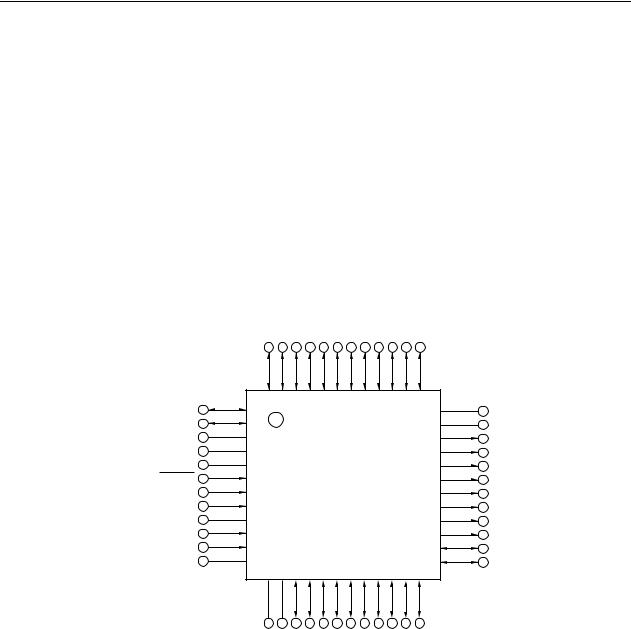
1.4 Pin Configuration (Top View)
(1)μPD78F0400, 78F0401, 78F0402, 78F0403
•48-pin plastic LQFP (fine pitch) (7 × 7)
P12/RxD0/KR3/<RxD6> |
P13/TxD0/KR4/<TxD6> |
P34/TI52/TI010/TO00/RTC1HZ/INTP1 |
P33/TI000/RTCDIV/RTCCL/BUZ/INTP2 |
P32/TOH0/MCGO |
P31/TOH1/INTP3 |
P20/SEG21 |
P21/SEG20 |
P22/SEG19 |
P23/SEG18 |
P24/SEG17 |
P25/SEG16 |
INTP0/EXLVI/P120 |
1 |
48 47 46 45 44 43 42 41 40 39 38 37 |
36 |
||
KR0/VLC3/P40 |
2 |
35 |
VLC2 |
3 |
34 |
VLC1 |
4 |
33 |
VLC0 |
5 |
32 |
RESET |
6 |
31 |
XT2/P124 |
7 |
30 |
XT1/P123 |
8 |
29 |
FLMD0 |
9 |
28 |
OCD0B/EXCLK/X2/P122 |
10 |
27 |
OCD0A/X1/P121 |
11 |
26 |
REGC |
12 |
25 |
|
|
13 14 15 16 17 18 19 20 21 22 23 24 |
VSS
VDD
COM0
COM1
COM2
COM3
COM4/SEG0
COM5/SEG1
COM6/SEG2
COM7/SEG3
P100/SEG4
P101/SEG5
SSDDSEG15/P153SEG14/P152SEG13/P151SEG12/P150SEG11/P143SEG10/P142SEG9/P141SEG8/P140RxD6/SEG7/P113TxD6/SEG6/P112
VV
Cautions 1. Connect the REGC pin to VSS via a capacitor (0.47 to 1 μF: recommended).
2.Only the bottom side pins (pin numbers 23 and 24) correspond to the UART6 pins (RxD6 and TxD6) when writing by a flash memory programmer. Writing cannot be performed by the top side pins (pin numbers 48 and 47).
3.Make VDD (pin number 14) and VDD (pin number 35), VSS (pin number 13) and VSS (pin number 36) the same potential.
Remark The functions within arrowheads (< >) can be assigned by setting the input switch control register (ISC).
16 |
User’s Manual U18698EJ1V0UD |
CHAPTER 1 OUTLINE
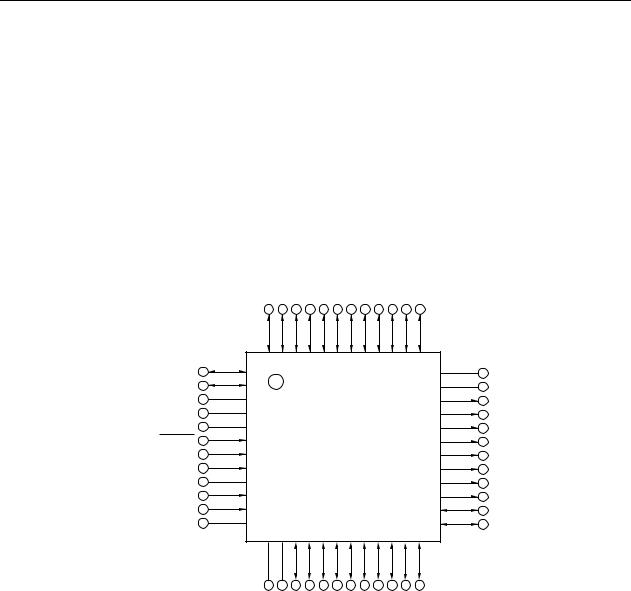
(2)μPD78F0410, 78F0411, 78F0412, 78F0413
•48-pin plastic LQFP (fine pitch) (7 × 7)
P12/RxD0/KR3/<RxD6> |
P13/TxD0/KR4/<TxD6> |
P34/TI52/TI010/TO00/RTC1HZ/INTP1 |
P33/TI000/RTCDIV/RTCCL/BUZ/INTP2 |
P32/TOH0/MCGO |
P31/TOH1/INTP3 |
P20/SEG21/ANI0 |
P21/SEG20/ANI1 |
P22/SEG19/ANI2 |
P23/SEG18/ANI3 |
P24/SEG17/ANI4 |
P25/SEG16/ANI5 |
INTP0/EXLVI/P120 |
1 |
48 47 46 45 44 43 42 41 40 39 38 37 |
36 |
||
KR0/VLC3/P40 |
2 |
35 |
VLC2 |
3 |
34 |
VLC1 |
4 |
33 |
VLC0 |
5 |
32 |
RESET |
6 |
31 |
XT2/P124 |
7 |
30 |
XT1/P123 |
8 |
29 |
FLMD0 |
9 |
28 |
OCD0B/EXCLK/X2/P122 |
10 |
27 |
OCD0A/X1/P121 |
11 |
26 |
REGC |
12 |
25 |
|
|
13 14 15 16 17 18 19 20 21 22 23 24 |
AVSS
AVREF
COM0
COM1
COM2
COM3
COM4/SEG0
COM5/SEG1
COM6/SEG2
COM7/SEG3
P100/SEG4
P101/SEG5
VSS |
VDD |
SEG15/P153 |
SEG14/P152 |
SEG13/P151 |
SEG12/P150 |
SEG11/P143 |
SEG10/P142 |
SEG9/P141 |
SEG8/P140 |
RxD6/SEG7/P113 |
TxD6/SEG6/P112 |
Cautions 1. Connect the AVSS pin to VSS.
2.Connect the REGC pin to VSS via a capacitor (0.47 to 1 μF: recommended).
3.ANI0/P20 to ANI5/P25 are set in the analog input mode after release of reset.
4.Only the bottom side pins (pin numbers 23 and 24) correspond to the UART6 pins (RxD6 and TxD6) when writing by a flash memory programmer. Writing cannot be performed by the top side pins (pin numbers 48 and 47).
Remark The functions within arrowheads (< >) can be assigned by setting the input switch control register (ISC).
User’s Manual U18698EJ1V0UD |
17 |

CHAPTER 1 OUTLINE
Pin Identification |
|
|
|
|
ANI0 to ANI5Note: |
Analog input |
P150 to P153: |
Port 15 |
|
AVREFNote: |
Analog reference voltage |
REGC |
Regulator capacitance |
|
AVSSNote: |
Analog ground |
|
Reset |
|
RESET: |
|
|||
BUZ: |
Buzzer output |
RxD0, RxD6: |
Receive data |
|
COM0 to COM7: |
Common output |
RTC1HZ: |
Real-time counter correction |
|
EXCLK: |
External clock input |
|
|
clock (1 Hz) output |
|
(main system clock) |
RTCCL: |
Real-time counter clock (32.768 |
|
EXLVI: |
External potential input |
|
|
kHz original oscillation) output |
|
for low-voltage detector |
RTCDIV: |
Real-time counter clock (32.768 |
|
FLMD0: |
Flash programming mode |
|
|
kHz divided frequency) output |
INTP0 to INTP3: |
External interrupt input |
SEG0 to SEG21: |
Segment output |
|
KR0, KR3, KR4: |
Key return |
TI000, TI010: |
Timer input |
|
MCGO: |
Manchester code generator output |
TO00: |
Timer output |
|
OCD0A, OCD0B: |
On chip debug input/output |
TOH0, TOH1: |
Timer output |
|
P12, P13: |
Port 1 |
TxD0, TxD6: |
Transmit data |
|
P20 to P25: |
Port 2 |
VDD: |
Power supply |
|
P31 to P34: |
Port 3 |
VSS: |
Ground |
|
P40: |
Port 4 |
VLC0 to VLC3: |
LCD power supply |
|
P100, P101: |
Port 10 |
X1, X2: |
Crystal oscillator |
|
P112, P113: |
Port 11 |
|
|
(main system clock) |
P120 to P124: |
Port 12 |
XT1, XT2: |
Crystal oscillator |
|
P140 to P143: |
Port 14 |
|
|
(subsystem clock) |
Note μPD78F041x only.
18 |
User’s Manual U18698EJ1V0UD |

CHAPTER 1 OUTLINE
1.5 78K0/Lx3 Microcontroller Series Lineup
ROM |
RAM |
78K0/LC3 |
78K0/LD3 |
78K0/LE3 |
78K0/LF3 |
|
|
48 Pins |
52 Pins |
64 Pins |
80 Pins |
|
|
|
|
|
|
60 KB |
2 KB |
− |
− |
μPD78F0465 |
μPD78F0495 |
|
|
|
|
μPD78F0455 |
μPD78F0485 |
|
|
|
|
μPD78F0445 |
μPD78F0475 |
48 KB |
2 KB |
− |
− |
μPD78F0464 |
μPD78F0494 |
|
|
|
|
μPD78F0454 |
μPD78F0484 |
|
|
|
|
μPD78F0444 |
μPD78F0474 |
|
|
|
|
|
|
32 KB |
1 KB |
μPD78F0413 |
μPD78F0433 |
μPD78F0463 |
μPD78F0493 |
|
|
μPD78F0403 |
μPD78F0423 |
μPD78F0453 |
μPD78F0483 |
|
|
|
|
μPD78F0443 |
μPD78F0473 |
|
|
|
|
|
|
24 KB |
1 KB |
μPD78F0412 |
μPD78F0432 |
μPD78F0462 |
μPD78F0492 |
|
|
μPD78F0402 |
μPD78F0422 |
μPD78F0452 |
μPD78F0482 |
|
|
|
|
μPD78F0442 |
μPD78F0472 |
16 KB |
768 B |
μPD78F0411 |
μPD78F0431 |
μPD78F0461 |
μPD78F0491 |
|
|
μPD78F0401 |
μPD78F0421 |
μPD78F0451 |
μPD78F0481 |
|
|
|
|
μPD78F0441 |
μPD78F0471 |
|
|
|
|
|
|
8 KB |
512 B |
μPD78F0410 |
μPD78F0430 |
− |
− |
|
|
μPD78F0400 |
μPD78F0420 |
|
|
|
|
|
|
|
|
User’s Manual U18698EJ1V0UD |
19 |

CHAPTER 1 OUTLINE
The list of functions in the 78K0/Lx3 Microcontrollers is shown below. |
|
|
|
|
|
|
|
(1/3) |
||||||||
Part Number |
|
|
|
78K0/LC3 |
|
|
|
|
|
|
78K0/LD3 |
|
|
|
||
|
|
μPD78F040x |
|
|
μPD78F041x |
|
|
μPD78F042x |
|
|
μPD78F043x |
|
||||
Item |
|
|
|
48 Pins |
|
|
|
|
|
|
52 Pins |
|
|
|
||
Flash memory (KB) |
8 |
16 |
24 |
32 |
8 |
16 |
24 |
32 |
8 |
16 |
24 |
32 |
8 |
16 |
24 |
32 |
RAM (KB) |
0.5 |
0.75 |
1 |
1 |
0.5 |
0.75 |
1 |
1 |
0.5 |
0.75 |
1 |
1 |
0.5 |
0.75 |
1 |
1 |
Power supply voltage |
|
|
|
|
|
|
VDD = 1.8 to 5.5 V |
|
|
|
|
|
|
|||
Regulator |
|
|
|
|
|
|
|
Provided |
|
|
|
|
|
|
|
|
Minimum instruction |
|
|
0.2 μs (10 MHz: VDD = 2.7 to 5.5 V)/ 0.4 μs (5 MHz: VDD = 1.8 to 5.5 V) |
|
|
|||||||||||
execution time |
|
|
|
|
|
|
|
|
|
|
|
|
|
|
|
|
|
|
|
|
High-speed system |
10 MHz: VDD = 2.7 to 5.5 V/5 MHz: VDD = 1.8 to 5.5 V |
|
||||||
|
Main |
|
clock |
|
|
|
|
|
|
|
||
Clock |
|
Internal high-speed |
|
|
8 MHz (TYP.): VDD = 1.8 to 5.5 V |
|
||||||
|
|
|
|
|
|
|
||||||
|
|
|
|
oscillation clock |
|
|
|
|
|
|
|
|
|
Subclock |
|
|
32.768 kHz (TYP.): VDD = 1.8 to 5.5 V |
|
|||||||
|
Internal low-speed |
|
|
240 kHz (TYP.): VDD = 1.8 to 5.5 V |
|
|||||||
|
oscillation clock |
|
|
|
|
|
|
|
||||
Port |
Total |
30 |
|
|
34 |
|
||||||
|
|
|
|
|
|
|
|
|
|
|
|
|
|
|
|
|
|
|
|
|
|
|
|
||
|
16 bits (TM0) |
|
|
|
1 ch |
|
||||||
Timer |
8 bits (TM5) |
|
|
|
3 ch |
|
||||||
8 bits (TMH) |
|
|
|
3 ch |
|
|||||||
|
|
|
|
|
||||||||
|
RTC |
|
|
|
1 ch |
|
||||||
|
WDT |
|
|
|
1 ch |
|
||||||
interface |
3-wire CSI |
− |
|
|
1 chNote 1 |
|
||||||
UART supporting LIN- |
1 chNote 2 |
|
|
1 chNote 3 |
|
|||||||
|
UART |
1 ch |
|
|
1 chNote 1 |
|
||||||
Serial |
bus |
|
|
|
|
|
|
|
|
|
||
|
|
|
|
|
|
|
|
|
|
|
|
|
|
|
|
|
|
|
|
|
|
||||
LCD |
Type |
External resistance division and internal resistance division are switchable. |
|
|||||||||
Segment signal |
22 (18)Note 4 |
|
|
24 (20)Note 4 |
|
|||||||
|
|
|
|
|||||||||
|
Common signal |
|
|
|
4 (8)Note 4 |
|
||||||
10-bit successive |
− |
|
6 ch |
|
− |
|
6 ch |
|||||
approximation type A/D |
|
|
|
|
|
|
|
|||||
16-bit ΔΣ type A/D |
|
|
|
− |
|
|||||||
Interrupt |
External |
|
|
|
5 |
|
|
|||||
|
|
|
|
|
|
|
|
|
|
|
|
|
Internal |
17 |
|
18 |
|
19 |
|
20 |
|||||
|
|
|
|
|||||||||
|
|
|
|
|
|
|
|
|
|
|
||
Key interrupt |
3 ch |
|
|
5 ch |
|
|||||||
|
|
RESET |
pin |
|
|
|
Provided |
|
||||
Reset |
|
|
|
|
|
|||||||
POC |
1.59 V ±0.15 V (Time for rising up to 1.8 V : 3.6 ms (MAX.)) |
|
||||||||||
|
|
|
|
|
|
|
|
|
|
|
|
|
LVI |
|
|
The detection level of the supply voltage is selectable in 16 steps. |
|
||||||||
|
|
|
|
|||||||||
|
WDT |
|
|
|
Provided |
|
||||||
|
|
|
|
|
|
|
|
|
||||
Clock output |
|
|
|
− |
|
|||||||
Buzzer output |
|
|
|
Provided |
|
|||||||
|
|
|
|
|
|
|
|
|||||
Remote controller receiver |
− |
|
|
Provided |
|
|||||||
MCG |
|
|
|
|
|
Provided |
|
|||||
|
|
|
|
|
|
|
|
|||||
On-chip debug function |
|
|
|
Provided |
|
|||||||
Operating ambient temperature |
|
|
|
TA = −40 to +85°C |
|
|||||||
Notes 1. Since 3-wire CSI and UART are used as alternate-function pins, they must be assigned to either of the functions for use.
2.The LIN-bus supporting UART pins can be changed to the UART pins (pin numbers 47 and 48).
3.The LIN-bus supporting UART pins can be changed to the 3-wire CSI/UART pins (pin numbers 50 and 51).
4.The values in parentheses are the number of signal outputs when 8com is used.
20 |
User’s Manual U18698EJ1V0UD |

CHAPTER 1 OUTLINE
Part Number
Item
Flash memory (KB)
RAM (KB)
Power supply voltage
Regulator
Minimum instruction execution time
|
|
High-speed system |
|
|
Main |
clock |
|
Clock |
Internal high-speed |
||
|
|
||
|
|
oscillation clock |
|
|
Subclock |
||
|
Internal low-speed |
||
|
oscillation clock |
||
Port |
Total |
||
|
|
||
|
|
||
|
16 bits (TM0) |
||
Timer |
8 bits (TM5) |
||
8 bits (TMH) |
|||
|
|||
|
RTC |
||
|
WDT |
||
interface |
3-wire CSI/UARTNote1 |
||
|
|
||
UART supporting LIN- |
|||
Serial |
|||
bus Note2 |
|||
|
|||
LCD |
Type |
||
Segment signal |
|||
|
|||
|
Common signal |
||
|
|
|
|
10-bit successive approximation type A/D
16-bit ΔΣ type A/D
Interrupt |
External |
|||
Internal |
||||
|
||||
|
|
|
|
|
Key interrupt |
||||
|
|
|
|
|
|
|
RESET |
pin |
|
Reset |
|
|
|
|
POC |
||||
|
|
|
||
LVI |
||||
|
||||
|
WDT |
|||
|
|
|
|
|
Clock output
Buzzer output
Remote controller receiver
MCG
On-chip debug function
Operating ambient temperature
|
|
|
|
|
|
|
|
|
|
|
|
|
|
|
|
(2/3) |
|
|
|
|
|
|
|
78K0/LE3 |
|
|
|
|
|
|
|
||
|
μPD78F044x |
|
|
μPD78F045x |
|
|
μPD78F046x |
|
||||||||
|
|
|
|
|
|
|
64 Pins |
|
|
|
|
|
|
|
||
16 |
24 |
32 |
48 |
60 |
16 |
24 |
|
32 |
|
48 |
60 |
16 |
24 |
32 |
48 |
60 |
0.75 |
1 |
1 |
2 |
2 |
0.75 |
1 |
|
1 |
|
2 |
2 |
0.75 |
1 |
1 |
2 |
2 |
|
|
|
|
|
|
VDD = 1.8 to 5.5 V |
|
|
|
|
|
|
||||
Provided
0.2 μs (10 MHz: VDD = 2.7 to 5.5 V)/ 0.4 μs (5 MHz: VDD = 1.8 to 5.5 V)
10 MHz: VDD = 2.7 to 5.5 V/5 MHz: VDD = 1.8 to 5.5 V
8 MHz (TYP.): VDD = 1.8 to 5.5 V
32.768 kHz (TYP.): VDD = 1.8 to 5.5 V 240 kHz (TYP.): VDD = 1.8 to 5.5 V
46
1 ch
3 ch
3 ch
1 ch
1 ch
1 ch
1 ch
External resistance division and internal resistance division are switchable.
|
32 (28)Note 3 |
|
24 (20)Note 3 |
|
|
|
4 (8)Note 3 |
|
|
− |
|
|
8 ch |
|
|
|
|
|
|
|
− |
|
3 ch |
|
|
6 |
|
|
|
19 |
|
20 |
|
21 |
|
|
|
|
|
5 ch Provided
1.59 V ±0.15 V (Time for rising up to 1.8 V : 3.6 ms (MAX.)) The detection level of the supply voltage is selectable in 16 steps. Provided
−
Provided
Provided
Provided
Provided
TA = −40 to +85°C
Notes 1. Select either of the functions of these alternate-function pins.
2.The LIN-bus supporting UART pins can be changed to the 3-wire CSI/UART pins (pin numbers 62 and 63).
3.The values in parentheses are the number of signal outputs when 8com is used.
User’s Manual U18698EJ1V0UD |
21 |

CHAPTER 1 OUTLINE
|
|
|
|
|
|
|
|
|
|
|
|
|
|
|
|
|
|
|
|
|
|
|
|
|
|
|
(3/3) |
|
|
|
|
|
Part Number |
|
|
|
|
|
|
|
|
|
|
78K0/LF3 |
|
|
|
|
|
|
|
|
|
||
|
|
|
|
|
|
|
μPD78F047x |
|
|
|
|
μPD78F048x |
|
|
μPD78F049x |
|
|||||||||||
Item |
|
|
|
|
|
|
|
|
|
|
|
|
80 Pins |
|
|
|
|
|
|
|
|
|
|||||
Flash memory (KB) |
16 |
24 |
32 |
|
48 |
|
60 |
|
16 |
24 |
|
32 |
|
48 |
60 |
16 |
24 |
|
32 |
|
48 |
60 |
|||||
RAM (KB) |
0.75 |
1 |
1 |
|
2 |
|
2 |
|
0.75 |
1 |
|
1 |
|
2 |
2 |
0.75 |
1 |
|
1 |
|
2 |
2 |
|||||
Power supply voltage |
|
|
|
|
|
|
|
|
|
VDD = 1.8 to 5.5 V |
|
|
|
|
|
|
|
|
|||||||||
Regulator |
|
|
|
|
|
|
|
|
|
|
Provided |
|
|
|
|
|
|
|
|
|
|||||||
Minimum instruction |
|
|
0.2 μs (10 MHz: VDD = 2.7 to 5.5 V)/ 0.4 μs (5 MHz: VDD = 1.8 to 5.5 V) |
|
|
||||||||||||||||||||||
execution time |
|
|
|
|
|
|
|
|
|
|
|
|
|
|
|
|
|
|
|
|
|
|
|||||
|
|
|
|
High-speed system |
|
|
|
|
|
10 MHz: VDD = 2.7 to 5.5 V/5 MHz: VDD = 1.8 to 5.5 V |
|
|
|
|
|
||||||||||||
|
Main |
|
clock |
|
|
|
|
|
|
|
|
|
|
|
|
|
|
|
|
|
|
|
|
|
|
||
Clock |
|
Internal high-speed |
|
|
|
|
|
|
|
|
8 MHz (TYP.): VDD = 1.8 to 5.5 V |
|
|
|
|
|
|
|
|||||||||
|
|
|
|
|
|
|
|
|
|
|
|
|
|
|
|
|
|
|
|||||||||
|
|
|
|
oscillation clock |
|
|
|
|
|
|
|
|
|
|
|
|
|
|
|
|
|
|
|
|
|
|
|
|
Subclock |
|
|
|
|
|
|
|
32.768 kHz (TYP.): VDD = 1.8 to 5.5 V |
|
|
|
|
|
|
||||||||||||
|
Internal low-speed |
|
|
|
|
|
|
|
|
240 kHz (TYP.): VDD = 1.8 to 5.5 V |
|
|
|
|
|
|
|
||||||||||
|
oscillation clock |
|
|
|
|
|
|
|
|
|
|
|
|
|
|
|
|
|
|
|
|
|
|
||||
Port |
Total |
|
|
|
|
|
|
|
|
|
|
62 |
|
|
|
|
|
|
|
|
|
|
|||||
|
|
|
|
|
|
|
|
|
|
|
|
|
|
|
|
|
|
|
|
|
|
|
|
|
|
|
|
|
|
|
|
|
|
|
|
|
|
|
|
|
|
|
|
|
|
|
|
|
|
|
|
|
|||
|
16 bits (TM0) |
|
|
|
|
|
|
|
|
|
|
|
1 ch |
|
|
|
|
|
|
|
|
|
|||||
Timer |
8 bits (TM5) |
|
|
|
|
|
|
|
|
|
|
|
3 ch |
|
|
|
|
|
|
|
|
|
|||||
8 bits (TMH) |
|
|
|
|
|
|
|
|
|
|
|
3 ch |
|
|
|
|
|
|
|
|
|
||||||
|
|
|
|
|
|
|
|
|
|
|
|
|
|
|
|
|
|
|
|
|
|||||||
|
RTC |
|
|
|
|
|
|
|
|
|
|
|
1 ch |
|
|
|
|
|
|
|
|
|
|||||
|
WDT |
|
|
|
|
|
|
|
|
|
|
|
1 ch |
|
|
|
|
|
|
|
|
|
|||||
interface |
3-wire CSI/UARTNote1 |
|
|
|
|
|
|
|
|
|
|
|
1 ch |
|
|
|
|
|
|
|
|
|
|||||
receive 3-wire CSI |
|
|
|
|
|
|
|
|
|
|
|
1 ch |
|
|
|
|
|
|
|
|
|
||||||
|
Automatic transmit/ |
|
|
|
|
|
|
|
|
|
|
|
|
|
|
|
|
|
|
|
|
||||||
Serial |
|
|
|
|
|
|
|
|
|
|
|
|
|
|
|
|
|
|
|
|
|
|
|
|
|
||
bus Note2 |
|
|
|
|
|
|
|
|
|
|
|
1 ch |
|
|
|
|
|
|
|
|
|
||||||
|
UART supporting LIN- |
|
|
|
|
|
|
|
|
|
|
|
|
|
|
|
|
|
|
|
|
||||||
|
|
|
|
|
|
|
|
|
|||||||||||||||||||
LCD |
Type |
|
|
External resistance division and internal resistance division are switchable. |
|
|
|||||||||||||||||||||
Segment signal |
|
|
|
|
|
|
40 (36)Note3 |
|
|
|
|
|
|
|
|
32 (28)Note3 |
|
|
|||||||||
|
|
|
|
|
|
|
|
|
|
|
|
|
|
|
|
|
|||||||||||
|
Common signal |
|
|
|
|
|
|
|
|
|
|
4 (8)Note3 |
|
|
|
|
|
|
|
|
|
||||||
10-bit successive |
|
|
− |
|
|
|
|
|
|
|
|
|
|
|
8 ch |
|
|
|
|
|
|
||||||
approximation type A/D |
|
|
|
|
|
|
|
|
|
|
|
|
|
|
|
|
|
|
|
|
|
|
|||||
16-bit ΔΣ type A/D |
|
|
|
|
|
|
|
− |
|
|
|
|
|
|
|
|
|
3 ch |
|
|
|||||||
Interrupt |
External |
|
|
|
|
|
|
|
|
|
|
7 |
|
|
|
|
|
|
|
|
|
|
|||||
Internal |
|
|
20 |
|
|
|
|
|
|
|
21 |
|
|
|
|
|
22 |
|
|
|
|||||||
|
|
|
|
|
|
|
|
|
|
|
|
|
|
|
|
|
|
||||||||||
|
|
|
|
|
|
|
|
|
|
|
|
|
|
|
|
|
|
|
|
|
|
|
|
|
|||
Key interrupt |
|
|
|
|
|
|
|
|
|
|
|
8 ch |
|
|
|
|
|
|
|
|
|
||||||
|
|
RESET |
pin |
|
|
|
|
|
|
|
|
|
|
Provided |
|
|
|
|
|
|
|
|
|
||||
Reset |
|
|
|
|
|
|
|
|
|
|
|||||||||||||||||
POC |
|
|
|
|
1.59 V ±0.15 V (Time for rising up to 1.8 V : 3.6 ms (MAX.)) |
|
|
||||||||||||||||||||
|
|
|
|
|
|
|
|
|
|
|
|
|
|
|
|
|
|
|
|
|
|
|
|
|
|
|
|
LVI |
|
|
|
|
|
The detection level of the supply voltage is selectable in 16 steps. |
|
|
|||||||||||||||||||
|
|
|
|
|
|
|
|
||||||||||||||||||||
|
WDT |
|
|
|
|
|
|
|
|
|
|
Provided |
|
|
|
|
|
|
|
|
|
||||||
|
|
|
|
|
|
|
|
|
|
|
|
|
|
|
|
|
|
|
|
|
|
|
|
||||
Clock output/ Buzzer output |
|
|
|
|
|
|
|
|
|
|
Provided |
|
|
|
|
|
|
|
|
|
|||||||
Remote controller receiver |
|
|
|
|
|
|
|
|
|
|
Provided |
|
|
|
|
|
|
|
|
|
|||||||
|
|
|
|
|
|
|
|
|
|
|
|
|
|
|
|
|
|
|
|
|
|
|
|
||||
MCG |
|
|
|
|
|
|
|
|
|
|
|
|
Provided |
|
|
|
|
|
|
|
|
|
|||||
On-chip debug function |
|
|
|
|
|
|
|
|
|
|
Provided |
|
|
|
|
|
|
|
|
|
|||||||
|
|
|
|
|
|
|
|
|
|
|
|
|
|
|
|
|
|
|
|
|
|||||||
Operating ambient |
|
|
|
|
|
|
|
|
|
TA = −40 to +85°C |
|
|
|
|
|
|
|
|
|||||||||
temperature |
|
|
|
|
|
|
|
|
|
|
|
|
|
|
|
|
|
|
|
|
|
|
|||||
Notes 1. Select either of the functions of these alternate-function pins.
2.The LIN-bus supporting UART pins can be changed to the Automatic transmit/receive 3-wire CSI/UART pins (pin numbers 75 and 76).
3.The values in parentheses are the number of signal outputs when 8com is used.
22 |
User’s Manual U18698EJ1V0UD |
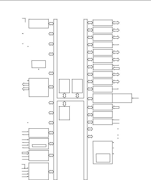
CHAPTER 1 OUTLINE
1.6 Block Diagram
RxD6/P113,
RxD6/P12 (LINSEL)
TI000/P33  16-bit TIMER/
TO00/TI010/P34 
 EVENT COUNTER 00
TOH0/P32 |
|
|
|
|
|
8-bit TIMER H0 |
|||||
|
|
|
|
||||||||
TOH1/P31 |
|
|
|
|
|
|
|
|
|
||
|
|
|
|
|
|
|
|
|
|||
|
|
|
|
|
8-bit TIMER H1 |
||||||
|
|
|
|
||||||||
|
|
|
|
|
|
|
|
|
|
|
|
|
|
|
|
|
|
|
|
|
|
|
|
|
|
|
|
|
|
|
|
|
|
|
|
|
|
|
|
|
|
|
|
|
8-bit TIMER H2 |
||
|
|
|
|
|
|
|
|
|
|
|
|
|
|
|
|
|
|
|
|
|
INTERNAL |
||
|
|
|
|
|
|
|
|
|
LOW-SPEED |
||
|
|
|
|
|
|
|
|
|
OSCILLATOR |
||
|
|
|
|
|
|
|
|
|
|||
|
|
|
|
|
|
|
|
|
|
|
|
|
|
|
|
|
|
|
|
|
|
|
|
|
|
|
|
|
|
|
|
|
|
|
|
|
|
|
|
|
|
|
WATCHDOG TIMER |
||||
|
|
|
|
|
|
|
|
|
|
|
|
|
|
|
|
|
|
|
|
|
LCD |
||
|
|
|
|
|
|
|
|
|
|||
SEG0 to SEG21 |
22 |
|
|
|
CONTROLLER |
||||||
|
|
|
|
DRIVER |
|||||||
|
|
|
|
|
|
|
|
|
|||
COM0 to COM7 |
8 |
|
|
|
|
|
|
|
|
||
|
|
|
|
|
RAM SPACE |
|
|||||
VLC0 to VLC3 |
|
|
|
|
|
|
|
FOR |
|
||
|
|
|
|
|
|||||||
|
|
|
|
|
|
|
|
|
LCD DATA |
|
|
|
|
|
|
|
|
|
|
|
|
|
|
|
|
|
|
|
|
|
8-bit TIMER/ |
||||
|
|
|
|
|
|
|
EVENT COUNTER 50 |
||||
|
|
|
|
|
|
|
|
|
|
|
|
|
|
|
|
|
|
|
|
|
|
|
|
|
|
|
|
|
|
|
8-bit TIMER/ |
||||
|
|
|
|
|
|
|
EVENT COUNTER 51 |
||||
|
|
|
|
|
|
|
|
|
|
|
|
|
|
|
|
|
|
|
|
|
|
|
|
TI52/P34 |
|
|
|
|
|
|
8-bit TIMER/ |
||||
|
|
|
|
|
|
EVENT COUNTER 52 |
|||||
|
|
|
|
|
|
|
|||||
|
|
|
|
|
|
|
|
|
|
|
|
RxD0/P12 |
|
SERIAL |
TxD0/P13 |
|
INTERFACE UART0 |
RxD6/P113 |
|
SERIAL |
TxD6/P112 |
|
|
|
INTERFACE UART6 |
|
RxD6/P12 |
|
LINSEL |
TxD6/P13 |
|
|
|
|
|
ANI0/P20 to ANI5/P25 |
6 |
10-bit |
AVREF |
|
A/D CONVERTERNote |
|
|
|
AVSS |
|
|
RxD6/P113, |
|
|
RxD6/P12 (LINSEL) |
|
|
INTP0/P120 |
|
INTERRUPT |
INTP1/P34 |
|
|
INTP2/P33 |
|
CONTROL |
|
|
|
INTP3/P31 |
|
|
|
PORT 1 |
2 |
P12, P13 |
|
|
PORT 2 |
6 |
P20 to P25 |
|
|
PORT 3 |
4 |
P31 to P34 |
|
|
PORT 4 |
|
P40 |
|
|
PORT 10 |
2 |
P100, P101 |
|
|
PORT 11 |
2 |
P112, P113 |
|
|
PORT 12 |
|
P120 |
|
|
4 |
P121 to P124 |
|
|
|
|
|
||
|
PORT 14 |
4 |
P140 to P143 |
|
78K/0 |
PORT 15 |
4 |
P150 to P153 |
|
FLASH |
|
|
|
|
CPU |
|
|
|
|
MEMORY |
|
|
|
|
CORE |
|
|
|
|
BUZZER OUTPUT |
|
BUZ/P33 |
|
|
|
POWER ON CLEAR/ |
|
POC/LVI |
|
|
LOW VOLTAGE |
|
EXLVI/P120 |
|
|
|
CONTROL |
||
|
INDICATOR |
|
|
|
|
|
|
|
|
|
KEY RETURN |
3 |
KR0/P40, KR3/P12, KR4/P13 |
|
INTERNAL |
|
|
|
|
HIGH-SPEED |
RESET CONTROL |
|
|
|
RAM |
|
|
|
|
|
|
|
|
|
|
ON-CHIP DEBUG |
|
OCD0A/X1 |
|
|
|
OCD0B/X2 |
|
|
|
|
|
|
|
|
|
|
|
MANCHESTER |
|
|
|
|
|
|
MCGO/P32 |
|
|
|
|
|
CODE GENERATOR |
|
|
|
|
|
|
||
|
|
|
|
|
|
|
|
|
|
|
|
|
|
|
|
|
|
|
|
|
|
|
|
RTCDIV/RTCCL/P33 |
|
|
|
|
|
REAL TIME |
|
|
|
|
|
|
||
|
|
|
|
|
|
|
||||||
|
|
|
|
COUNTER |
|
|
|
|
|
|
RTC1HZ/P34 |
|
|
|
|
|
|
|
|
||||||
|
|
|
|
|
|
|
|
|
|
|
|
|
|
|
|
|
|
|
|
|
|
|
|
RESET |
|
|
|
|
|
|
|
|
|
|
||||
|
|
|
|
SYSTEM |
|
|
|
|
|
|
X1/P121 |
|
|
|
|
|
|
|
|
|
|||||
|
|
|
|
|
|
|
|
|
|
X2/EXCLK/P122 |
||
|
|
|
|
CONTROL |
|
|
|
|
|
|
||
|
|
|
|
|
|
|
|
|
|
XT1/P123 |
||
|
|
|
|
|
|
|
|
|
|
|
||
|
|
|
|
|
|
|
|
|
|
|||
VDD VSS FLMD0 |
|
|
|
|
|
|
XT2/P124 |
|||||
|
|
|
|
|
|
|||||||
|
|
|
|
INTERNAL |
|
|
|
|
|
|
|
|
|
|
|
|
HIGH-SPEED |
|
|
|
|
|
|
|
|
|
|
|
|
OSCILLATOR |
|
|
|
|
|
|
|
|
|
|
|
|
|
|
|
|
|
|
|
|
|
|
|
|
|
VOLTAGE |
|
|
|
|
|
|
REGC |
|
|
|
|
|
REGULATOR |
|
|
|
|
|
|
||
|
|
|
|
|
|
|
|
|
|
|
|
|
Note μPD78F041x only.
User’s Manual U18698EJ1V0UD |
23 |

CHAPTER 1 OUTLINE
1.7 Outline of Functions
|
|
|
|
|
|
|
|
|
|
(1/2) |
|
|
Item |
|
|
μPD78F0400 |
|
μPD78F0401 |
μPD78F0402 |
μPD78F0403 |
|
|
|
|
|
|
μPD78F0410 |
|
μPD78F0411 |
μPD78F0412 |
μPD78F0413 |
|
Internal |
|
Flash memory |
8 KB |
|
16 KB |
24 KB |
32 KB |
|||
memory |
|
(self-programming |
|
|
|
|
|
|
|
|
|
|
supported)Note |
|
|
|
|
|
|
|
|
|
|
High-speed RAMNote |
512 bytes |
|
768 bytes |
1 KB |
|
|||
|
|
LCD display RAM |
22 × 4 bits (with 4 com) or 18 × 8 bits (with 8 com) |
|
||||||
Memory space |
64 KB |
|
|
|
|
|||||
Main system |
|
High-speed system |
X1 (crystal/ceramic) oscillation, external main system clock input (EXCLK) |
|||||||
clock |
|
clock |
|
|
2 to 10 MHz: VDD = 2.7 to 5.5 V, |
|
|
|||
(oscillation |
|
|
|
|
2 to 5 MHz: VDD = 1.8 to 5.5 V |
|
|
|||
frequency) |
|
Internal high-speed |
Internal oscillation |
|
|
|
|
|||
|
|
|
|
|
|
|||||
|
|
oscillation clock |
|
|
8 MHz (TYP.): VDD = 1.8 to 5.5 V |
|
|
|||
Subsystem clock |
XT1 (crystal) oscillation |
|
|
|
|
|||||
(oscillation frequency) |
|
|
32.768 kHz (TYP.): VDD = 1.8 to 5.5 V |
|
|
|||||
Internal low-speed oscillation clock |
Internal oscillation |
|
|
|
|
|||||
(for TMH1, WDT) |
|
|
240 kHz (TYP.): VDD = 1.8 to 5.5 V |
|
|
|||||
General-purpose registers |
8 bits × 32 registers (8 bits × 8 registers × 4 banks) |
|
||||||||
Minimum instruction execution time |
0.2 μs (high-speed system clock: @ fXH = 10 MHz operation) |
|
||||||||
|
|
|
0.25 μs (internal high-speed oscillation clock: @ fRH = 8 MHz (TYP.) operation) |
|||||||
|
|
|
122 μs (subsystem clock: @ fSUB = 32.768 kHz operation) |
|
||||||
Instruction set |
|
• |
8-bit operation and 16-bit operation |
|
|
|||||
|
|
|
• |
Bit manipulate (set, reset, test, and Boolean operation) |
|
|||||
|
|
|
• |
BCD adjust, etc. |
|
|
|
|
||
I/O ports |
|
|
Total: |
30 |
|
|
|
|||
|
|
|
|
CMOS I/O: |
26 |
|
|
|
||
|
|
|
|
CMOS input: |
4 |
|
|
|
||
|
|
|
|
|
||||||
Timers |
|
• 16-bit timer/event counter: 1 channels |
|
|
||||||
|
|
|
• 8-bit timer/event counter: 3 channels |
|
|
|||||
|
|
|
• 8-bit timer: 3 channels (out of which 2 channels can perform PWM output) |
|||||||
|
|
|
• Real-time counter: 1 channel |
|
|
|||||
|
|
|
• Watchdog timer: 1 channel |
|
|
|||||
|
|
Timer outputs |
3 (PWM output: 2 and PPG output: 1) |
|
|
|||||
|
|
RTC outputs |
2 |
|
|
|
|
|
|
|
|
|
|
• |
1 Hz (Subsystem clock: fSUB = 32.768 kHz) |
|
|
||||
|
|
|
• |
512 Hz or 16.384 kHz or 32.768 kHz (Subsystem clock: fSUB = 32.768 kHz) |
||||||
Buzzer output |
|
• 1.22 kHz, 2.44 kHz, 4.88 kHz, 9.77 MHz |
|
|
||||||
|
|
|
|
|
(peripheral hardware clock: @ fPRS = 10 MHz operation) |
|
||||
Note The internal flash memory capacity and internal high-speed RAM capacity can be changed using the internal memory size switching register (IMS).
24 |
User’s Manual U18698EJ1V0UD |

CHAPTER 1 OUTLINE
|
|
|
|
|
|
|
|
|
|
|
|
(2/2) |
|
Item |
|
μPD78F0400 |
|
μPD78F0401 |
μPD78F0402 |
|
μPD78F0403 |
||||
|
|
|
|
μPD78F0410 |
|
μPD78F0411 |
μPD78F0412 |
|
μPD78F0413 |
|||
10-bit successive approximation |
• μPD78F040x: None |
|
|
|
|
|||||||
type A/D converter |
• μPD78F041x: 6 channels |
|
|
|
|
|||||||
|
|
|
|
|
|
|
||||||
Serial interface |
|
|
• UART supporting LIN-busNote 1: 1 channel |
|
|
|
||||||
|
|
|
• UART: 1 channel |
|
|
|
|
|||||
LCD controller/driver |
• External resistance division and internal resistance division are switchable. |
|
||||||||||
|
|
|
• Segment signal outputs: 22 (18)Note 2 |
|
|
|
||||||
|
|
|
• Common signal outputs: 4 (8)Note 2 |
|
|
|
||||||
Manchester code generator |
Provided |
|
|
|
|
|
|
|
||||
Vectored |
|
Internal |
• μPD78F040x: |
17 |
|
|
|
|
|
|
||
interrupt sources |
|
• μPD78F041x: |
18 |
|
|
|
|
|
|
|||
|
|
External |
5 |
|
|
|
|
|
|
|
|
|
Key interrupt |
|
|
Key interrupt (INTKR) occurs by detecting falling edge of key input pins (KR0, KR3, KR4). |
|||||||||
Reset |
|
|
• Reset using |
|
pin |
|
|
|
|
|||
|
|
RESET |
|
|
|
|
||||||
|
|
|
• |
Internal reset by watchdog timer |
|
|
|
|||||
|
|
|
• |
Internal reset by power-on-clear |
|
|
|
|||||
|
|
|
• |
Internal reset by low-voltage detector |
|
|
|
|||||
On-chip debug function |
Provided |
|
|
|
|
|
|
|
||||
Power supply voltage |
VDD = 1.8 to 5.5 V |
|
|
|
|
|||||||
Operating ambient temperature |
TA = −40 to +85°C |
|
|
|
|
|||||||
Package |
|
|
48-pin plastic LQFP (fine pitch) (7 × 7) |
|
|
|
||||||
Notes 1. The LIN-bus supporting UART pins can be changed to the UART pins (pin numbers 47 and 48). 2. The values in parentheses are the number of signal outputs when 8com is used.
User’s Manual U18698EJ1V0UD |
25 |
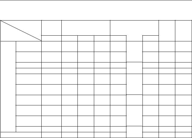
CHAPTER 1 OUTLINE
An outline of the timer is shown below.
|
|
16-Bit Timer/ |
|
8-Bit Timer/ |
|
8-Bit Timers H0, H1, and H2 |
Real-time |
Watchdog |
||
|
|
Event |
Event Counters 50, 51, and 52 |
|
|
|
Counter |
Timer |
||
|
|
Counters 00 |
|
|
|
|
|
|
|
|
|
|
TM00 |
TM50 |
TM51 |
TM52 |
TMH0 |
TMH1 |
TMH2 |
|
|
Function |
Interval timer |
1 channel |
1 channel |
1 channel |
1 channel |
1 channel |
1 channel |
1 channel |
1 channel |
− |
|
|
|
|
|
|
|
|
|
Note 1 |
|
|
External event |
1 channel |
− |
− |
1 channel |
− |
− |
−Note 2 |
− |
− |
|
counter |
Note 2 |
|
|
Note 2 |
|
|
|
|
|
|
|
|
|
|
|
|
|
|
|
|
|
PPG output |
1 output |
− |
− |
− |
− |
− |
− |
− |
− |
|
PWM output |
− |
− |
− |
− |
1 output |
1 output |
− |
− |
− |
|
Pulse width |
2 inputs |
− |
− |
− |
− |
− |
− |
− |
− |
|
measurement |
|
|
|
|
|
|
|
|
|
|
Square-wave |
1 output |
− |
− |
− |
1 output |
1 output |
− |
− |
− |
|
output |
|
|
|
|
|
|
|
|
|
|
Carrier |
− |
− |
−Note 3 |
− |
− |
1 output |
− |
− |
− |
|
generator |
|
|
|
|
|
Note 3 |
|
|
|
|
|
|
|
|
|
|
|
|
|
|
|
Calendar |
− |
− |
− |
− |
− |
− |
− |
1 channel |
|
|
function |
|
|
|
|
|
|
|
Note 1 |
|
|
|
|
|
|
|
|
|
|
|
|
|
RTC output |
− |
− |
− |
− |
− |
− |
− |
2 outputs |
− |
|
|
|
|
|
|
|
|
|
Note 4 |
|
|
Watchdog timer |
− |
− |
− |
− |
− |
− |
− |
− |
1 channel |
Interrupt source |
2 |
1 |
1 |
1 |
1 |
1 |
1 |
1 |
− |
|
Notes 1. |
In the real-time counter, the Interval timer function and calendar function can be used simultaneously. |
|||||||||
2.TM52 and TM00 can be connected in cascade to be used as a 24-bit counter. Also, the external event input of TM52 can be input enable-controlled via TMH2.
3.TM51 and TMH1 can be used in combination as a carrier generator mode.
4.A 1 Hz output can be used as one output and a 512 Hz, 16.384 kHz, or 32.768 kHz output can be used as one output.
26 |
User’s Manual U18698EJ1V0UD |
CHAPTER 2 PIN FUNCTIONS
2.1 Pin Function List
There are three types of pin I/O buffer power supplies: AVREFNote, VLC0, and VDD. The relationship between these power supplies and the pins is shown below.
Table 2-1. Pin I/O Buffer Power Supplies
Power Supply |
Corresponding Pins |
|
|
AVREFNote |
P20 to P25 |
VLC0 |
COM0 to COM7, SEG0 to SEG21, VLC0 to VLC3 |
|
|
VDD |
Pins other than above |
|
|
Note μPD78F041x only. The power supply is VDD with μPD78F040x. |
|
|
|
||
(1) Port pins |
|
|
|
|
(1/2) |
|
|
|
|
|
|
Function Name |
I/O |
Function |
After Reset |
Alternate Function |
|
P12 |
I/O |
Port 1. |
Input port |
RxD0/KR3/<RxD6> |
|
|
|
2-bit I/O port. |
|
|
|
P13 |
|
|
TxD0/KR4/<TxD6> |
||
|
Input/output can be specified in 1-bit units. |
|
|||
|
|
|
|
|
|
|
|
Use of an on-chip pull-up resistor can be specified by a |
|
|
|
|
|
software setting. |
|
|
|
|
|
|
|
|
|
P20 |
I/O |
Port 2. |
Digital |
SEG21/ANI0Note |
|
P21 |
|
6-bit I/O port. |
input port |
SEG20/ANI1 |
Note |
|
Input/output can be specified in 1-bit units. |
|
|
||
|
|
|
|
|
|
P22 |
|
|
SEG19/ANI2Note |
||
|
|
|
|||
P23 |
|
|
|
SEG18/ANI3Note |
|
P24 |
|
|
|
SEG17/ANI4Note |
|
P25 |
|
|
|
SEG16/ANI5Note |
|
P31 |
I/O |
Port 3. |
Input port |
TOH1/INTP3 |
|
|
|
4-bit I/O port. |
|
|
|
P32 |
|
|
TOH0/MCGO |
||
|
Input/output can be specified in 1-bit units. |
|
|||
|
|
|
|
|
|
P33 |
|
|
TI000/RTCDIV/ |
||
|
Use of an on-chip pull-up resistor can be specified by a |
|
|||
|
|
|
RTCCL/BUZ/INTP2 |
||
|
|
software setting. |
|
||
|
|
|
|
|
|
P34 |
|
|
TI52/TI010/TO00/ |
||
|
|
|
|||
|
|
|
|
RTC1HZ/INTP1 |
|
|
|
|
|
|
|
P40 |
I/O |
Port 4. |
Input port |
VLC3/KR0 |
|
|
|
1-bit I/O port. |
|
|
|
|
|
Input/output can be specified in 1-bit units. |
|
|
|
|
|
Use of an on-chip pull-up resistor can be specified by a |
|
|
|
|
|
software setting. |
|
|
|
|
|
|
|
|
|
Note μPD78F041x only.
Remark The functions within arrowheads (< >) can be assigned by setting the input switch control register (ISC).
User’s Manual U18698EJ1V0UD |
27 |

CHAPTER 2 PIN FUNCTIONS
(1) Port pins |
|
|
|
(2/2) |
|
|
|
|
|
Function Name |
I/O |
Function |
After Reset |
Alternate Function |
|
|
|
|
|
P100, P101 |
I/O |
Port 10. |
Input port |
SEG4, SEG5 |
|
|
2-bit I/O port. |
|
|
|
|
Input/output can be specified in 1-bit units. |
|
|
|
|
Use of an on-chip pull-up resistor can be specified by a |
|
|
|
|
software setting. |
|
|
|
|
|
|
|
P112 |
I/O |
Port 11. |
Input port |
SEG6/TxD6 |
|
|
2-bit I/O port. |
|
|
P113 |
|
|
SEG7/RxD6 |
|
|
Input/output can be specified in 1-bit units. |
|
||
|
|
|
|
|
|
|
Use of an on-chip pull-up resistor can be specified by a |
|
|
|
|
software setting. |
|
|
|
|
|
|
|
P120 |
I/O |
Port 12. |
Input port |
INTP0/EXLVI |
P121 |
Input |
1-bit I/O port and 4-bit input port. |
|
X1/OCD0A |
Only for P120, use of an on-chip pull-up resistor can be |
|
|||
|
|
|
|
|
P122 |
|
|
X2/EXCLK/OCD0B |
|
|
specified by a software setting. |
|
||
|
|
|
|
|
P123 |
|
|
XT1 |
|
|
|
|
||
P124 |
|
|
|
XT2 |
|
|
|
|
|
P140 to P143 |
I/O |
Port 14. |
Input port |
SEG8 to SEG11 |
|
|
4-bit I/O port. |
|
|
|
|
Input/output can be specified in 1-bit units. |
|
|
|
|
Use of an on-chip pull-up resistor can be specified by a |
|
|
|
|
software setting. |
|
|
|
|
|
|
|
P150 to P153 |
I/O |
Port 15. |
Input port |
SEG12 to SEG15 |
|
|
4-bit I/O port. |
|
|
|
|
Input/output can be specified in 1-bit units. |
|
|
|
|
Use of an on-chip pull-up resistor can be specified by a |
|
|
|
|
software setting. |
|
|
28 |
User’s Manual U18698EJ1V0UD |

CHAPTER 2 PIN FUNCTIONS
(2) Non-port pins |
|
|
|
(1/2) |
||
|
|
|
|
|
||
Function Name |
I/O |
Function |
After Reset |
Alternate Function |
||
|
|
|
|
|
||
ANI0Note |
Input |
10-bit successive approximation type A/D converter |
Digital input |
P20/SEG21 |
||
ANI1 |
Note |
|
analog input. |
port |
P21/SEG20 |
|
|
|
|
|
|||
|
|
|
|
|
||
ANI2Note |
|
|
|
P22/SEG19 |
||
ANI3Note |
|
|
|
P23/SEG18 |
||
ANI4Note |
|
|
|
P24/SEG17 |
||
ANI5Note |
|
|
|
P25/SEG16 |
||
AVREFNote |
Input |
10-bit successive approximation type A/D converter |
− |
− |
||
|
|
|
reference voltage input, positive power supply for port 2 |
|
|
|
|
|
|
|
|
||
AVSSNote |
− |
A/D converter ground potential. Make the same potential as |
− |
− |
||
|
|
|
VSS. |
|
|
|
|
|
|
|
|
||
SEG0 to SEG3 |
Output |
LCD controller/driver segment signal outputs |
Output |
COM4 to COM7 |
||
SEG4, SEG5 |
|
|
Input port |
P100, P101 |
||
|
|
|
|
|
||
SEG6 |
|
|
|
P112/TxD6 |
||
|
|
|
|
|
||
SEG7 |
|
|
|
P113/RxD6 |
||
SEG8 to SEG11 |
|
|
|
P114 to P143 |
||
|
|
|
|
|
||
SEG12 to SEG15 |
|
|
|
P150 to P153 |
||
|
|
|
|
|
||
SEG16 |
|
|
Digital input |
P25/ANI5Note |
||
SEG17 |
|
|
port |
P24/ANI4 |
Note |
|
|
|
|
|
|||
|
|
|
|
|
||
SEG18 |
|
|
|
P23/ANI3Note |
||
SEG19 |
|
|
|
P22/ANI2Note |
||
SEG20 |
|
|
|
P21/ANI1Note |
||
SEG21 |
|
|
|
P20/ANI0Note |
||
COM0 to COM3 |
Output |
LCD controller/driver common signal outputs |
Output |
− |
||
COM4 to COM7 |
|
|
|
SEG0 to SEG3 |
||
|
|
|
|
|
||
VLC0 to VLC2 |
− |
LCD drive voltage |
− |
− |
||
|
|
|
|
|
|
|
VLC3 |
|
|
|
Input port |
P40/KR0 |
|
BUZ |
|
Output |
Buzzer output |
Input port |
P33/TI000/RTCDIV/ |
|
|
|
|
|
|
RTCCL/INTP2 |
|
|
|
|
|
|
||
INTP0 |
Input |
External interrupt request input for which the valid edge |
Input port |
P120/EXLVI |
||
|
|
|
(rising edge, falling edge, or both rising and falling edges) |
|
|
|
INTP1 |
|
|
P34/TI52/TI010/ |
|||
|
can be specified |
|
||||
|
|
|
|
TO00/RTC1HZ |
||
|
|
|
|
|
||
INTP2 |
|
|
|
P33/TI000/RTCDIV/ |
||
|
|
|
|
|
RTCCL/BUZ |
|
|
|
|
|
|
||
INTP3 |
|
|
|
P31/TOH1 |
||
|
|
|
|
|
|
|
KR0 |
|
Input |
Key interrupt input |
Input port |
P40/VLC3 |
|
KR3 |
|
|
|
|
P12/RxD0/<RxD6> |
|
|
|
|
|
|
|
|
KR4 |
|
|
|
|
P13/TxD0/<TxD6> |
|
|
|
|
|
|
||
MCGO |
Output |
Manchester code output |
Input port |
P32/TOH0 |
||
Note μPD78F041x only.
Remark The functions within arrowheads (< >) can be assigned by setting the input switch control register (ISC).
User’s Manual U18698EJ1V0UD |
29 |

CHAPTER 2 PIN FUNCTIONS
(2) Non-port pins |
|
|
(2/2) |
|||
|
|
|
|
|
|
|
|
Function Name |
I/O |
Function |
After Reset |
Alternate Function |
|
|
|
|
|
|
|
|
|
|
|
Input |
System reset input |
− |
− |
RESET |
||||||
|
|
|
|
|
|
|
RTCDIV |
Output |
Real-time counter clock (32 kHz divided frequency) output |
Input port |
P33/TI000/RTCCL |
||
|
|
|
|
|
|
/BUZ/INTP2 |
|
|
|
|
|
|
|
RTCCL |
Output |
Real-time counter clock (32 kHz original oscillation) output |
Input port |
P33/TI000/RTCDIV |
||
|
|
|
|
|
|
/BUZ/INTP2 |
RTC1HZ |
Output |
Real-time counter clock (1 Hz) output |
Input port |
P34/TI52/TI010/ |
||
|
|
|
|
|
|
TO00/INTP1 |
|
|
|
|
|
|
|
RxD0 |
Input |
Serial data input to asynchronous serial interface |
Input port |
P12/KR3/<RxD6> |
||
|
|
|
|
|
|
|
RxD6 |
|
|
|
P113/SEG7 |
||
<RxD6> |
|
|
|
P12/RxD0/KR3 |
||
|
|
|
|
|
|
|
TI000 |
Input |
External count clock input to 16-bit timer/event counter 00 |
Input port |
P33/RTCDIV/ |
||
|
|
|
|
Capture trigger input to capture registers (CR000, CR010) of |
|
RTCCL/BUZ/ |
|
|
|
|
16-bit timer/event counter 00 |
|
INTP2 |
|
|
|
|
|
|
|
TI010 |
|
Capture trigger input to capture register (CR000) of 16-bit |
|
P34/TI52/TO00/ |
||
|
|
|
|
timer/event counter 00 |
|
RTC1HZ/INTP1 |
TI52 |
Input |
External count clock input to 8-bit timer/event counter 52 |
Input port |
P34/TI010/TO00/ |
||
|
|
|
|
|
|
RTC1HZ/INTP1 |
|
|
|
|
|
|
|
TO00 |
Output |
16-bit timer/event counter 00 output |
Input port |
P34/TI52/TI010/ |
||
|
|
|
|
|
|
RTC1HZ/INTP1 |
|
|
|
|
|
|
|
TOH0 |
Output |
8-bit timer H0 output |
Input port |
P32/MCGO |
||
TOH1 |
|
8-bit timer H1 output |
|
P31/INTP3 |
||
|
|
|
|
|
|
|
TxD0 |
Output |
Serial data output from asynchronous serial interface |
Input port |
P13/KR4/<TxD6> |
||
|
|
|
|
|
|
|
TxD6 |
|
|
|
P112/SEG6 |
||
<TxD6> |
|
|
|
P13/TxD0/KR4 |
||
|
|
|
|
|
|
|
EXLVI |
Input |
Potential input for external low-voltage detection |
Input port |
P120/INTP0 |
||
|
|
|
|
|
|
|
X1 |
Input |
Connecting resonator for main system clock |
Input port |
P121/OCD0A |
||
X2 |
− |
|
|
P122/EXCLK/ |
||
|
|
|
|
|
|
OCD0B |
|
|
|
|
|
|
|
EXCLK |
Input |
External clock input for main system clock |
Input port |
P122/X2/OCD0B |
||
|
|
|
|
|
|
|
XT1 |
Input |
Connecting resonator for subsystem clock |
Input port |
P123 |
||
XT2 |
− |
|
|
P124 |
||
|
|
|
|
|
|
|
VDD |
− |
Positive power supply |
− |
− |
||
|
|
|
|
|
|
|
VSS |
− |
Ground potential |
− |
− |
||
FLMD0 |
− |
Flash memory programming mode setting |
− |
− |
||
|
|
|
|
|
|
|
OCD0A |
Input |
On-chip debug mode setting connection |
Input port |
P121/X1 |
||
|
|
|
|
|
|
|
OCD0B |
− |
|
|
P122/X2/EXCLK |
||
Remark The functions within arrowheads (< >) can be assigned by setting the input switch control register (ISC).
30 |
User’s Manual U18698EJ1V0UD |
Loading...