


 Loading...
NEC PD78F0500, PD78F0501, PD78F0502, PD78F0503, PD78F0503D User Manual
...User’s Manual
78K0/Kx2
8-Bit Single-Chip Microcontrollers
Flash Memory Self Programming
µPD78F0500 |
µPD78F0521 |
µPD78F0544 |
µPD78F0501 |
µPD78F0522 |
µPD78F0545 |
µPD78F0502 |
µPD78F0523 |
µPD78F0546 |
µPD78F0503 |
µPD78F0524 |
µPD78F0547 |
µPD78F0503D |
µPD78F0525 |
µPD78F0547D |
µPD78F0511 |
µPD78F0526 |
|
µPD78F0512 |
µPD78F0527 |
|
µPD78F0513 |
µPD78F0527D |
|
µPD78F0513D |
µPD78F0531 |
|
µPD78F0514 |
µPD78F0532 |
|
µPD78F0515 |
µPD78F0533 |
|
µPD78F0515D |
µPD78F0534 |
|
|
µPD78F0535 |
|
|
µPD78F0536 |
|
|
µPD78F0537 |
|
|
µPD78F0537D |
|
Document No. U17516EJ1V0UM00 (1st edition)
Date Published August 2005 N CP(K)


 2005
2005
Printed in Japan
[MEMO]
2
User’s Manual U17516EJ1V0UM

NOTES FOR CMOS DEVICES
1VOLTAGE APPLICATION WAVEFORM AT INPUT PIN
Waveform distortion due to input noise or a reflected wave may cause malfunction. If the input of the CMOS device stays in the area between VIL (MAX) and VIH (MIN) due to noise, etc., the device may malfunction. Take care to prevent chattering noise from entering the device when the input level is fixed, and also in the transition period when the input level passes through the area between VIL (MAX) and VIH (MIN).
2HANDLING OF UNUSED INPUT PINS
Unconnected CMOS device inputs can be cause of malfunction. If an input pin is unconnected, it is possible that an internal input level may be generated due to noise, etc., causing malfunction. CMOS devices behave differently than Bipolar or NMOS devices. Input levels of CMOS devices must be fixed high or low by using pull-up or pull-down circuitry. Each unused pin should be connected to VDD or GND via a resistor if there is a possibility that it will be an output pin. All handling related to unused pins must be judged separately for each device and according to related specifications governing the device.
3PRECAUTION AGAINST ESD
A strong electric field, when exposed to a MOS device, can cause destruction of the gate oxide and ultimately degrade the device operation. Steps must be taken to stop generation of static electricity as much as possible, and quickly dissipate it when it has occurred. Environmental control must be adequate. When it is dry, a humidifier should be used. It is recommended to avoid using insulators that easily build up static electricity. Semiconductor devices must be stored and transported in an anti-static container, static shielding bag or conductive material. All test and measurement tools including work benches and floors should be grounded. The operator should be grounded using a wrist strap. Semiconductor devices must not be touched with bare hands. Similar precautions need to be taken for PW boards with mounted semiconductor devices.
4STATUS BEFORE INITIALIZATION
Power-on does not necessarily define the initial status of a MOS device. Immediately after the power source is turned ON, devices with reset functions have not yet been initialized. Hence, power-on does not guarantee output pin levels, I/O settings or contents of registers. A device is not initialized until the reset signal is received. A reset operation must be executed immediately after power-on for devices with reset functions.
5POWER ON/OFF SEQUENCE
In the case of a device that uses different power supplies for the internal operation and external interface, as a rule, switch on the external power supply after switching on the internal power supply. When switching the power supply off, as a rule, switch off the external power supply and then the internal power supply. Use of the reverse power on/off sequences may result in the application of an overvoltage to the internal elements of the device, causing malfunction and degradation of internal elements due to the passage of an abnormal current.
The correct power on/off sequence must be judged separately for each device and according to related specifications governing the device.
6INPUT OF SIGNAL DURING POWER OFF STATE
Do not input signals or an I/O pull-up power supply while the device is not powered. The current injection that results from input of such a signal or I/O pull-up power supply may cause malfunction and the abnormal current that passes in the device at this time may cause degradation of internal elements. Input of signals during the power off state must be judged separately for each device and according to related specifications governing the device.
User’s Manual U17516EJ1V0UM |
3 |

•The information in this document is current as of July, 2005. The information is subject to change without notice. For actual design-in, refer to the latest publications of NEC Electronics data sheets or data books, etc., for the most up-to-date specifications of NEC Electronics products. Not all products and/or types are available in every country. Please check with an NEC Electronics sales representative for availability and additional information.
•No part of this document may be copied or reproduced in any form or by any means without the prior written consent of NEC Electronics. NEC Electronics assumes no responsibility for any errors that may appear in this document.
•NEC Electronics does not assume any liability for infringement of patents, copyrights or other intellectual property rights of third parties by or arising from the use of NEC Electronics products listed in this document or any other liability arising from the use of such products. No license, express, implied or otherwise, is granted under any patents, copyrights or other intellectual property rights of NEC Electronics or others.
•Descriptions of circuits, software and other related information in this document are provided for illustrative purposes in semiconductor product operation and application examples. The incorporation of these circuits, software and information in the design of a customer's equipment shall be done under the full responsibility of the customer. NEC Electronics assumes no responsibility for any losses incurred by customers or third parties arising from the use of these circuits, software and information.
•While NEC Electronics endeavors to enhance the quality, reliability and safety of NEC Electronics products, customers agree and acknowledge that the possibility of defects thereof cannot be eliminated entirely. To minimize risks of damage to property or injury (including death) to persons arising from defects in NEC Electronics products, customers must incorporate sufficient safety measures in their design, such as redundancy, fire-containment and anti-failure features.
•NEC Electronics products are classified into the following three quality grades: "Standard", "Special" and "Specific".
The "Specific" quality grade applies only to NEC Electronics products developed based on a customerdesignated "quality assurance program" for a specific application. The recommended applications of an NEC Electronics product depend on its quality grade, as indicated below. Customers must check the quality grade of each NEC Electronics product before using it in a particular application.
"Standard": Computers, office equipment, communications equipment, test and measurement equipment, audio and visual equipment, home electronic appliances, machine tools, personal electronic equipment and industrial robots.
"Special": Transportation equipment (automobiles, trains, ships, etc.), traffic control systems, anti-disaster systems, anti-crime systems, safety equipment and medical equipment (not specifically designed for life support).
"Specific": Aircraft, aerospace equipment, submersible repeaters, nuclear reactor control systems, life support systems and medical equipment for life support, etc.
The quality grade of NEC Electronics products is "Standard" unless otherwise expressly specified in NEC Electronics data sheets or data books, etc. If customers wish to use NEC Electronics products in applications not intended by NEC Electronics, they must contact an NEC Electronics sales representative in advance to determine NEC Electronics' willingness to support a given application.
(Note)
(1)"NEC Electronics" as used in this statement means NEC Electronics Corporation and also includes its majority-owned subsidiaries.
(2)"NEC Electronics products" means any product developed or manufactured by or for NEC Electronics (as defined above).
M8E 02. 11-1
4 |
User’s Manual U17516EJ1V0UM |
Regional Information
Some information contained in this document may vary from country to country. Before using any NEC Electronics product in your application, pIease contact the NEC Electronics office in your country to obtain a list of authorized representatives and distributors. They will verify:
•Device availability
•Ordering information
•Product release schedule
•Availability of related technical literature
•Development environment specifications (for example, specifications for third-party tools and components, host computers, power plugs, AC supply voltages, and so forth)
•Network requirements
In addition, trademarks, registered trademarks, export restrictions, and other legal issues may also vary from country to country.
[GLOBAL SUPPORT] http://www.necel.com/en/support/support.html
NEC Electronics America, Inc. (U.S.) |
NEC Electronics (Europe) GmbH |
NEC Electronics Hong Kong Ltd. |
Santa Clara, California |
Duesseldorf, Germany |
Hong Kong |
Tel: 408-588-6000 |
Tel: 0211-65030 |
Tel: 2886-9318 |
800-366-9782 |
|
NEC Electronics Hong Kong Ltd. |
|
• Sucursal en España |
|
|
Madrid, Spain |
Seoul Branch |
|
Tel: 091-504 27 87 |
Seoul, Korea |
|
• Succursale Française |
Tel: 02-558-3737 |
|
|
|
|
Vélizy-Villacoublay, France |
NEC Electronics Shanghai Ltd. |
|
Tel: 01-30-67 58 00 |
Shanghai, P.R. China |
|
|
|
|
• Filiale Italiana |
Tel: 021-5888-5400 |
|
|
|
|
Milano, Italy |
NEC Electronics Taiwan Ltd. |
|
Tel: 02-66 75 41 |
|
|
Taipei, Taiwan |
|
|
|
|
|
• Branch The Netherlands |
Tel: 02-2719-2377 |
|
|
|
|
Eindhoven, The Netherlands |
NEC Electronics Singapore Pte. Ltd. |
|
Tel: 040-265 40 10 |
|
|
Novena Square, Singapore |
|
|
|
|
|
• Tyskland Filial |
Tel: 6253-8311 |
|
Taeby, Sweden |
|
|
Tel: 08-63 87 200 |
|
|
• United Kingdom Branch |
|
|
Milton Keynes, UK |
|
|
Tel: 01908-691-133 |
|
J05.6
User’s Manual U17516EJ1V0UM |
5 |
|
INTRODUCTION |
||
Readers |
This manual is intended for users who wish to understand the functions of the flash |
||
|
memory versions of the 78K0/Kx2 and design application systems using these |
||
|
microcontrollers. |
|
|
Purpose |
This manual is intended to give users an understanding of the usage of the flash |
||
|
memory self programming sample library which is used when rewriting the 78K0/Kx2 |
||
|
flash memory. |
|
|
Organization |
This manual can be generally divided into the following sections. |
||
|
• Description of flash environment |
||
|
• Description of flash memory self programming sample library |
||
How to Read This Manual |
It is assumed that the readers of this manual have general knowledge in the fields of |
||
|
electrical engineering, logic circuits, and microcontrollers. |
||
|
To check the hardware functions of the 78K0/Kx2 |
||
|
→ Refer to the user’s manual of each 78k0/Kx2 product. |
||
Conventions |
Data significance: |
Higher digits on the left and lower digits on the right |
|
|
Active low representation: |
|
(overscore over pin or signal name) |
|
xxx |
||
|
Note: |
Footnote for item marked with Note in the text |
|
|
Caution: |
Information requiring particular attention |
|
|
Remark: |
Supplementary information |
|
|
Numerical representation: Binary … xxxx or xxxxB |
||
|
|
Decimal … xxxx |
|
|
|
Hexadecimal … xxxxH |
|
6 |
User’s Manual U17516EJ1V0UM |
Terminology |
The following describes the meanings of certain terms used in this manual. |
|
|
• |
Self programming |
|
|
Self programming operations are flash memory write operations that are performed |
|
|
by user programs. |
|
• Flash memory self programming sample library |
|
|
|
This is the library that is provided by the 78K0/Kx2 for flash memory manipulation. |
|
• |
Flash environment |
|
|
This is the environment that supports flash memory manipulations. It has |
|
|
restrictions that differ from those applied to ordinary program execution. |
|
• |
Block number |
|
|
Block numbers indicate blocks in flash memory. They are used as units during |
|
|
manipulations such as erasures and blank checks. |
|
• |
Boot cluster |
|
|
This is the area that is used for boot swapping. Boot cluster 0 and boot cluster 1 |
|
|
are provided and the cluster to be booted can be selected. |
|
• |
Entry RAM |
|
|
This is the area in RAM that is used by the flash memory self programming sample |
|
|
library. The user program reserves this area and specifies the start address of the |
|
|
specific area to be used when the library is called. |
|
• |
Internal verification |
|
|
After writing to flash memory, signal levels are checked internally to confirm correct |
|
|
reading of data. When an internal verification error occurs, the corresponding |
|
|
device is judged as faulty. |
User’s Manual U17516EJ1V0UM |
7 |
CONTENTS
CHAPTER 1 GENERAL........................................................................................................................... |
11 |
|
1.1 |
Overview..................................................................................................................................... |
11 |
1.2 |
Calling Self Programming Sample Library ............................................................................. |
11 |
1.3 |
Bank Number and Block Number ............................................................................................ |
14 |
1.4 |
Processing Time and Acknowledging Interrupt ..................................................................... |
17 |
CHAPTER 2 PROGRAMMING ENVIRONMENT .................................................................................... |
20 |
|
2.1 |
Hardware Environment.............................................................................................................. |
20 |
2.2 |
Software Environment............................................................................................................... |
21 |
2.2.1 Entry RAM ........................................................................................................................................... |
22 |
|
2.2.2 Stack and data buffer........................................................................................................................... |
23 |
|
CHAPTER 3 INTERRUPT SERVICING DURING SELF PROGRAMMING ............................................ |
24 |
|
3.1 |
Overview..................................................................................................................................... |
24 |
3.2 |
Interrupt Response Time........................................................................................................... |
27 |
3.3 |
Description Example ................................................................................................................. |
29 |
3.4 |
Cautions ..................................................................................................................................... |
31 |
CHAPTER 4 BOOT SWAP FUNCTION................................................................................................... |
32 |
|
CHAPTER 5 SELF PROGRAMMING SAMPLE LIBRARY..................................................................... |
39 |
|
5.1 |
Type of Self Programming Sample Library ............................................................................. |
39 |
5.2 |
Explanation of Self Programming Sample Library................................................................. |
40 |
|
self programming start library ..................................................................................................................... |
41 |
|
initialize library ............................................................................................................................................ |
43 |
|
mode check library...................................................................................................................................... |
45 |
|
block blank check library ............................................................................................................................. |
47 |
|
block erase library....................................................................................................................................... |
51 |
|
word write library......................................................................................................................................... |
55 |
|
block verify library ....................................................................................................................................... |
60 |
|
self programming end library ...................................................................................................................... |
64 |
|
get information library ................................................................................................................................. |
66 |
|
set information library.................................................................................................................................. |
72 |
|
EEPROM write library ................................................................................................................................. |
76 |
CHAPTER 6 DETAILS OF SELF PROGRAMMING CONTROL............................................................. |
81 |
|
6.1 |
Registers That Control Self Programming .............................................................................. |
81 |
6.1.1 Flash programming mode control register (FLPMC)............................................................................ |
81 |
|
6.1.2 Flash protect command register (PFCMD) .......................................................................................... |
83 |
|
6.1.3 Flash status register (PFS) .................................................................................................................. |
84 |
|
6.1.4 Self programming control parameters.................................................................................................. |
85 |
|
APPENDIX A SAMPLE PROGRAM........................................................................................................ |
90 |
|
A.1 |
User Program ............................................................................................................................. |
90 |
A.2 |
Self Programming Library (Normal Model) ........................................................................... |
103 |
A.3 |
Self Programming Library (Static Model).............................................................................. |
118 |
A.4 |
Boot Swap ................................................................................................................................ |
132 |
A.5 |
Compiling the Flash Self Programming Sample Library and Sample Program................ |
137 |
APPENDIX B INDEX.............................................................................................................................. |
138 |
|
8 |
User’s Manual U17516EJ1V0UM |
|
|
LIST OF FIGURES |
|
Figure 1-1 |
Flow of Self Programming (rewriting contents of flash memory)....................................................... |
12 |
Figure 1-2 |
Block Numbers and Boot Clusters (flash memory of up to 60 KB) ................................................... |
15 |
Figure 1-3 |
Block Numbers and Boot Clusters (flash memory of 96 KB or more) ............................................... |
16 |
Figure 2-1 |
FLMD0 Voltage Generator ................................................................................................................ |
20 |
Figure 2-2 |
Allocation Range of Entry RAM ........................................................................................................ |
22 |
Figure 2-3 |
Allocatable Range for Stack Pointer and Data Buffer ....................................................................... |
23 |
Figure 3-1 |
Flow of Processing in Case of Interrupt............................................................................................ |
25 |
Figure 4-1 |
Flow of Boot Swapping ..................................................................................................................... |
33 |
Figure 5-1 |
Flow of Self Programming Start Library............................................................................................ |
42 |
Figure 5-2 |
Flow of Initialize Library .................................................................................................................... |
44 |
Figure 5-3 |
Flow of Mode Check Library ............................................................................................................. |
46 |
Figure 5-4 |
Flow of Block Blank Check Library ................................................................................................... |
50 |
Figure 5-5 |
Flow of Block Erase Library .............................................................................................................. |
54 |
Figure 5-6 |
Flow of Word Write Library ............................................................................................................... |
59 |
Figure 5-7 |
Flow of Block Verify Library............................................................................................................... |
63 |
Figure 5-8 |
Flow of Self Programming End Library ............................................................................................. |
65 |
Figure 5-9 |
Flow of Get Information Library ........................................................................................................ |
71 |
Figure 5-10 |
Flow of Set Information Library......................................................................................................... |
75 |
Figure 5-11 |
Flow of EEPROM Write Library ........................................................................................................ |
80 |
Figure 6-1 |
Self Programming Operation Mode and Memory Map (µPD78F0545) ............................................. |
82 |
Figure 6-2 |
Write Protection................................................................................................................................ |
83 |
User’s Manual U17516EJ1V0UM |
9 |
|
LIST OF TABLES |
|
Table 1-1 |
Processing Time and Acknowledging Interrupt (with internal high-speed oscillator)......................... |
18 |
Table 1-2 |
Processing Time and Acknowledging Interrupt (with external system clock used) ........................... |
19 |
Table 2-1 |
Software Resources ......................................................................................................................... |
21 |
Table 3-1 |
Resume Processing Stopped by Interrupt ........................................................................................ |
26 |
Table 3-2 |
Interrupt Response Time (with Internal High-Speed Oscillator) ........................................................ |
27 |
Table 3-3 |
Interrupt Response Time (with External System Clock).................................................................... |
28 |
Table 5-1 |
Self programming sample library List................................................................................................ |
39 |
Table 6-1 |
Register Bank 3 Parameter List ........................................................................................................ |
86 |
Table 6-2 |
Entry RAM Parameter List ................................................................................................................ |
87 |
Table 6-3 |
Data Buffer Parameter List................................................................................................................ |
88 |
Table 6-4 |
Detailed Flash Information for Get Information Function................................................................... |
89 |
10 |
User’s Manual U17516EJ1V0UM |
CHAPTER 1 GENERAL
1.1 Overview
The self programming sample library is firmware provided on the 78K0/Kx2, and is software which is used to rewrite data in the flash memory.
By calling the self programming sample library from a user program, the contents of the flash memory can be rewritten and, consequently, the period for software development can be substantially shortened.
Cautions 1. Because the self programming sample library rewrites the contents of the flash memory by using the CPU, registers, and RAM of the 78K0/Kx2, a user program cannot be executed while processing of the self programming sample library is being executed.
2.The self programming sample library uses the CPU (register bank 3) and a work area (100 bytes of entry RAM). Therefore, the user must save the data necessary for the user program in that area immediately before calling the self programming sample library.
1.2Calling Self Programming Sample Library
The self programming sample library can be called by a user program in C or an assembly language.
If the -SM option (that uses an object as a static model) is specified when a file written in C is complied, use (link) the library for static models. If the -SM option is not specified, link the library for normal models.
If the file is written in an assembly language, use (link) the library for static models.
User’s Manual U17516EJ1V0UM |
11 |
CHAPTER 1 GENERAL
The following flowchart illustrates how to rewrite the contents of the flash memory by using the self programming
sample library.
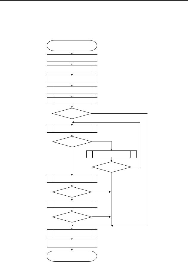
Figure 1-1. Flow of Self Programming (rewriting contents of flash memory)
Starting self programming
<1> FLMD0 pin: Low → High
<2> 
 FlashStart
<3> Setting operating environment
<4> |
FlashEnv |
|
|
<5> |
CheckFLMD |
|
|
|
Normal |
No |
|
|
completion? |
|
|
|
Yes |
|
|
<6> |
FlashBlockBlankCheck |
|
|
|
Erased? |
No |
|
|
|
|
|
|
Yes |
|
|
|
<7> |
FlashBlockErase |
|
|
|
Normal |
Yes |
|
|
completion? |
|
|
|
No |
|
<8> |
FlashWordWrite |
|
|
|
Normal |
No |
|
|
completion? |
|
|
|
Yes |
|
|
<9> |
FlashBlockVerify |
|
|
|
Normal |
No |
|
|
completion? |
|
|
|
Yes |
|
|
<10> |
FlashEnd |
|
|
<11> FLMD0 pin: High → Low
End of self programming
12 |
User’s Manual U17516EJ1V0UM |

CHAPTER 1 GENERAL
<1> |
Preprocessing (setting of hardware environment) |
|
As preprocessing, make the FLMD0 pin high (refer to 2.1 Hardware Environment). |
<2> |
Preprocessing (declaring start of self programming) |
|
As preprocessing, call the self programming start library FlashStart to declare the start of self programming. |
<3> |
Preprocessing (setting of software environment) |
|
As preprocessing, save register bank 3 and specify a work area (refer to 2.2 Software Environment). |
<4> |
Preprocessing (initializing entry RAM) |
|
As preprocessing, call the initialize library FlashEnv to initialize the entry RAM. |
<5> |
Preprocessing (checking voltage level) |
|
As preprocessing, call the mode check library CheckFLMD and check the voltage level. |
<6> |
Checking erasing of specified block (1 KB) |
|
Call the block blank check library FlashBlockBlankCheck to check if the specified block (1 KB) has been erased. |
<7> |
Erasing specified block (1 KB) |
|
Call the block erase library FlashBlockErase to erase a specified block (1 KB). |
<8> |
Writing data of 1 to 64 words to specified addresses |
|
Call the word write library FlashWordWrite to write data of 1 to 64 words to specified addresses. |
<9> |
Verifying specified block (1 KB) (internal verification) |
|
Call the block verify library FlashBlockVerify to verify a specified block (1 KB) (internal verification). |
<10> Post-processing (declaring end of self programming)
As post-processing, call the self programming end library FlashEnd to declare the end of self programming.
<11> Post-processing (setting of hardware environment)
As post-processing, return the level of the FLMD0 pin to the low level.
User’s Manual U17516EJ1V0UM |
13 |

CHAPTER 1 GENERAL
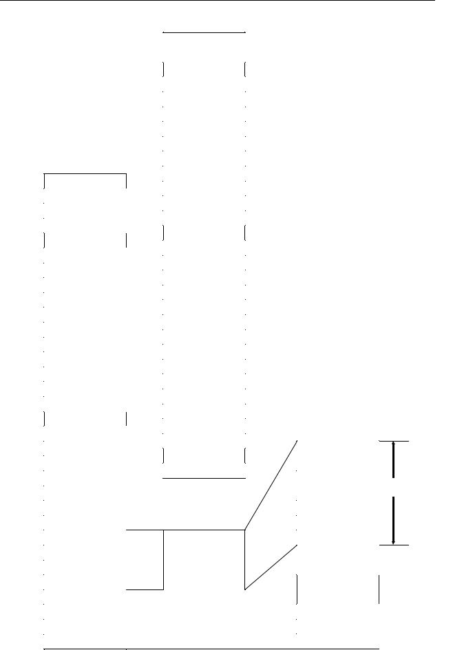
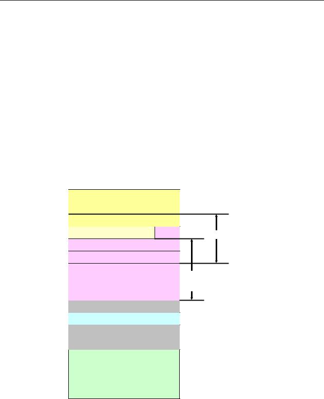
1.3 Bank Number and Block Number
Products in the 78K0/Kx2 Series having flash memory of up to 60 KB have their flash memory divided into 1 KB blocks. Erasing, blank checking, and verification (internal verification) for self programming are performed in these block units. To call the self programming sample library, a block number is specified.
Addresses 0000H to 0FFFH and 1000H to 1FFFH of the 78K0/Kx2 are allocated for boot clusters. A boot cluster is an area that is used to prevent the vector table data and basic functions of the program from being destroyed, and to prevent the user program from being unable to start due to a power failure or because the device was reset while an area including a vector area was being rewritten. For details on the boot cluster, refer to CHAPTER 4 BOOT SWAP FUNCTION.
Figure 1-2 shows the block numbers and boot clusters of a flash memory of up to 60 KB.
78K0/Kx2 products having flash memory of more than 96 KB have banks in an area that is larger than 32 KB. For these products, not only a block number but also a bank number must be specified to call the self programming sample library when performing erasing, blank checking, or verification (internal verification) in the area that is larger than 32 KB during self programming.
Figure 1-3 shows the block numbers and boot clusters of a flash memory of more than 96 KB.
14 |
User’s Manual U17516EJ1V0UM |
CHAPTER 1 GENERAL
Figure 1-2. Block Numbers and Boot Clusters (flash memory of up to 60 KB)
8000H
7C00H
7800H
7400H
7000H
6C00H
6800H
6400H
6000H
5C00H
5800H
5400H
5000H
4C00H
4800H
4400H
4000H
3C00H
3800H
3400H
3000H
2C00H
2800H
2400H
2000H
1C00H
1800H
1400H
1000H
0C00H
0800H
0400H
0000H
Block 31
Block 30
Block 29
Block 28
Block 27
Block 26
Block 25
Block 24
Block 23
Block 22
Block 21
Block 20
Block 19
Block 18
Block 17
Block 16
Block 15
Block 14
Block 13
Block 12
Block 11
Block 10
Block 9
Block 8
Block 7
Block 6
Block 5
Block 4
Block 3
Block 2
Block 1
Block 0
F800H
F000H
EC00H
E800H
E400H
E000H
DC00H
D800H
D400H
D000H
CC00H
C800H
C400H
C000H
BC00H
B800H
B400H
B000H
AC00H
A800H
A400H
A000H
9C00H
9800H
9400H
9000H
8C00H
8800H
8400H
8000H
2000H
1FFFH
0FFFH
0000H
Internal expansion RAM
Block 59
Block 58
Block 57
Block 56
Block 55
Block 54
Block 53
Block 52
Block 51
Block 50
Block 49
Block 48
Block 47
Block 46
Block 45
Block 44
Block 43
Block 42
Block 41
Block 40
Block 39
Block 38
Block 37
Block 36
Block 35
Block 34 |
1FFFH |
CALLF entry |
|
|
|
|
|
||
Block 33 |
|
|
||
|
2048 bytes |
|
||
|
|
|
|
|
Block 32 |
17FFH |
Program area |
|
|
|
|
|
||
|
|
|
Area subject to boot |
|
|
|
|
|
|
|
|
1081H |
1919 bytes |
swapping |
|
|
|
|
|
|
|
1080H |
Option byte |
|
|
|
|
|
|
|
|
107FH |
CALLT table 64 bytes |
|
|
|
|
|
|
|
|
|
Vector table 64 bytes |
|
|
|
0FFFH |
CALLF entry |
|
Boot cluster 1 |
|
|
||
|
2048 bytes |
|
||
|
|
0800H |
|
|
|
|
|
|
|
|
|
07FFH |
Program area |
|
|
|
|
|
|
|
|
0081H |
1919 bytes |
|
|
|
|
|
|
Boot cluster 0 |
0080H |
Option byte |
|
|
|
|
|||
007FH |
|
|
||
|
|
CALLT table 64 bytes |
|
|
|
|
|
|
|
|
|
003FH |
Vector table 64 bytes |
|
|
|
0000H |
|
|
User’s Manual |
U17516EJ1V0UM |
|
|
15 |
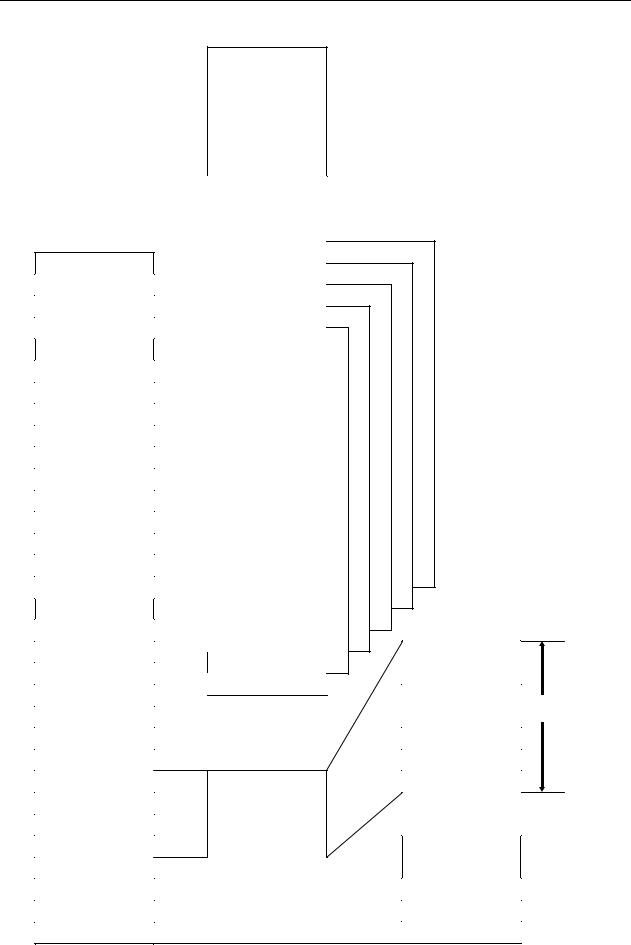
CHAPTER 1 GENERAL
8000H
7C00H
7800H
7400H
7000H
6C00H
6800H
6400H
6000H
5C00H
5800H
5400H
5000H
4C00H
4800H
4400H
4000H
3C00H
3800H
3400H
3000H
2C00H
2800H
2400H
2000H
1C00H
1800H
1400H
1000H
0C00H
0800H
0400H
0000H
Figure 1-3. Block Numbers and Boot Clusters (flash memory of 96 KB or more)
Block 31
Block 30
Block 29
Block 28
Block 27
Block 26
Block 25
Block 24
Block 23
Block 22
Block 21
Block 20
Block 19
Block 18
Block 17
Block 16
Block 15
Block 14
Block 13
Block 12
Block 11
Block 10
Block 9
Block 8
Block 7
Block 6
Block 5
Block 4
Block 3
Block 2
Block 1
Block 0
F800H
E000H DFFFH
C000H
BC00H
B800H
B400H
B000H
AC00H
A800H
A400H
A000H
9C00H
9400H
9000H
8C00H
8800H
8400H
8000H
2000H
1FFFH
0FFFH
0000H
Internal expansion RAM
Use prohibited
Block 47
Block 46
Block 45
Block 44
Block 43
Block 42
Block 41
Block 40
Block 39
Block 38
Block 37
Block 36
Block 35
Block 34
Block 33
Block 32
Bank 0
Boot cluster 1
Boot cluster 0
Bank |
2 Bank |
1FFFH3Bank |
4 Bank |
5 Bank |
|
1 |
|
|
|
CALLF entry |
|
|
|
|
|
2048 bytes |
|
|
|
17FFH |
|
Program area |
|
|
|
|
|
Area subject to boot |
|
|
|
|
|
|
|
|
|
1081H |
|
1919 bytes |
swapping |
|
|
|
|
|
|
|
|
1080H |
|
Option byte |
|
|
|
|
|
|
|
|
|
107FH |
|
CALLT table 64 bytes |
|
|
|
|
|
|
|
|
|
|
|
Vector table 64 bytes |
|
|
|
0FFFH |
|
CALLF entry |
|
|
|
|
|
|
|
|
|
0800H |
|
2048 bytes |
|
|
|
|
|
|
|
|
|
07FFH |
|
Program area |
|
|
|
|
|
|
|
|
|
0081H |
|
1919 bytes |
|
|
|
|
|
|
|
|
|
0080H |
|
Option byte |
|
|
|
|
|
|
|
|
|
007FH |
|
|
|
|
|
003FH |
|
Vector table 64 bytes |
|
|
|
0000H |
|
|
16 |
User’s Manual U17516EJ1V0UM |

CHAPTER 1 GENERAL
1.4 Processing Time and Acknowledging Interrupt
Table 1-1 and Table 1-2 show the processing time of the self programming sample library and whether interrupts can be acknowledged. Table 1-1 shows a case where an internal high-speed oscillator is used for the main system clock and Table 1-2 shows a case where an external system clock is used for the main system clock.
The self programming sample library that can acknowledge interrupts has a function to check if an interrupt is generated while processing of the self programming sample library is under execution, and a function to perform post-processing if an interrupt has been generated.
For details on interrupts, refer to CHAPTER 3 INTERRUPT SERVICING DURING SELF PROGRAMMING.
User’s Manual U17516EJ1V0UM |
17 |

18
Table 1-1. Processing Time and Acknowledging Interrupt (with internal high-speed oscillator)
|
|
|
|
Processing Time (unit: microseconds) |
|
|
|
|
|
|||||||
|
|
|
|
|
|
|
|
|
|
|
|
|
|
|||
|
Library Name |
Outside short direct addressing range |
|
|
|
In short direct addressing range |
Acknowledging |
|
||||||||
|
Normal model |
Static model |
|
Normal model |
|
Static model |
Interrupt |
|
||||||||
|
|
|
|
|
||||||||||||
|
|
|
|
|
|
|
|
|
|
|
|
|
|
|
|
|
|
|
Min |
Max |
Min |
|
Max |
|
Min |
|
Max |
|
Min |
|
Max |
|
|
|
|
|
|
|
|
|
|
|
|
|
|
|
|
|
|
|
|
self programming start library |
|
|
|
4.25 |
|
|
|
|
|
|
|
Not acknowledged |
|
||
|
|
|
|
|
|
|
|
|
|
|
|
|
|
|
||
|
initialize library |
|
977.75 |
|
|
|
|
443.5 |
|
|
|
Not acknowledged |
|
|||
|
|
|
|
|
|
|
|
|
|
|
|
|
|
|||
|
mode check library |
753.875 |
753.125 |
|
219.625 |
|
218.875 |
Not acknowledged |
|
|||||||
|
|
|
|
|
|
|
|
|
|
|
|
|
|
|||
|
block blank check library |
12770.875 |
12765.875 |
|
12236.625 |
|
12231.625 |
Acknowledged |
|
|||||||
U17516EJ1V0UMManualUser’s |
|
|
|
|
|
|
|
|
|
|
|
|
|
|
|
|
block erase library |
36909.5 |
356318 |
36904.5 |
|
356296.25 |
|
36363.25 |
|
355771.75 |
|
36358.25 |
|
355750 |
Acknowledged |
|
|
|
|
|
|
|
|
|
|
|
|
|
|
|
|
|
GENERAL1CHAPTER |
|
word write library |
1214 |
2409 |
1207 |
|
2402 |
|
679.75 |
|
1874.75 |
|
672.75 |
|
1867.75 |
Acknowledged |
||
|
|
|
|
|
|
|
||||||||||
|
|
(1214.375) |
(2409.375) |
(1207.375) |
|
(2402.375) |
|
(680.125) |
|
(1875.125) |
|
(673.125) |
|
(1868.125) |
|
|
|
|
|
|
|
|
|
|
|
|
|
|
|
|
|||
|
block verify library |
25618.875 |
25613.875 |
|
25072.625 |
|
25067.625 |
Acknowledged |
|
|||||||
|
|
|
|
|
|
|
|
|
|
|
|
|
|
|
|
|
|
self programming end library |
|
|
|
4.25 |
|
|
|
|
|
|
|
Not acknowledged |
|
||
|
|
|
|
|
|
|
|
|
|
|
|
|||||
|
get information library |
871.25 |
|
866 |
|
|
337 |
|
331.75 |
Not acknowledged |
|
|||||
|
(option value: 03H) |
(871.375) |
(866.125) |
|
(337.125) |
|
(331.875) |
|
|
|||||||
|
|
|
|
|
|
|
|
|
|
|||||||
|
get information library |
863.375 |
858.125 |
|
329.125 |
|
323.875 |
Not acknowledged |
|
|||||||
|
(option value: 04H) |
(863.5) |
(858.25) |
|
(239.25) |
|
|
(324) |
|
|
||||||
|
|
|
|
|
|
|
|
|
|
|
||||||
|
get information library |
1042.75 |
1037.5 |
|
502.25 |
|
|
497 |
Not acknowledged |
|
||||||
|
(option value: 05H) |
(1043.625) |
(1038.375) |
|
(503.125) |
|
(497.875) |
|
|
|||||||
|
|
|
|
|
|
|
|
|
|
|
|
|
|
|||
|
set information library |
105524.75 |
790809.375 |
105523.75 |
|
790808.375 |
|
104978.5 |
|
541143.125 |
|
104977.5 |
|
541142.125 |
Acknowledged |
|
|
|
|
|
|
|
|
|
|
|
|
|
|
|
|
|
|
|
EEPROM write library |
1496.5 |
2691.5 |
1489.5 |
|
2684.5 |
|
962.25 |
|
2157.25 |
|
955.25 |
|
2150.25 |
Acknowledged |
|
|
|
(1496.875) |
(2691.875) |
(1489.875) |
|
(2684.875) |
|
(962.625) |
|
(2157.625) |
|
(955.625) |
|
(2150.625) |
|
|
|
|
|
|
|
|
|
|
|
|
|
|
|
|
|
|
|
Remark Values in parentheses are when the write start address structure is placed outside of internal high-speed RAM.

Table 1-2. Processing Time and Acknowledging Interrupt (with external system clock used)
|
|
|
|
|
|
|
|
|
Processing Time (unit: microseconds) |
|
|
|
|
|
|
|
|
|
|||||||||||||
|
|
|
|
|
|
|
|
|
|
|
|
|
|
|
|
|
|||||||||||||||
|
Library Name |
Outside short direct addressing range |
|
|
|
|
In short direct addressing range |
|
|
Acknowledging |
|
||||||||||||||||||||
|
Normal model |
|
|
Static model |
Normal model |
|
Static model |
Interrupt |
|
||||||||||||||||||||||
|
|
|
|
|
|
||||||||||||||||||||||||||
|
|
|
|
|
|
|
|
|
|
|
|
|
|
|
|
|
|
|
|
|
|
|
|
|
|
|
|
|
|
|
|
|
|
Min |
|
|
|
Max |
|
|
Min |
|
|
|
|
Max |
Min |
|
|
|
|
|
|
Max |
|
Min |
|
|
|
|
Max |
|
|
|
|
|
|
|
|
|
|
|
|
|
|
|
|
|
|
|
|
|
|
|
|
|
|
|
|
|
|
|
|
|
|
|
self programming start library |
|
|
|
|
|
|
|
|
|
|
|
|
|
Note |
|
|
|
|
|
|
|
|
|
|
|
|
|
|
Not acknowledged |
|
|
|
|
|
|
|
|
|
|
|
|
|
|
34/fX |
|
|
|
|
|
|
|
|
|
|
|
|
|
|
|
|||
|
initialize library |
|
|
|
|
Note |
+ 485.8125 |
|
|
|
|
|
|
|
|
|
|
|
|
Note |
+ 224.6875 |
|
|
|
|
|
Not acknowledged |
|
|||
|
|
|
|
|
49X |
|
|
|
|
|
|
|
|
|
|
|
|
|
49/fX |
|
|
|
|
|
|
||||||
|
mode check library |
Note |
+ 374.75 |
|
|
Note |
+ 374.75 |
Note |
+ 113.625 |
|
Note |
+ 113.625 |
Not acknowledged |
|
|||||||||||||||||
|
35/fX |
|
|
|
29/fX |
|
35/fX |
|
|
29/fX |
|
|
|||||||||||||||||||
|
block blank check library |
Note |
+ 6382.0625 |
|
|
Note |
+ 6382.0625 |
Note |
|
+ 6120.9375 |
|
Note |
|
+ 6120.9375 |
Acknowledged |
|
|||||||||||||||
|
174/fX |
|
|
134/fX |
174/fX |
|
|
134/fX |
|
|
|||||||||||||||||||||
|
block erase library |
Note |
|
|
|
Note |
+ |
|
Note |
|
|
|
|
Note |
Note |
|
|
|
|
|
|
Note |
|
Note |
|
|
|
|
Note |
Acknowledged |
|
|
174/fX |
|
|
|
174/fX |
|
134/fX |
|
|
|
|
134/fX |
174/fX |
|
|
|
|
|
|
174/fX |
|
134/fX |
|
|
|
|
134/fX |
|
|||
|
|
+ 31093.875 |
|
|
298948.125 |
+ 31093.875 |
|
|
+ 298948.125 |
+ 30820.75 |
|
|
|
|
|
+ 298675 |
|
+ 30820.75 |
|
|
|
+ 298675 |
|
|
|||||||
|
|
|
|
|
|
|
|
|
|
|
|
|
|
|
|
|
|
|
|
|
|
|
|
||||||||
|
word write library |
Note |
|
|
|
Note |
Note |
|
|
|
Note |
Note |
|
|
|
|
Note |
Note |
|
|
Note |
Acknowledged |
|
||||||||
|
318(321)/fX |
|
|
318(321)/fX |
|
262(265)/fX |
|
|
|
262(265)/fX |
318(321)/fX |
|
|
|
|
318(321)/fX |
|
262(265)/fX |
|
|
|
262(265)/fX |
|
||||||||
U17516EJ1V0UMManualUser’s |
|
+ 644.125 |
|
|
|
+ 1491.625 |
+ 644.125 |
|
|
|
|
+ 1491.625 |
+ 383 |
|
|
|
|
|
|
+ 1230.5 |
|
+ 383 |
|
|
|
|
+ 1230.5 |
|
|
||
|
|
|
|
|
|
|
|
|
|
|
|
|
|
|
|
|
|
|
|
|
|
|
|
|
|
|
|
|
|
|
|
block verify library |
Note |
+ 13448.5625 |
|
|
Note |
+ 13448.5625 |
Note |
+ 13175.4375 |
|
Note |
+ 13175.4375 |
Acknowledged |
|
||||||||||||||||||
174/fX |
|
|
134/fX |
174/fX |
|
134/fX |
GENERAL1CHAPTER |
||||||||||||||||||||||||
self programming end library |
|
|
|
|
|
|
|
|
|
|
|
|
34X |
Note |
|
|
|
|
|
|
|
|
|
|
|
|
|
|
Not acknowledged |
||
|
|
|
|
|
|
|
|
|
|
|
|
|
|
|
|
|
|
|
|
|
|
|
|
|
|
|
|
|
|||
|
|
|
|
|
|
|
|
|
|
|
|
|
|
|
|
|
|
|
|
|
|
|
|
|
|||||||
|
get information library |
|
Note |
+ 432.4375 |
|
|
Note |
|
+ 432.4375 |
|
|
Note |
|
+ 171.3125 |
|
|
|
Note |
+ 171.3125 |
Not acknowledged |
|
||||||||||
|
171(172)/fX |
|
|
|
129(130)/fX |
|
|
|
171(172)/fX |
|
|
|
|
129(130)/fX |
|
||||||||||||||||
|
(option value: 03H) |
|
|
|
|
|
|
|
|
|
|
|
|
|
|
|
|
|
|
|
|
|
|
|
|
|
|
|
|
|
|
|
|
|
|
|
|
|
|
|
|
|
|
|
|
|
|
|
|
|
|
|
|
|
|||||||||
|
get information library |
|
Note |
+ 427.875 |
|
139(140)/fX |
Note |
+ 427.875 |
181(182)/fX |
Note |
+ 166.75 |
|
|
|
Note |
+ 166.75 |
Not acknowledged |
|
|||||||||||||
|
181(182)/fX |
|
|
|
|
|
|
|
|
|
|
|
139(140)/fX |
|
|
||||||||||||||||
|
(option value: 04H) |
|
|
|
|
|
|
|
|
|
|
|
|
|
|
|
|
|
|
|
|
|
|
|
|
|
|
|
|
|
|
|
|
|
|
|
|
|
|
|
|
|
|
|
|
|
|
|
|
|
|
|
|
|
|||||||||
|
get information library |
|
Note |
+ 496.125 |
|
362(369)/fX |
Note |
+ 496.125 |
|
|
Note |
|
+ 231.875 |
|
|
|
Note |
+ 231.875 |
Not acknowledged |
|
|||||||||||
|
404(411)/fX |
|
|
|
|
|
|
404(411)/fX |
|
|
|
|
|
362(369)/fX |
|
|
|||||||||||||||
|
(option value: 05H) |
|
|
|
|
|
|
|
|
|
|
|
|
|
|
|
|
|
|
|
|
|
|
|
|
|
|
|
|
|
|
|
|
|
|
|
|
|
|
|
|
|
|
|
|
|
|
|
|
|
|
|
|
|
|
|
|
|
|
|
|
|
|
|
set information library |
Note |
|
|
|
Note |
|
|
Note |
|
|
|
|
Note |
Note |
|
|
|
|
|
|
Note |
|
Note |
|
|
|
|
Note |
Acknowledged |
|
|
75/fX |
|
|
|
75/fX |
|
|
67/fX |
|
|
|
|
67/fX |
75/fX |
|
|
|
|
|
|
75/fX |
|
67/fX |
|
|
|
|
67/fX |
|
||
|
|
+ 79157.6875 |
|
|
+ 652400 |
|
+ 79157.6875 |
|
|
|
+ 652400 |
+ 78884.5625 |
|
|
+ 527566.875 |
+ 78884.5625 |
|
+ 527566.875 |
|
|
|||||||||||
|
|
|
|
|
|
|
|
|
|
|
|
|
|
|
|
|
|
|
|
|
|
|
|
||||||||
|
EEPROM write library |
Note |
|
|
|
Note |
Note |
|
|
|
Note |
Note |
|
|
|
|
Note |
Note |
|
|
Note |
Acknowledged |
|
||||||||
|
318(321)/fX |
|
|
318(321)/fX |
|
262(265)/fX |
|
|
|
262(265)/fX |
318(321)/fX |
|
|
|
|
318(321)/fX |
|
262(265)/fX |
|
|
|
262(265)/fX |
|
||||||||
|
|
+ 799.875 |
|
|
|
+ 1647.375 |
+ 799.875 |
|
|
|
|
+ 1647.375 |
+ 538.75 |
|
|
|
|
|
|
+ 1386.25 |
|
+ 538.75 |
|
|
|
|
+ 1386.25 |
|
|
||
|
|
|
|
|
|
|
|
|
|
|
|
|
|
|
|
|
|
|
|
|
|
|
|
|
|
|
|
|
|
|
|
Note fX: Operating frequency of external system clock
Remark Values in parentheses are when the write start address structure is placed outside of internal high-speed RAM.
19
CHAPTER 2 PROGRAMMING ENVIRONMENT
This chapter explains the hardware environment and software environment necessary for the user to rewrite flash memory by using the self programming sample library.
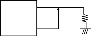
2.1 Hardware Environment
To execute self programming, a circuit that controls the voltage on the FLMD0 pin of the 78K0/Kx2 is necessary. The voltage on the FLMD0 pin must be low while an ordinary user program is being executed (in normal operation
mode) and high while self programming is being executed (in flash rewriting mode).
While the FLMD0 pin is low, the firmware and software for rewriting run, but the circuit for rewriting flash memory does not operate. Therefore, the flash memory is not actually rewritten.
A self programming sample library that makes the FLMD0 pin high is not provided. Therefore, to rewrite the flash memory, the voltage level of the FLMD0 pin must be made high by manipulating a port through user program, before calling the self programming start library.
Here is an example of the circuit that changes the voltage on the FLMD0 pin by manipulating a port.
Figure 2-1. FLMD0 Voltage Generator
FLMD0
78K0/Kx2 |
10 kΩ (recommended) |
Output port
20 |
User’s Manual U17516EJ1V0UM |
CHAPTER 2 PROGRAMMING ENVIRONMENT
2.2 Software Environment
The self programming sample library allocates its program to a user area and consumes about 500 bytes of the program area. The self programming sample library itself uses the CPU (register bank 3), work area (entry RAM), stack, and data buffer.
The following table lists the necessary software resources.
Table 2-1. Software Resources
Item |
Description |
Restriction |
|
|
|
CPU |
Register bank 3 |
− |
|
|
|
Work area |
Entry RAM: 100 bytes |
Internal high-speed RAM outside short addressing range or |
|
|
internal high-speed RAM in short direct addressing range with |
|
|
first address as FE20H (Refer to 2.2.1 Entry RAM.) |
|
|
|
Stack |
39 bytes max. |
Internal high-speed RAM other than FE20H to FE83H (Refer to |
|
Remark Use the same stack as for the |
2.2.2 Stack and data buffer.) |
|
user program. |
|
|
|
|
Data buffer |
1 to 256 bytes |
Internal high-speed RAM other than FE20H to FE83H (Refer to |
|
Remark The size of this buffer varies |
2.2.2 Stack and data buffer.) |
|
depending on the writing unit |
|
|
specified by the user program. |
|
|
|
|
Program area |
Normal model: 525 bytes |
Within 0000H to 7FFFH (32 KB) |
|
Static model: 432 bytes |
Caution The self programming sample library and the |
|
Remark Supplied as an |
user program that calls the self programming |
|
assembly-language source. |
sample library must always be located within the |
|
|
above range, because the firmware built into the |
|
|
product is allocated to addresses starting from |
|
|
8000H. |
|
|
|
Cautions 1. The self programming operation is not guaranteed if the user manipulates the above resources. Do not manipulate these resources during a self programming operation.
2.The user must release the above resources used by the self programming sample library before calling the self programming sample library.
User’s Manual U17516EJ1V0UM |
21 |
CHAPTER 2 PROGRAMMING ENVIRONMENT
2.2.1Entry RAM
The self programming sample library uses a work area of 100 bytes. This area is called entry RAM.
As the entry RAM, 100 bytes are automatically allocated, starting from the first address that is specified when the initialize library is called. Therefore, the first address of the entry RAM can be specified in the range from FB00H to FE20H.
In addition, a data buffer used by the initialize library to actually write data to the flash memory must be allocated to an area that is within the range from 1 to 256 bytes and is other than the work area. For details on the data buffer, refer to 2.2.2 Stack and data buffer.
The range in which the entry RAM can be allocated is shown below.
Figure 2-2. Allocation Range of Entry RAM
FFFFH |
Special function registers (SFRs) |
|
|
|
|
|
|
|
|
|
|
||
|
256 bytes |
|
|
|
|
|
FF20H |
|
|
|
|
|
|
FF00H |
|
|
|
|
|
|
FEFFH |
General-purpose registers |
|
|
|
Short direct addressing |
|
|
32 bytes |
|
|
|
|
|
|
|
|
|
|
|
|
FE83H |
|
|
|
|
|
|
FE20H |
|
|
|
|
|
|
|
Internal high-speed RAM |
|
|
|
|
|
|
1024 bytes |
|
Entry RAM allocation range |
|||
|
|
|
|
|
||
FB00H |
|
|
|
|
|
|
FAFFH |
Use prohibited |
|
|
|
|
|
FA20H |
|
|
|
|
||
|
|
|
|
|
|
|
FA00H |
Buffer RAM 32 bytes |
|
|
|
|
|
|
|
|
|
|
|
|
F9FFH |
Use prohibited |
|
|
|
|
|
|
|
|
|
|
||
F800H |
|
|
|
|
|
|
F7FFH |
Internal expansion high-speed RAM |
|
|
|
|
|
|
|
|
|
|
||
|
1024 bytes |
|
|
|
|
|
|
|
|
|
|
|
|
Caution The size of the internal expansion high-speed RAM varies depending on the product.
For the size of the internal expansion high-speed RAM, refer to the user’s manual of each product.
22 |
User’s Manual U17516EJ1V0UM |
CHAPTER 2 PROGRAMMING ENVIRONMENT
2.2.2Stack and data buffer
The self programming sample library writes data to flash memory by using the CPU. Therefore, a self programming operation is performed by using the stack specified by the user program.
The stack must be allocated by stack processing of the self programming operation so that the entry RAM and the RAM used by the user are not cleared. Therefore, the stack can be allocated in the internal high-speed RAM at addresses other than FE20H to FE83H.
A data buffer is automatically allocated from the first address and by the number of data specified when the word write library is called. Therefore, the first address of the data buffer can be specified in the internal high-speed RAM at an address other than FE20H to FE83H, just as for the stack pointer.
Note that data to be written to the flash memory must be appropriately set and processed before the word write library is called.
The following figure shows the range in which the stack pointer and data buffer can be allocated.
Figure 2-3. Allocatable Range for Stack Pointer and Data Buffer
FFFFH
Special function registers (SFRs) 256 bytes
FF20H
FF00H
FEFFH General-purpose registers 32 bytes
FE83H |
Use prohibited |
FE20H |
|
Internal high-speed RAM 1024 bytes
FB00H
FAFFH Use prohibited
FA20H
Buffer RAM 32 bytes
FA00H
F9FFH
Use prohibited
F800H
F7FFH
Internal expansion high-speed RAM 1024 bytes
Short direct addressing
Range where stack and data buffer can be allocated (except FE20H to FE83H)
Caution The size of the internal expansion high-speed RAM varies depending on the product.
For the size of the internal expansion high-speed RAM, refer to the user’s manual of each product.
User’s Manual U17516EJ1V0UM |
23 |
CHAPTER 3 INTERRUPT SERVICING DURING SELF
PROGRAMMING
3.1 Overview
An interrupt can be generated, even while self programming is executed, in some self programming sample libraries of the 78K0/Kx2.
However, unlike the case for an ordinary interrupt, the user must decide whether the processing that has been interrupted should be resumed, by checking the return value from the self programming sample library.
24 |
User’s Manual U17516EJ1V0UM |

CHAPTER 3 INTERRUPT SERVICING DURING SELF PROGRAMMING
The following figure illustrates the flow of processing if an interrupt is generated while processing of the self
programming sample library is being executed.
Figure 3-1. Flow of Processing in Case of Interrupt
Interrupt handler
Servicing starts.
Servicing ends.
User program |
Library |
Self programming starts. |
|
|
|
FLMD0 pin: Low → High |
|
|
|
Interrupt
occurs.
FlashStart
Setting of operating environment
1
Servicing starts.
DI
Calling library
EI
Processing is stopped.
Stopped (= 1FH)
Return value
Yes
Retry? 1
No
EndFlashEnd
FLMD0 pin: High → Low
End of self programming
User’s Manual U17516EJ1V0UM |
25 |

CHAPTER 3 INTERRUPT SERVICING DURING SELF PROGRAMMING
The following table shows how the processing of the self programming sample libraries that acknowledge interrupts is resumed after the processing has been stopped by the occurrence of an interrupt.
|
Table 3-1. Resume Processing Stopped by Interrupt |
|
|
|
|
Library Name |
|
Resuming Method |
|
|
|
block blank check library |
|
Call the block blank check library FlashBlockBlankCheck to resume processing to check |
|
|
block erasure that has been stopped by the occurrence of an interrupt. |
|
|
|
block erase library |
|
To resume processing to erase blocks that was stopped by the occurrence of an |
|
|
interrupt, call the block blank check library FlashBlockBlankCheck and check whether |
|
|
blocks that should be erased have been erased. Then, call the block erase library |
|
|
FlashBlockErase. |
|
|
|
word write library |
|
Call the word write library FlashWordWrite to resume data write processing that was |
|
|
stopped by the occurrence of an interrupt. |
|
|
|
block verify library |
|
Call the block verify library FlashBlockVerify to resume block verify processing that was |
|
|
stopped by the occurrence of an interrupt. |
|
|
|
set information library |
|
Call the set information library FlashSetInfo to resume flash information setting |
|
|
processing that was stopped by the occurrence of an interrupt. |
|
|
|
EEPROM write library |
|
Call the EEPROM write library FlashEEPROMWrite to resume processing to write data |
|
|
during EEPROM emulation that was stopped by the occurrence of an interrupt. |
|
|
|
Remark An interrupt is not acknowledged until all of the processing of the above self programming sample libraries has been completed, because these libraries execute their processing with interrupts disabled.
26 |
User’s Manual U17516EJ1V0UM |

CHAPTER 3 INTERRUPT SERVICING DURING SELF PROGRAMMING
3.2 Interrupt Response Time
Unlike the case for an ordinary interrupt, generation of an interrupt during execution of self programming is accomplished via post-interrupt servicing in the self programming sample library (such as setting 0x1F as the return value from the self programming sample library). Consequently, the response time is longer than that for an ordinary interrupt.
When an interrupt occurs during self programming execution, both the interrupt response time of the self programming sample library, as well as the interrupt response time of the device used, are necessary.
Remark For the response time of each device, refer to the user’s manual of each device.
Table 3-2 and Table 3-3 show the interrupt response time of the self programming sample library. Table 3-2 is a case where the internal high-speed oscillator is used to generate the main system clock, and Table 3-3 is a case where an external system clock is used as the main system clock.
Table 3-2. |
Interrupt Response Time (with Internal High-Speed Oscillator) |
|
|||||
|
|
|
|
|
|
|
|
|
|
|
Interrupt Response Time (Unit: Microseconds) |
|
|||
|
|
|
|
|
|
||
Library Name |
|
Entry RAM outside short direct addressing |
Entry RAM inside short direct addressing |
||||
|
|
range |
range (from FE20H) |
||||
|
|
|
|||||
|
|
|
|
|
|
|
|
|
|
Min |
|
Max |
Min |
|
Max |
|
|
|
|
|
|
|
|
block blank check library |
|
391.25 |
|
1300.5 |
81.25 |
|
727.5 |
|
|
|
|
|
|
|
|
block erase library |
|
389.25 |
|
1393.5 |
79.25 |
|
820.5 |
|
|
|
|
|
|
|
|
word write library |
|
394.75 |
|
1289.5 |
84.75 |
|
716.5 |
|
|
|
|
|
|
|
|
block verify library |
|
390.25 |
|
1324.5 |
80.25 |
|
751.5 |
|
|
|
|
|
|
|
|
set information library |
|
387 |
|
852.5 |
77 |
|
279.5 |
|
|
|
|
|
|
|
|
EEPROM write library |
|
399.75 |
|
1395.5 |
89.75 |
|
822.5 |
|
|
|
|
|
|
|
|
Remark An interrupt is not acknowledged until all of the processing of the above self programming sample libraries has been completed, because these libraries execute their processing with interrupts disabled.
User’s Manual U17516EJ1V0UM |
27 |

CHAPTER 3 INTERRUPT SERVICING DURING SELF PROGRAMMING
Table 3-3. Interrupt Response Time (with External System Clock)
|
|
Interrupt Response Time (Unit: Microseconds) |
|
|||
|
|
|
|
|
||
Library Name |
Entry RAM outside short direct addressing |
Entry RAM inside short direct addressing |
||||
|
range |
range (from FE20H) |
||||
|
|
|||||
|
|
|
|
|
|
|
|
Min |
|
Max |
Min |
|
Max |
|
|
|
|
|
|
|
block blank check library |
18/fxNote + 192 |
|
28/fxNote + 698 |
18/fxNote + 55 |
|
28/fxNote + 462 |
|
|
|
|
|
|
|
block erase library |
18/fxNote + 186 |
|
28/fxNote + 745 |
18/fxNote + 49 |
|
28/fxNote + 509 |
|
|
|
|
|
|
|
word write library |
22/fxNote + 189 |
|
28/fxNote + 693 |
22/fxNote + 52 |
|
28/fxNote + 457 |
|
|
|
|
|
|
|
block verify library |
18/fxNote + 192 |
|
28/fxNote + 709 |
18/fxNote + 55 |
|
28/fxNote + 473 |
|
|
|
|
|
|
|
set information library |
16/fxNote + 190 |
|
28/fxNote + 454 |
16/fxNote + 53 |
|
28/fxNote + 218 |
|
|
|
|
|
|
|
EEPROM write library |
22/fxNote + 191 |
|
28/fxNote + 783 |
22/fxNote + 54 |
|
28/fxNote + 547 |
|
|
|
|
|
|
|
Note fX: Operating frequency of external system clock
Remark An interrupt is not acknowledged until all of the processing of the above self programming sample libraries has been completed, because these libraries execute their processing with interrupts disabled.
28 |
User’s Manual U17516EJ1V0UM |

CHAPTER 3 INTERRUPT SERVICING DURING SELF PROGRAMMING
3.3 Description Example
This section shows an example of writing a user program that resumes erase processing that was stopped by the occurrence of an interrupt during execution of a self programming sample library (block erase library).
User’s Manual U17516EJ1V0UM |
29 |

CHAPTER 3 INTERRUPT SERVICING DURING SELF PROGRAMMING
ERS_RTRY: |
|
|
|
; Main processing |
|
|
|
MOV |
A, #0 |
; Sets 0 as the bank number of the block to be erased. |
|
MOV |
B, #10 |
; Sets 10 as the block number of the block to be erased. |
|
DI |
|
; |
Disables interrupts. |
CALL |
!_FlashBlockErase |
; |
Calls the block erase library. |
EI |
|
; |
Enables interrupts. |
CMP |
A, #1FH |
; |
Checks whether a stop status is set. |
BZ |
$BLN_RTRY |
; |
If the stop status is set, |
|
|
; |
jumps to resume processing BLN_RTRY. |
CMP |
A, #00H |
; Checks whether execution has been correctly |
|
|
|
|
completed. |
BNZ |
$ERS_FALSE_END |
; |
Jumps to abnormal termination ERS_FALSE_END if |
BR |
ERS_TRUE_END |
|
execution has not been correctly completed. |
|
|
||
BLN_RTRY: |
|
|
|
; Resume processing |
|
|
|
MOV |
A, #0 |
; |
Sets 0 as the bank number of the block to be |
|
|
|
blank-checked. |
MOV |
B, #10 |
; Sets 10 as the block number of the block to be |
|
|
|
|
blank-checked. |
DI |
|
; |
Disables interrupts. |
|
|
; |
Calls the block blank check library. |
CALL !_FlashBlockBlankCheck |
|
||
EI |
|
; |
Enables interrupts. |
CMP |
A, #1FH |
; |
Checks whether a stop status is set. |
BZ |
$BLN_RTRY |
; |
If the stop status is set, |
|
|
; |
retries the resume processing. |
CMP |
A, #00H |
; Checks whether execution has been correctly |
|
|
|
|
completed. |
BNZ |
$ERS_RTRY |
; Retries the main processing if execution has not been |
|
|
|
|
correctly completed. |
; Clears the internal status of the stop processing |
|||
MOVW |
AX, #EntryRAM |
; Sets the first address of entry RAM. |
|
CALL |
!_FlashEnv |
; Calls the initialize library. |
|
ERS_TRUE_END:
; Normal completion
ERS_FALSE_END:
; Abnormal termination
Caution It is assumed that the entry RAM has already been set.
30 |
User’s Manual U17516EJ1V0UM |
Loading...