


DATA SHEET
PHOTOCOUPLER
PS9701
HIGH SPEED DIGITAL OUTPUT TYPE 5-PIN SOP PHOTOCOUPLER
−NEPOCTM Series−
DESCRIPTION
The PS9701 is an optically coupled isolator containing a GaAlAs LED on light emitting side (input side) and a photodiode and a signal processing circuit on light receiving side (output side) on one chip.
This is SOP (Small Outline Package) type for high-density applications.
FEATURES
•High isolation voltage (BV = 2 500 Vr.m.s.)
•Small and thin package (5-pin SOP)
• High-speed response (tPHL = 36 ns TYP., tPLH = 60 ns TYP.)
• Low threshold input current (IFHL = 2.5 mA TYP.)
• Open-collector type
•Ordering number of taping product: PS9701-1-E3, E4, F3, F4
•UL approved: File No. E72422 (S)
•VDE0884 approved (Option)
APPLICATIONS
•Computer and peripheral manufactures
•Measurement equipment
•Audio-Visual
The information in this document is subject to change without notice. Before using this document, please confirm that this is the latest version.
Not all devices/types available in every country. Please check with local NEC representative for availability and additional information.
Document No. P11437EJ4V0DS00 (4th edition) |
The mark • shows major revised points. |
|
|
Date Published September 1999 NS CP(K) |
© |
|
1994, 1999 |
Printed in Japan |
|
||
|
|||
|

PS9701
2.1±0.2 |
2.0 |
|
0.1±0.1 |
PACKAGE DIMENSIONS in millimeters
4.0±0.5
|
TOP VIEW |
||
6 |
5 |
4 |
|
|
|
1. |
Anode |
|
|
3. |
Cathode |
|
|
4. GND |
|
|
|
5. |
VO |
|
|
6. |
VCC |
1 |
|
3 |
|
|
|
7.0±0.3 |
|
|
|
4.4 |
|
+0.10 –0.05 |
|
|
|
0.15 |
|
|
|
1.27 |
0.5±0.3 |
0.4–0+0..0510 |
0.25 M |
2 |
Data Sheet P11437EJ4V0DS00 |

PS9701
ORDERING INFORMATION
Part Number |
Package |
Packing Style |
Safety Standards |
Application Part |
Approval |
Number*1 |
|||
|
|
|
|
|
PS9701 |
5-pin SOP |
Magazine case 100 pcs |
UL approved |
PS9701 |
|
|
|
|
|
PS9701-E3 |
|
Embossed Tape 900 pcs/reel |
|
|
|
|
|
|
|
PS9701-E4 |
|
|
|
|
|
|
|
|
|
PS9701-F3 |
|
Embossed Tape 3 500 pcs/reel |
|
|
|
|
|
|
|
PS9701-F4 |
|
|
|
|
|
|
|
|
|
PS9701-V |
|
Magazine case 100 pcs |
VDE0884 approved |
|
|
|
|
|
|
PS9701-V-E3 |
|
Embossed Tape 900 pcs/reel |
|
|
|
|
|
|
|
PS9701-V-E4 |
|
|
|
|
|
|
|
|
|
PS9701-V-F3 |
|
Embossed Tape 3 500 pcs/reel |
|
|
|
|
|
|
|
PS9701-V-F4 |
|
|
|
|
|
|
|
|
|
*1 For the application of the Safety Standard, following part number should be used.
ABSOLUTE MAXIMUM RATINGS (TA = 25 °C, unless otherwise specified)
|
Parameter |
Symbol |
Ratings |
Unit |
|
|
|
|
|
Diode |
Forward Current |
IF |
30 |
mA |
|
|
|
|
|
|
Reverse Voltage |
VR |
5 |
V |
|
|
|
|
|
Detector |
Supply Voltage |
VCC |
7 |
V |
|
|
|
|
|
|
Output Voltage |
VO |
7 |
V |
|
|
|
|
|
|
Output Current |
IO |
50 |
mA |
|
|
|
|
|
|
Power Dissipation |
PC |
85 |
mW |
|
|
|
|
|
Isolation Voltage*1 |
BV |
2 500 |
Vr.m.s. |
|
|
|
|
|
|
Operating Ambient Temperature |
TA |
–40 to +85 |
°C |
|
|
|
|
|
|
Storage Temperature |
Tstg |
–55 to +125 |
°C |
|
|
|
|
|
|
*1 AC voltage for 1 minute at TA = 25 °C, RH = 60 % between input and output
RECOMMENDED OPERATING CONDITIONS
Parameter |
Symbol |
MIN. |
TYP. |
MAX. |
Unit |
|
|
|
|
|
|
Low Level Input Current |
IFL |
0 |
|
250 |
μA |
|
|
|
|
|
|
High Level Input Current |
IFH |
5 |
7.5 |
15 |
mA |
|
|
|
|
|
|
Supply Voltage |
VCC |
4.5 |
5.0 |
5.5 |
V |
|
|
|
|
|
|
Operating Ambient Temperature |
TA |
0 |
25 |
70 |
°C |
|
|
|
|
|
|
Remark By-pass capacitor of more than 0.1 μF is used between VCC and GND near the device.
Data Sheet P11437EJ4V0DS00 |
3 |
PS9701
ELECTRICAL CHARACTERISTICS (TA = 0 to +70 °C, unless otherwise specified)
|
Parameter |
Symbol |
Conditions |
MIN. |
TYP. |
MAX. |
Unit |
|
|
|
|
|
|
|
|
|
|
Diode |
Forward Voltage |
VF |
IF = 10 mA, TA = 25 °C |
1.4 |
1.65 |
1.9 |
V |
|
|
|
|
|
|
|
|
|
|
|
Reverse Current |
IR |
VR = 5 V, TA = 25 °C |
|
|
10 |
μA |
|
|
|
|
|
|
|
|
|
|
|
Terminal Capacitance |
Ct |
V = 0 V, f = 1 MHz, TA = 25 °C |
|
60 |
|
pF |
|
|
|
|
|
|
|
|
|
|
Detector |
High Level Output Current |
IOH |
VCC = VO = 5.5 V, IF = 250 μA |
|
2 |
250 |
μA |
|
|
|
|
|
|
|
|
|
|
|
Low Level Output Voltage |
VOL |
VCC = 5.5 V, IF = 7.5 mA, IO = 13 mA |
|
0.3 |
0.6 |
V |
|
|
|
|
|
|
|
|
|
|
|
High Level Supply Current |
ICCH |
VCC = 5.5 V, IF = 0 mA |
4 |
6 |
8 |
mA |
|
|
|
|
|
|
|
|
|
|
|
Low Level Supply Current |
ICCL |
VCC = 5.5 V, IF = 10 mA |
9 |
12 |
15 |
mA |
|
|
|
|
|
|
|
|
|
|
Coupled |
Threshold Input Current |
IFHL |
|
TA = 25 °C |
0.5 |
2.5 |
5.0 |
mA |
|
(H → L) |
|
|
|
|
|
|
|
|
|
VCC = 5 V, VO = 0.8 V, RL = 350 Ω |
|
|
7 |
|
||
|
|
|
|
|
|
|||
|
|
|
|
|
|
|
|
|
|
Isolation Resistance |
RI-O |
VI-O = 1 kVDC, RH = 40 to 60 %, |
1011 |
|
|
Ω |
|
|
|
|
TA = 25 °C |
|
|
|
|
|
|
|
|
|
|
|
|
|
|
|
Isolation Capacitance |
CI-O |
V = 0 V, f = 1 MHz, TA = 25 °C |
|
0.6 |
|
pF |
|
|
|
|
|
|
|
|
|
|
|
Propagation Delay Time |
tPHL |
VCC = 5 V, IF = 7.5 mA, RL = 350 Ω, |
|
36 |
75 |
ns |
|
|
(H → L) *1 |
|
CL = 15 pF, TA = 25 °C |
|
|
|
|
|
|
|
|
|
|
|
|
|
|
|
Propagation Delay Time |
tPLH |
|
|
|
60 |
75 |
|
|
(L → H) *1 |
|
|
|
|
|
|
|
|
|
|
|
|
|
|
|
|
|
Rise Time |
tr |
|
|
|
20 |
|
|
|
|
|
|
|
|
|
|
|
|
Fall Time |
tf |
|
|
|
10 |
|
|
|
|
|
|
|
|
|
|
|
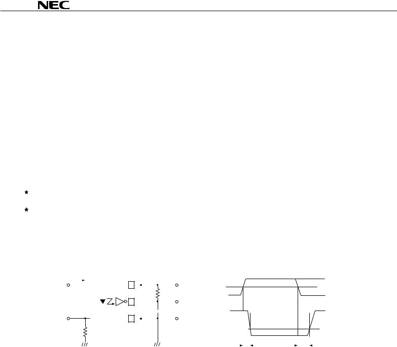
*1 Test circuit for propagation delay time
|
|
IF |
|
|
|
|
|
|
|
|
|
|
|
|
|
|
|
|
|
|
|
|
|
|
|
|
|
|
|
350 mV |
|||
|
|
|
|
|
|
|
|
|
|
|
|
|
|
|
|
|
|
|
Input |
|
|
|
|
|
(IF = 7.5 mA) |
||||||||
Pulse Input |
|
|
|
|
|
1 |
|
|
|
|
|
6 |
|
|
|
|
|
|
|
|
|
VCC = 5 V |
|
|
|
|
|
175 mV |
|||||
(PW = 1 μs |
|
|
|
|
|
|
|
|
|
|
0.1 |
|
|
|
RL |
= 350 Ω |
|
|
|
|
|
|
|
|
|
|
(IF = 3.75 mA) |
||||||
|
|
|
|
|
|
|
|
|
|
|
|
|
|
|
|
|
|||||||||||||||||
|
|
|
|
|
|
|
|
|
|
μF |
|
|
0 |
|
|
|
|
|
|
|
|
|
|
||||||||||
Duty Cycle = 1/10) |
|
|
|
|
|
|
|
|
|
|
|
|
|
|
|
|
|
|
|
|
|
|
|
|
|
||||||||
|
|
|
|
|
|
5 |
|
|
|
|
|
|
|
|
|
VO |
5 V |
|
|
|
|
|
|
|
|
|
|||||||
|
|
|
|
|
|
|
|
|
|
|
|
|
|
|
|
|
|
|
CL |
|
|
|
|
|
|
|
|
|
|
||||
|
|
|
|
|
|
|
|
|
|
|
|
|
|
|
|
|
|
|
|
|
|
|
|
|
|
|
|
|
|
|
|||
|
|
|
|
|
|
|
|
|
|
|
|
|
|
|
|
|
|
|
|
|
|
|
|
|
|
|
|||||||
|
|
|
|
|
|
|
|
|
|
|
|
|
|
|
|
|
|
|
|
|
|
|
|
|
|
|
|
|
|||||
|
|
|
|
|
|
|
|
|
|
|
|
|
|
|
|
|
|
|
|
|
|
|
|
|
|
|
|||||||
IF Monitor |
3 |
|
|
|
|
|
4 |
|
|
|
|
|
|
|
|
|
|
Output |
|
|
|
|
|
|
|
|
1.5 V |
||||||
|
|
|
|
|
|
|
|
|
|
|
|
|
|
|
|
|
|
|
|
|
|
|
|||||||||||
51 Ω |
|
|
|
|
|
|
|
|
|
|
|
|
|
|
|
|
|
|
|
|
|
|
|
|
|
|
|
||||||
|
|
|
|
|
|
|
|
|
|
|
|
|
|
|
|
|
|
|
|
|
|
|
|
|
|
|
|||||||
|
|
|
|
|
|
|
|
|
|
|
|
|
|
|
|
|
|
|
|
|
|
|
|
|
|||||||||
|
|
|
|
|
|
|
|
|
|
|
|
|
|
|
|
|
|
|
|
|
|
|
|
|
|
|
|
|
|
|
|
|
VOL |
|
|
|
|
|
|
|
|
|
|
|
|
|
|
|
|
|
|
|
|
|
|
|
|
|
|
|
|
|
|
|
|
|
|
|
|
|
|
|
|
|
|
|
|
|
|
|
|
|
|
|
|
|
|
|
|
|
|
|
|
|
|
|
|
|
|
|
|
|
|
|
|
|
|
|
|
|
|
|
|
|
|
|
|
|
|
|
|
|
|
|
|
|
|
|
|
|
|
|
|
|
|
|
|
|
|
|
|
|
|
|
|
|
|
|
|
|
|
|
|
|
|
|
|
|
|
|
|
tPHL |
|
|
tPLH |
||||
Remark CL is approximately 15 pF, which includes probe and stray wiring capacitance.
4 |
Data Sheet P11437EJ4V0DS00 |
 Loading...