


NEC PS9613L-V, PS9613L-V-E3, PS9613L-V-E4, PS9613, PS9613-V Datasheet
...DATA SHEET
PHOTOCOUPLER
PS9613,PS9613L
1 Mbps, OPEN COLLECTOR OUTPUT, FOR GATE DRIVE INTERFACE
INTELLIGENT POWER MODULE
8-PIN DIP PHOTOCOUPLER |
−NEPOCTM Series− |
|
DESCRIPTION
The PS9613 and PS9613L are optically coupled isolators containing a GaAlAs LED on the input side and a photo diode and a signal processing circuit on the output side on one chip.
The PS9613 is in a plastic DIP (Dual In-line Package) and the PS9613L is lead bending type (Gull-wing) for surface mounting.
FEATURES
•High instantaneous common mode rejection voltage (CMH, CML = ±15 kV/μs MIN.)
•High-speed response (tPHL = 500 ns MAX., tPLH = 750 ns MAX.)
•Maximum propagation delays (tPLH − tPHL = 270 ns TYP.)
•Pulse width distortion ( | tPHL − tPLH | = 270 ns TYP.)
•Ordering number of taping product: PS9613L-E3, E4: 1 000 pcs/reel
•UL approved: File No. E72422 (S)
•VDE0884 approved (Option)
APPLICATIONS
•IPM Driver
•General purpose inverter
The information in this document is subject to change without notice. Before using this document, please confirm that this is the latest version.
Not all devices/types available in every country. Please check with local NEC representative for availability and additional information.
Document No. P13981EJ2V0DS00 (2nd edition)
Date Published May 2000 NS CP(K) |
© |
|
1998, 2000 |
Printed in Japan |
|
|
|

PS9613,PS9613L
PACKAGE DIMENSIONS (in millimeters)
PS9613
10.16 MAX. |
TOP VIEW |
|
|
|
|
8 |
7 |
6 |
5 |
1 |
2 |
3 |
4 |
1.NC
2.Anode
3.Cathode
4.NC
5.GND
6.VO
7.NC
8.VCC
4.55 MAX. |
3.8 MAX. |
|
2.8 MIN. |
0.65 |
|
|
0.5±0.1 |
2.54 |
|
0.25 M |
|
|
1.25±0.15 |
|
|
|
7.62
6.5
 0 to 15˚
PS9613L
10.16 MAX. |
TOP VIEW |
8 |
7 |
6 |
5 |
1 |
2 |
3 |
4 |
1.NC
2.Anode
3.Cathode
4.NC
5.GND
6.VO
7.NC
8.VCC
|
|
6.5 |
3.8 MAX. |
|
|
|
|
0.9±0.25 |
1.25±0.15 |
2.54 |
9.60±0.4 |
0.25 M |
|
|
 0.05 to 0.2
2 |
Data Sheet P13981EJ2V0DS00 |
PS9613,PS9613L
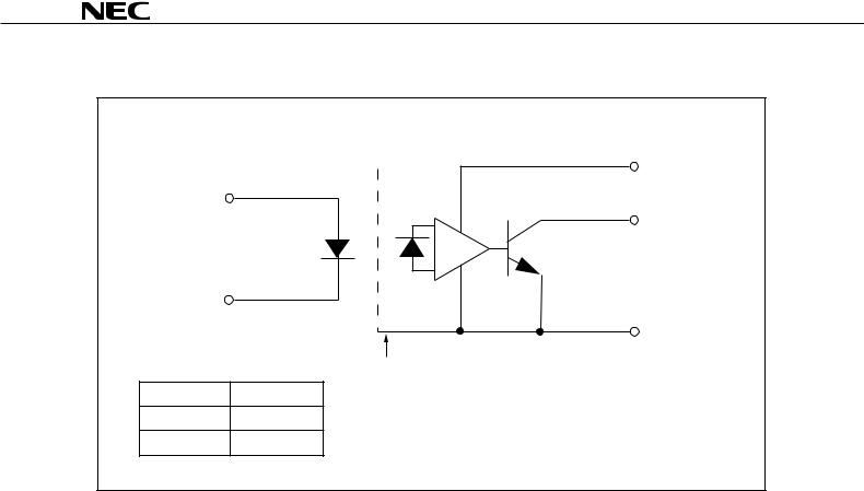
FUNCTIONAL DIAGRAM
|
8 |
|
2 |
|
6 |
|
3 |
|
5 |
|
Shield |
LED |
Output |
ON |
L |
OFF |
H |
Data Sheet P13981EJ2V0DS00 |
3 |

|
|
|
|
|
PS9613,PS9613L |
|
|
ORDERING INFORMATION |
|
|
|
|
|
|
|
|
|
|
|
|
|
Part Number |
Package |
Packing Style |
Safety Standards |
Application Part |
|
|
Approval |
Number*1 |
|
|||
|
|
|
|
|
|
|
|
PS9613 |
8-pin DIP |
Magazine case 50 pcs |
UL approved |
PS9613 |
|
|
|
|
|
|
|
|
|
PS9613L |
|
|
|
PS9613L |
|
|
|
|
|
|
|
|
|
PS9613L-E3 |
|
Embossed Tape 1 000 pcs/reel |
|
|
|
|
|
|
|
|
|
|
|
PS9613L-E4 |
|
|
|
|
|
|
|
|
|
|
|
|
|
PS9613-V |
|
Magazine case 50 pcs |
VDE0884 approved |
PS9613 |
|
|
|
|
|
|
|
|
|
PS9613L-V |
|
|
|
PS9613L |
|
|
|
|
|
|
|
|
|
PS9613L-V-E3 |
|
Embossed Tape 1 000 pcs/reel |
|
|
|
|
|
|
|
|
|
|
|
PS9613L-V-E4 |
|
|
|
|
|
|
|
|
|
|
|
|
*1 For the application of the Safety Standard, following part number should be used.
ABSOLUTE MAXIMUM RATINGS (TA = 25 °C, unless otherwise specified)
|
Parameter |
Symbol |
Ratings |
Unit |
|
|
|
|
|
Diode |
Forward Current |
IF |
25 |
mA |
|
|
|
|
|
|
Reverse Voltage |
VR |
3.0 |
V |
|
|
|
|
|
Detector |
Supply Voltage |
VCC |
−0.5 to +35 |
V |
|
|
|
|
|
|
Output Voltage |
VO |
−0.5 to +35 |
V |
|
|
|
|
|
|
Output Current |
IO |
15 |
mA |
|
|
|
|
|
|
Power Dissipation |
PC |
100 |
mW |
|
|
|
|
|
Isolation Voltage *1 |
BV |
5 000 |
Vr.m.s. |
|
|
|
|
|
|
Operating Ambient Temperature |
TA |
−40 to +100 |
°C |
|
|
|
|
|
|
Storage Temperature |
Tstg |
−55 to +125 |
°C |
|
|
|
|
|
|
*1 AC voltage for 1 minute at TA = 25 °C, RH = 60 % between input and output.
RECOMMENDED OPERATING CONDITIONS
Parameter |
Symbol |
MIN. |
TYP. |
MAX. |
Unit |
|
|
|
|
|
|
Forward Current |
IF |
10 |
|
20 |
mA |
|
|
|
|
|
|
Output Voltage |
VO |
0 |
|
30 |
V |
|
|
|
|
|
|
Supply Voltage |
VCC |
4.5 |
|
30 |
V |
|
|
|
|
|
|
LED Off Voltage |
VF |
0 |
|
0.8 |
V |
|
|
|
|
|
|
4 |
Data Sheet P13981EJ2V0DS00 |

PS9613,PS9613L
ELECTRICAL CHARACTERISTICS (TA = −40 to +100 °C, VCC = 15 V, unless otherwise specified)
|
Parameter |
Symbol |
Conditions |
MIN. |
TYP. *1 |
MAX. |
Unit |
|
|
|
|
|
|
|
|
Diode |
Forward Voltage |
VF |
IF = 10 mA |
1.3 |
1.65 |
2.1 |
V |
|
|
|
|
|
|
|
|
|
Reverse Current |
IR |
VR = 3 V |
|
|
200 |
μA |
|
|
|
|
|
|
|
|
|
Terminal Capacitance |
Ct |
V = 0 V, f = 1 MHz, TA = 25 °C |
|
30 |
|
pF |
|
|
|
|
|
|
|
|
Detector |
Low Level Output Voltage |
VOL |
IF = 10 mA, VCC = 5 V, IO = 2.4 mA |
|
0.13 |
0.6 |
V |
|
|
|
|
|
|
|
|
|
High Level Output Current |
IOH |
VCC = 30 V, VF = 0.8 V |
|
1.0 |
50 |
μA |
|
|
|
|
|
|
|
|
|
High Level Supply Current |
ICCH |
VCC = 30 V, VF = 0.8 V, VO = open |
|
0.6 |
1.3 |
mA |
|
|
|
|
|
|
|
|
|
Low Level Supply Current |
ICCL |
VCC = 30 V, IF = 10 mA, VO = open |
|
0.6 |
1.3 |
mA |
|
|
|
|
|
|
|
|
Coupled |
Threshold Input Current |
IFHL |
VO = 0.8 V, IO = 0.75 mA |
|
1.5 |
5.0 |
mA |
|
(H → L) |
|
|
|
|
|
|
|
|
|
|
|
|
|
|
|
Current Transfer Ratio (IC/IF) |
CTR |
IF = 10 mA, VO = 0.6 V |
44 |
110 |
|
% |
|
|
|
|
|
|
|
|
|
Isolation Resistance |
RI-O |
VI-O = 1 kVDC, RH = 40 to 60 %, |
1011 |
|
|
Ω |
|
|
|
TA = 25 °C |
|
|
|
|
|
|
|
|
|
|
|
|
|
Isolation Capacitance |
CI-O |
V = 0 V, f = 1 MHz, TA = 25 °C |
|
0.6 |
|
pF |
|
|
|
|
|
|
|
|
|
Propagation Delay Time |
tPHL |
IF = 10mA, RL = 20 kΩ, CL = 100 pF, |
|
250 |
500 |
ns |
|
(H → L) *2 |
|
VTHHL = 1.5 V, VTHLH = 2.0 V |
|
|
|
|
|
|
|
|
|
|
|
|
|
Propagation Delay Time |
tPLH |
|
|
520 |
750 |
|
|
(L → H) *2 |
|
|
|
|
|
|
|
|
|
|
|
|
|
|
|
Maximum Propagation |
tPLH−tPHL |
|
−200 |
270 |
650 |
|
|
Delays |
|
|
|
|
|
|
|
|
|
|
|
|
|
|
|
Pulse Width Distortion |
|tPHL−tPLH| |
|
|
270 |
650 |
|
|
(PWD) *2 |
|
|
|
|
|
|
|
|
|
|
|
|
|
|
|
Instantaneous Common |
CMH |
TA = 25 °C, IF = 0 mA, VO > 3.0 V, |
15 |
|
|
kV/μs |
|
Mode Rejection Voltage |
|
VCM = 1.5 kV, RL = 20 kΩ, |
|
|
|
|
|
(Output: High) *3 |
|
CL = 100 pF |
|
|
|
|
|
|
|
|
|
|
|
|
|
Instantaneous Common |
CML |
TA = 25 °C, IF = 10 mA, VO < 1.0 V, |
15 |
|
|
kV/μs |
|
Mode Rejection Voltage |
|
VCM = 1.5 kV, RL = 20 kΩ, |
|
|
|
|
|
(Output: Low) *3 |
|
CL = 100 pF |
|
|
|
|
|
|
|
|
|
|
|
|
Data Sheet P13981EJ2V0DS00 |
5 |
 Loading...