


DATA SHEET
PHOTOCOUPLER
PS9552,PS9552L1,PS9552L2,PS9552L3
2.5 A OUTPUT CURRENT, HIGH CMR IGBT GATE DRIVE PHOTOCOUPLER 8-PIN DIP PHOTOCOUPLER
−NEPOC Series−
DESCRIPTION
The PS9552, PS9552L1, PS9552L2 and PS9552L3 are optically coupled isolators containing a GaAlAs LED on the input side and a photo diode, a signal processing circuit and a power output transistor on the output side on one chip.
The PS9552 Series is designed specifically for high common mode transient immunity (CMR), high output current and high switching speed.
The PS9552 Series is suitable for driving IGBTs and MOS FETs.
The PS9552 Series is in a plastic DIP (Dual In-line Package).
The PS9552L1 is lead bending type for long creepage distance.
The PS9552L2 is lead bending type for long creepage distance (Gull-wing) for surface mount.
The PS9552L3 is lead bending type (Gull-wing) for surface mounting.
FEATURES
• Long creepage distance (8 mm MIN.: PS9552L1, PS9552L2) |
PIN CONNECTION |
• Large peak output current (2.5 A MAX., 2.0 A MIN.) |
|
|
(Top View) |
|
||
|
|
|
|
|
|
|
• High speed switching (tPLH, tPHL = 0.5 μs MAX.) |
8 |
7 |
6 |
5 |
1. NC |
|
• UVLO (Under Voltage Lock Out) protection with hysteresis |
|
|
|
|
2. |
Anode |
• High common mode transient immunity (CMH, CML = ±25 kV/μs MIN.) |
|
|
|
|
3. |
Cathode |
|
|
|
|
4. NC |
||
|
|
|
|
SHIELD |
||
• Ordering number of tape product: PS9552L2-E3: 1 000 pcs/reel |
|
|
|
6. |
VO |
|
|
|
|
|
5. |
VEE |
|
: PS9552L3-E3: 1 000 pcs/reel |
|
|
|
|
7. |
VO |
|
|
|
|
|
||
• Safety standards |
1 |
2 |
3 |
4 |
8. |
VCC |
• UL approved: No. E72422 |
|
|
|
|
|
|
• CSA approved: No. CA 101391 |
|
|
|
|
|
|
• BSI approved: No. 8937, 8938 |
|
|
|
|
|
|
• SEMKO approved: No. 615433 |
|
|
|
|
|
|
• NEMKO approved: No. P06207243 |
|
|
|
|
|
|
• DEMKO approved: No. 314091 |
|
|
|
|
|
|
• FIMKO approved: No. FI 22827 |
|
|
|
|
|
|
<R> |
• DIN EN60747-5-2 (VDE0884 Part2) approved: No. 40019182 (Option) |
APPLICATIONS
•IGBT, Power MOS FET Gate Driver
•Industrial inverter
•IH (Induction Heating)
The information in this document is subject to change without notice. Before using this document, please confirm that this is the latest version.
Not all products and/or types are available in every country. Please check with an NEC Electronics sales representative for availability and additional information.
Document No. PN10589EJ06V0DS (6th edition)
Date Published October 2008 NS |
|
2006, 2008 |
Printed in Japan |
The mark <R> shows major revised points. |
The revised points can be easily searched by copying an "<R>" in the PDF file and specifying it in the "Find what:" field.

PS9552,PS9552L1,PS9552L2,PS9552L3
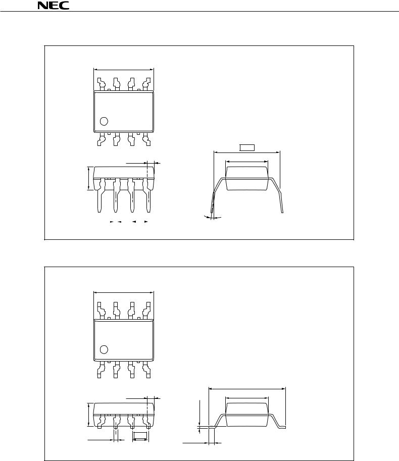
PACKAGE DIMENSIONS (UNIT: mm)
DIP Type
PS9552
9.25+0.5–0.25
8 |
5 |
1 |
4 |
7.62 |
|
1.01+0.4–0.2 |
6.5+0.5–0.1 |
3.5±0.2
0.5±0.15 |
2.54 |
0 to 15˚ |
|
||
|
|
Lead Bending Type (Gull-wing) For Surface Mount
PS9552L3
|
9.25+0.5–0.25 |
8 |
5 |
1 |
4 |
1.01+0–0..42
3.5±0.2
2.54 0.5±0.15 
0.635±0.15
0.74±0.25
9.65±0.4
6.5+0–0..51
2 |
Data Sheet PN10589EJ06V0DS |
PS9552,PS9552L1,PS9552L2,PS9552L3
Lead Bending Type For Long Creepage Distance
PS9552L1
9.25+0.5–0.25
8 |
5 |
1 |
4 |
10.16 |
|
1.01+0.4–0.2 |
6.5+0.5–0.1 |
3.5±0.2
|
|
|
|
|
|
|
|
|
|
|
0 to 15˚ |
|
|
|
|
|
|
|
|
|
|
|
|
0.5±0.15 |
|
|
|
|
|
|
|
2.54 |
|
|
|
|
|
|
|
|
|
|
|
||||
|
|
|
|
|
|
|
|
|
|
|
|
|
|
|
|
|
|
|
|
|
|
|
|
Lead Bending Type (Gull-wing) For Long Creepage Distance (Surface Mount)
PS9552L2
|
9.25+0.5–0.25 |
8 |
5 |
1 |
|
4 |
11.8±0.4 |
|
|
|
|
|
1.01+0–0..24 |
|
6.5+0–0..15 |
3.5±0.2 |
|
|
0.25±0.2 |
0.5±0.15 |
2.54 |
|
0.9±0.25 |
|
|
||
|
|
|
Data Sheet PN10589EJ06V0DS |
3 |
PS9552,PS9552L1,PS9552L2,PS9552L3
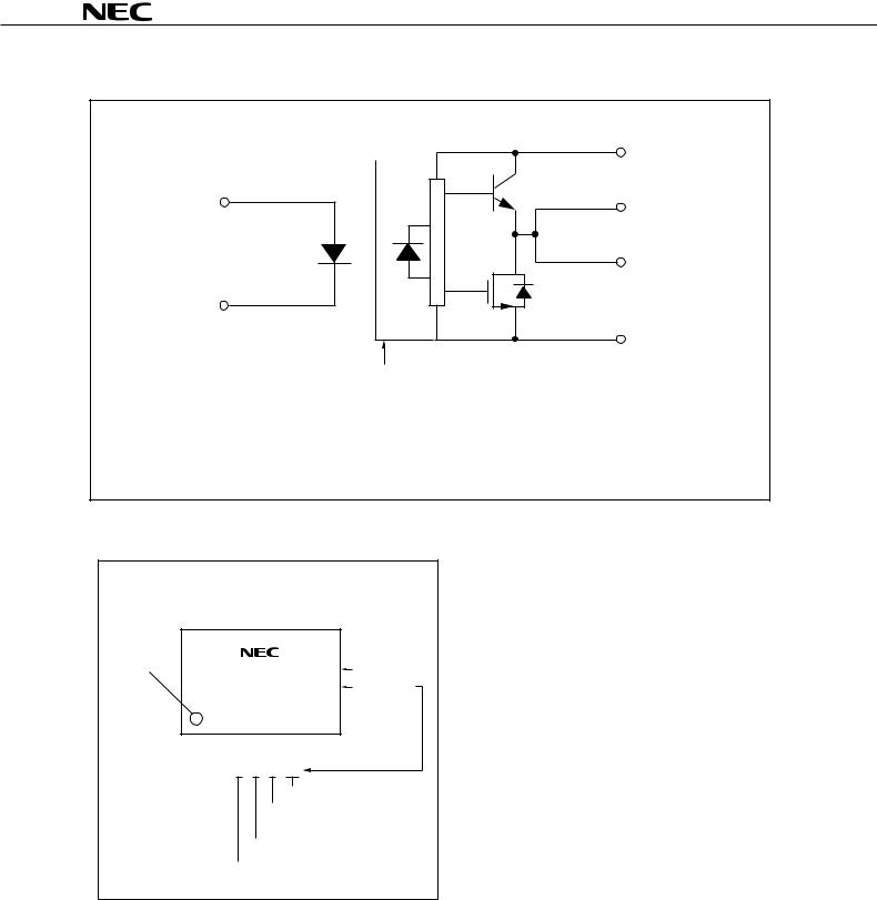
FUNCTIONAL DIAGRAM
|
|
8 |
|
(Tr. 1) |
|
2 |
|
7 |
|
|
|
|
(Tr. 2) |
6 |
|
|
3
5
|
|
|
SHIELD |
|
|
|
|
|
|
|
|
Input |
LED |
Tr. 1 |
|
Tr. 2 |
Output |
|
|
|
|
|
|
H |
ON |
ON |
|
OFF |
H |
|
|
|
|
|
|
L |
OFF |
OFF |
|
ON |
L |
|
|
|
|
|
|
MARKING EXAMPLE
No. 1 pin |
|
|
|
Mark |
9552 |
Type Number |
|
|
|||
|
NT831 |
Assembly Lot |
|
|
N T |
8 31 |
|
|
|
Week Assembled |
|
|
|
Year Assembled |
|
|
|
(Last 1 Digit) |
|
|
|
In-house Code |
|
|
Rank Code |
|
|
PHOTOCOUPLER CONSTRUCTION
|
Parameter |
PS9552, PS9552L3 |
PS9552L1, PS9552L2 |
|
|
|
|
|
Air Distance (MIN.) |
7 mm |
8 mm |
|
|
|
|
|
Outer Creepage Distance (MIN.) |
7 mm |
8 mm |
|
|
|
|
|
Isolation Distance (MIN.) |
0.4 mm |
0.4 mm |
4 |
|
|
|
|
Data Sheet PN10589EJ06V0DS |
||

PS9552,PS9552L1,PS9552L2,PS9552L3
ORDERING INFORMATION
Part Number |
Order Number |
Solder Plating |
Packing Style |
Safety Standard |
Application Part |
|
|
Specification |
|
Approval |
Number*1 |
|
|
|
|
|
|
PS9552 |
PS9552-AX |
Pb-Free |
Magazine case 50 pcs |
Standard products |
PS9552 |
|
|
|
|
|
|
PS9552L1 |
PS9552L1-AX |
(Ni/Pd/Au) |
|
(UL, CSA, BSI, |
PS9552L1 |
|
|
|
|
|
|
PS9552L2 |
PS9552L2-AX |
|
|
SEMKO, NEMKO, |
PS9552L2 |
|
|
|
|
|
|
PS9552L3 |
PS9552L3-AX |
|
|
DEMKO, FIMKO |
PS9552L3 |
|
|
|
|
|
|
PS9552L2-E3 |
PS9552L2-E3-AX |
|
Embossed Tape 1 000 pcs/reel |
approved) |
PS9552L2 |
|
|
|
|
|
|
PS9552L3-E3 |
PS9552L3-E3-AX |
|
|
|
PS9552L3 |
|
|
|
|
|
|
PS9552-V |
PS9552-V-AX |
|
Magazine case 50 pcs |
DIN EN60747-5-2 |
PS9552 |
|
|
|
|
|
|
PS9552L1-V |
PS9552L1-V-AX |
|
|
(VDE0884 Part2) |
PS9552L1 |
|
|
|
|
|
|
PS9552L2-V |
PS9552L2-V-AX |
|
|
Approved (Option) |
PS9552L2 |
|
|
|
|
|
|
PS9552L3-V |
PS9552L3-V-AX |
|
|
|
PS9552L3 |
|
|
|
|
|
|
PS9552L2-V-E3 |
PS9552L2-V-E3-AX |
|
Embossed Tape 1 000 pcs/reel |
|
PS9552L2 |
|
|
|
|
|
|
PS9552L3-V-E3 |
PS9552L3-V-E3-AX |
|
|
|
PS9552L3 |
|
|
|
|
|
|
*1 For the application of the Safety Standard, following part number should be used.
Data Sheet PN10589EJ06V0DS |
5 |

PS9552,PS9552L1,PS9552L2,PS9552L3
ABSOLUTE MAXIMUM RATINGS (TA = 25°C, unless otherwise specified)
|
Parameter |
Symbol |
Ratings |
Unit |
|
|
|
|
|
Diode |
Forward Current |
IF |
25 |
mA |
|
|
|
|
|
|
Peak Transient Forward |
IF (TRAN) |
1.0 |
A |
|
Current (Pulse Width < 1 μs) |
|
|
|
|
|
|
|
|
|
Reverse Voltage |
VR |
5 |
V |
|
|
|
|
|
Detector |
High Level Peak Output |
IOH (PEAK) |
2.5 |
A |
|
Current *1 |
|
|
|
|
|
|
|
|
|
Low Level Peak Output |
IOL (PEAK) |
2.5 |
A |
|
Current *1 |
|
|
|
|
|
|
|
|
|
Supply Voltage |
(VCC - VEE) |
0 to 35 |
V |
|
|
|
|
|
|
Output Voltage |
VO |
0 to VCC |
V |
|
|
|
|
|
|
Power Dissipation *2 |
PC |
250 |
mW |
|
|
|
|
|
Isolation Voltage *3 |
BV |
5 000 |
Vr.m.s. |
|
|
|
|
|
|
Total Power Dissipation *4 |
PT |
300 |
mW |
|
|
|
|
|
|
Operating Frequency *5 |
f |
50 |
kHz |
|
|
|
|
|
|
Operating Ambient Temperature |
TA |
−40 to +100 |
°C |
|
|
|
|
|
|
Storage Temperature |
Tstg |
−55 to +125 |
°C |
|
|
|
|
|
|
*1 Maximum pulse width = 10 μs, Maximum duty cycle = 0.2%
*2 Reduced to 4.8 mW/°C at TA = 70°C or more.
*3 AC voltage for 1 minute at TA = 25°C, RH = 60% between input and output. Pins 1-4 shorted together, 5-8 shorted together.
*4 Reduced to 5.4 mW/°C at TA = 70°C or more.
*5 IOH (PEAK) ≤ 2.0 A (≤ 0.3 μs), IOL (PEAK) ≤ 2.0 A (≤ 0.3 μs)
RECOMMENDED OPERATING CONDITIONS
Parameter |
Symbol |
MIN. |
TYP. |
MAX. |
Unit |
|
|
|
|
|
|
Supply Voltage |
(VCC - VEE) |
15 |
|
30 |
V |
|
|
|
|
|
|
Forward Current (ON) |
IF (ON) |
7 |
10 |
16 |
mA |
|
|
|
|
|
|
Forward Voltage (OFF) |
VF (OFF) |
−2 |
|
0.8 |
V |
|
|
|
|
|
|
Operating Ambient Temperature |
TA |
−40 |
|
100 |
°C |
|
|
|
|
|
|
6 |
Data Sheet PN10589EJ06V0DS |

PS9552,PS9552L1,PS9552L2,PS9552L3
ELECTRICAL CHARACTERISTICS (TA = −40 to +100°C, VCC = 15 to 30 V, IF (ON) = 7 to 16 mA, VF (OFF) = −2 to 0.8 V, VEE = GND, unless otherwise specified)
|
|
Parameter |
Symbol |
Conditions |
MIN. |
TYP.*1 |
MAX. |
Unit |
|
|
|
|
|
|
|
|
|
Diode |
Forward Voltage |
VF |
IF = 10 mA, TA = 25°C |
1.3 |
1.65 |
2.1 |
V |
|
|
|
|
|
|
|
|
|
|
|
|
Input Capacitance |
CIN |
f = 1 MHz, VF = 0 V, TA = 25°C |
|
60 |
|
pF |
|
|
|
|
|
|
|
|
|
Detector |
High Level Output Current |
IOH |
VO = (VCC − 4 V) *2 |
0.5 |
2.0 |
|
A |
|
|
|
|
|
|
|
|
|
|
|
|
|
|
VO = (VCC − 15 V) *3 |
2.0 |
|
|
|
|
|
|
|
|
|
|
|
|
|
|
Low Level Output Current |
IOL |
VO = (VEE + 2.5 V) *2 |
0.5 |
2.0 |
|
A |
|
|
|
|
|
|
|
|
|
|
|
|
|
VO = (VEE + 15 V) *3 |
2.0 |
|
|
|
|
|
|
|
|
|
|
|
|
|
|
High Level Output Voltage |
VOH |
IO = −100 mA *4 |
VCC − 3.5 |
VCC − 2.5 |
VCC − 1.5 |
V |
|
|
|
|
|
|
|
|
|
|
|
Low Level Output Voltage |
VOL |
IO = 100 mA |
|
0.1 |
0.5 |
V |
|
|
|
|
|
|
|
|
|
|
|
High Level Supply Current |
ICCH |
VO = open, IF = 7 to 16 mA |
|
2.0 |
5.0 |
mA |
|
|
|
|
|
|
|
|
|
|
|
Low Level Supply Current |
ICCL |
VO = open, VF = −2 to +0.8 V |
|
2.0 |
5.0 |
mA |
|
|
|
|
|
|
|
|
|
|
|
UVLO Threshold |
VUVLO+ |
VO > 5 V, IF = 10 mA |
11.0 |
12.3 |
13.5 |
V |
|
|
|
|
|
|
|
|
|
|
|
|
VUVLO− |
|
9.5 |
10.7 |
12.0 |
|
|
|
|
|
|
|
|
|
|
|
|
UVLO Hysteresis |
UVLOHYS |
VO > 5 V, IF = 10 mA |
|
1.6 |
|
V |
|
|
|
|
|
|
|
|
|
Coupled |
Threshold Input Current |
IFLH |
IO = 0 mA, VO > 5 V |
|
2.0 |
5.0 |
mA |
|
|
|
(L → H) |
|
|
|
|
|
|
|
|
|
|
|
|
|
|
|
|
|
Threshold Input Voltage |
VFHL |
IO = 0 mA, VO < 5 V |
0.8 |
|
|
V |
|
|
(H → L) |
|
|
|
|
|
|
|
|
|
|
|
|
|
|
|
*1 |
Typical values at TA = 25°C. |
|
|
|
|
|
|
|
*2 |
Maximum pulse width = 50 μs, Maximum duty cycle = 0.5%. |
|
|
|
|
|||
*3 |
Maximum pulse width = 10 μs, Maximum duty cycle = 0.2% |
|
|
|
|
|||
*4 VOH is measured with the DC load current in this testing (Maximum pulse width = 2 ms, Maximum duty cycle =
20%).
Data Sheet PN10589EJ06V0DS |
7 |
 Loading...