


DATA SHEET
PHOTOCOUPLER
PS8701
HIGH NOISE REDUCTION HIGH-SPEED ANALOG OUTPUT TYPE
5-PIN SOP PHOTOCOUPLER
DESCRIPTION
The PS8701 is an optically coupled isolator containing a GaAlAs LED on the light emitting diode (input side) and a PIN photodiode and a high-speed amplifier transistor on the output side on one chip.
This is a plastic SOP (Small Out-line Package) type for high density applications.
FEATURES
•High common mode transient immunity (CMH, CML = ±10 kV/μs MIN.)
•High supply voltage (VCC = 35 V)
•High isolation voltage (BV = 2 500 Vr.m.s.)
•High-speed response (tPHL = 0.8 μs MAX., tPLH = 1.2 μs MAX.)
•Taping product number (PS8701-E3, E4, F3, F4)
APPLICATIONS
•Computer and peripheral manufactures
•General purpose inverter
•Substitutions for relays and pulse transformers
•Power supply
PACKAGE DIMENSIONS in millimeters
4.5 MAX.
TOP VIEW
5 4 3
1. Anode
2. Cathode
3. GND
4. VO
5. VCC
1 2
7.0±0.3
MAX. |
2.0 |
2.3 |
|
|
0.1±0.1 |
|
|
4.4 |
1.3 |
|
|
+0.10 –0.05 |
|
|
|
0.15 |
|
1.27 |
1.2 MAX. |
0.5±0.3 |
|
0.4–0+0..0510 |
0.25 M |
The information in this document is subject to change without notice.
Document No. P12846EJ1V0DS00 (1st edition)
Date Published August 1997 NS |
© |
1997 |
Printed in Japan |

PS8701
ABSOLUTE MAXIMUM RATINGS (TA = 25 °C, unless otherwise specified)
|
Parameter |
Symbol |
Ratings |
Unit |
|
|
|
|
|
Diode |
Forward Current |
IF |
25 |
mA |
|
|
|
|
|
|
Reverse Voltage |
VR |
3.0 |
V |
|
|
|
|
|
|
Power Dissipation |
PD |
45 |
mW |
|
|
|
|
|
Detector |
Supply Voltage |
VCC |
35 |
V |
|
|
|
|
|
|
Output Voltage |
VO |
35 |
V |
|
|
|
|
|
|
Output Current |
IO |
8.0 |
mA |
|
|
|
|
|
|
Power Dissipation |
PC |
100 |
mW |
|
|
|
|
|
Isolation Voltage*1 |
BV |
2 500 |
Vr.m.s. |
|
|
|
|
|
|
Operating Ambient Temperature |
TA |
–55 to +100 |
°C |
|
|
|
|
|
|
Storage Temperature |
Tstg |
–55 to +125 |
°C |
|
|
|
|
|
|
*1 AC voltage for 1 minute at TA = 25 °C, RH = 60 % between input and output
ELECTRICAL CHARACTERISTICS (TA = 25 °C)
|
Parameter |
Symbol |
Conditions |
MIN. |
TYP. |
MAX. |
Unit |
|
|
|
|
|
|
|
|
Diode |
Forward Voltage |
VF |
IF = 16 mA |
|
1.7 |
2.2 |
V |
|
|
|
|
|
|
|
|
|
Reverse Current |
IR |
VR = 3 V |
|
|
10 |
μA |
|
|
|
|
|
|
|
|
|
Forward Voltage |
VF/ T |
IF = 16 mA |
|
−1.6 |
|
mV/°C |
|
Temperature Coefficient |
|
|
|
|
|
|
|
|
|
|
|
|
|
|
|
Terminal Capacitance |
Ct |
V = 0 V, f = 1 MHz |
|
60 |
|
pF |
|
|
|
|
|
|
|
|
Detector |
High Level Output Current |
IOH (1) |
IF = 0 mA, VCC = VO = 5.5 V |
|
3 |
500 |
nA |
|
|
|
|
|
|
|
|
|
High Level Output Current |
IOH (2) |
IF = 0 mA, VCC = VO = 30 V |
|
|
100 |
μA |
|
|
|
|
|
|
|
|
|
Low Level Output Voltage |
VOL |
IF = 16 mA, VCC = 4.5 V, IO = 1.2 mA |
|
0.1 |
0.4 |
V |
|
|
|
|
|
|
|
|
|
Low Level Supply Current |
ICCL |
IF = 16 mA, VO = open, VCC = 30 V |
|
50 |
|
μA |
|
|
|
|
|
|
|
|
|
High Level Supply Current |
ICCH |
IF = 0 mA, VO = open, VCC = 30 V |
|
0.01 |
2 |
|
|
|
|
|
|
|
|
|
Coupled |
Current Transfer Ratio |
CTR |
IF = 16 mA, VCC = 4.5 V, VO = 0.4 V |
15 |
20 |
35 |
% |
|
|
|
|
|
|
|
|
|
Isolation Resistance |
RI-O |
VI-O = 1 kVDC, RH = 40 to 60 % |
1011 |
|
|
Ω |
|
|
|
|
|
|
|
|
|
Isolation Capacitance |
CI-O |
V = 0 V, f = 1 MHz |
|
0.4 |
|
pF |
|
|
|
|
|
|
|
|
|
Propagation Delay Time |
tPHL |
IF = 16 mA, VCC = 5 V, RL = 2.2 kΩ, |
|
0.5 |
0.8 |
μs |
|
(H → L)*1 |
|
CL = 15 pF |
|
|
|
|
|
|
|
|
|
|
|
|
|
Propagation Delay Time |
tPLH |
|
|
0.6 |
1.2 |
|
|
(L → H)*1 |
|
|
|
|
|
|
|
|
|
|
|
|
|
|
|
Common Mode |
CMH |
IF = 0 mA, VCC = 5 V, RL = 4.1 kΩ, |
10 |
|
|
kV/μs |
|
Transient Immunity at |
|
VCM = 1.5 kV |
|
|
|
|
|
High Level Output*2 |
|
|
|
|
|
|
|
|
|
|
|
|
|
|
|
Common Mode |
CML |
IF = 16 mA, VCC = 5 V, RL = 4.1 kΩ, |
−10 |
|
|
|
|
Transient Immunity at |
|
VCM = 1.5 kV |
|
|
|
|
|
Low Level Output*2 |
|
|
|
|
|
|
|
|
|
|
|
|
|
|
2
PS8701
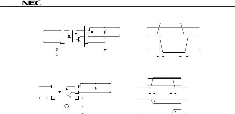
*1 |
Test circuit for propagation delay time |
|
|
||
|
|
|
|
|
Input |
|
Pulse input |
|
|
VCC = 5 V |
50 % |
(Pulse width = 100 μs, |
|
0.1 μF |
RL = 2.2 kΩ |
|
|
|
|
VO (Monitor) |
|
||
Duty cycle = 1/10) |
|
|
5 V |
||
|
|
CL = 15 pF |
|||
|
|
|
|
|
|
|
Input |
|
|
|
Output |
|
|
|
|
|
|
|
(Monitor) |
47 |
Ω |
|
1.5 V |
|
|
|
VOL |
||
|
|
|
|
|
|
|
|
|
|
|
|
|
|
|
|
|
|
|
|
|
|
|
|
|
|
|
|
|
|
|
tPHL |
|
|
|
|
|
|
|
|
|
tPLH |
|
|
|
|
|
||||||
|
|
|
|
|
|
|
|
|
|
|
|
|
|
|
|
|
|
|
|
|
||||||||||||||||||||||||||
CL is approximately 15 pF which includes probe and stray wiring capacitance |
|
|
|
|
|
|
|
|
|
|
|
|
|
|
|
|
|
|||||||||||||||||||||||||||||
*2 Test circuit for common mode transient immunity |
|
|
|
|
|
|
|
|
|
|
|
|
|
|
|
|
|
|
|
|
|
|
1.5 kV |
|||||||||||||||||||||||
|
|
|
|
|
|
|
|
|
|
|
|
|
|
|
|
|
|
|
|
|
VCM 90 % |
|
|
|
|
|
|
|
|
|
|
|
|
|
|
|
|
|
||||||||
|
|
|
|
|
|
|
|
|
|
|
|
|
|
|
|
|
|
|
|
VCC = 5 V |
|
|
|
|
|
|
|
|
|
|
|
|
|
|
|
|
|
|
|
|
|
|||||
|
|
|
|
|
|
|
|
|
|
|
|
|
|
|
|
|
|
|
|
|
|
|
|
|
|
|
|
|
|
|
|
|
|
|
|
|
|
|||||||||
IF |
|
|
|
|
|
|
|
|
|
|
|
|
|
|
|
|
0.1 μF |
10 % |
|
|
|
|
|
|
|
|
|
|
|
|
|
|
|
|
|
|
|
|
|
|
0 V |
|||||
|
|
|
|
|
|
|
|
|
|
|
|
|
|
|
|
|
|
|
|
|
|
|
|
|
|
|
|
|
|
|
|
|
|
|
|
|
|
|||||||||
|
|
|
|
|
|
|
|
|
|
|
|
|
|
|
|
|
|
|
RL = 4.1 kΩ |
|
tr |
|
|
|
|
|
|
|
|
|
|
|
|
tf |
|
|
|
|
|
|
|
|
|
|||
|
|
|
|
|
|
|
|
|
|
|
|
|
|
|
|
|
|
|
|
|
|
|
|
|
|
|
|
|
|
|
|
|
|
|
|
|
|
|
||||||||
|
|
|
|
|
|
|
|
|
|
|
|
|
|
|
|
|
|
|
|
VO (Monitor) |
|
|
|
|
|
|
|
|
|
|
|
|
|
|
|
|
||||||||||
|
|
|
|
|
|
|
|
|
|
|
|
|
|
|
|
|
|
|
|
|
VO |
|
|
|
|
|
|
|
|
|
|
|
|
|
|
|
|
|
|
|
|
|
5 V |
|||
|
|
|
|
|
|
|
|
|
|
|
|
|
|
|
|
|
|
|
|
|
|
|
|
|
|
|
|
|
|
|
|
|
|
|
|
|||||||||||
|
|
|
|
|
|
|
|
|
|
|
|
|
|
|
|
|
|
|
|
|
(IF = 0 mA) |
|
|
|
|
|
|
|
|
|
|
|
|
|
|
|
|
|
|
|
2 V |
|||||
|
|
|
|
|
|
|
|
|
|
|
|
|
|
|
|
|
|
|
|
|
|
|
|
|
|
|
|
|
|
|
|
|
|
|||||||||||||
|
|
|
|
|
|
VCM |
|
|
|
VO |
|
|
|
|
|
|
|
|
|
|
|
|
|
|
|
|
|
|
|
0.8 V |
||||||||||||||||
|
|
|
|
|
|
|
|
|
|
|
|
|
|
|
|
|
|
|
|
|
|
|
|
|
|
|
|
|
|
VOL |
||||||||||||||||
|
|
|
|
|
|
|
|
|
|
|
|
|
|
|
|
|
|
|
|
|
|
|
|
|
|
|
|
|
|
|
|
|
|
|
|
|
|
|
|
|
|
|||||
|
|
|
|
|
|
|
|
|
|
|
|
|
|
|
|
|
|
|
|
|
|
|
|
|
|
|
|
|
|
|
|
|
|
|
|
|||||||||||
|
|
|
|
|
|
|
|
|
|
|
|
|
|
|
|
|
|
|
|
|
(IF = 16 mA) |
|
|
|
|
|
|
|
|
|
|
|
|
|
|
|
|
|
|
|
|
|
|
|
||
|
|
|
|
|
|
|
|
|
|
|
|
|
|
|
|
|
|
|
|
|
|
|
|
|
|
|
|
|
|
|
|
|
|
|
|
|
|
|
|
|||||||
USAGE CAUTIONS
1.This product is weak for static electricity by designed with high-speed integrated circuit so protect against static electricity when handling.
2.By-pase capacitor of more than 0.1 μF is used between VCC and GND near device.
3
 Loading...