


DATA SHEET
PHOTOCOUPLER
PS8502,PS8502L1,PS8502L2,PS8502L3
HIGH SPEED ANALOG OUTPUT TYPE
8 mm CREEPAGE 8-PIN PHOTOCOUPLER −NEPOC Series−
DESCRIPTION
The PS8502, PS8502L1, PS8502L2 and PS8502L3 are 8-pin high speed photocouplers containing a GaAIAs LED on input side and a PN photodiode and a high speed amplifier transistor on output side on one chip. The PS8502 is in a plastic DIP (Dual In-line Package) with 8 mm creepage distance product.
The PS8502L1 is lead bending type for long creepage distance.
The PS8502L2 is lead bending type for long creepage distance (Gull-wing) for surface mount.
The PS8502L3 is lead bending type (Gull-wing) for surface mounting.
FEATURES
•Long creepage distance (8 mm MIN.: PS8502L1, PS8502L2)
•High common mode transient immunity (CMH, CML = ±15 kV/μs MIN.)
•High supply voltage (VCC = 35 V MAX.)
•High speed response (tPHL, tPLH = 0.8 μs MAX.)
•High isolation voltage (BV = 5 000 Vr.m.s.)
•TTL, CMOS compatible with a resistor
•Ordering number of tape product: PS8502L2-E3: 1 000 pcs/reel
:PS8502L3-E3: 1 000 pcs/reel
|
PIN CONNECTION |
|||||
|
|
(Top |
|
View) |
|
|
8 |
7 |
6 |
5 |
|
1. NC |
|
|
2. |
Anode |
||||
|
|
|
|
|
||
|
|
|
|
SHIELD |
3. |
Cathode |
|
|
|
|
4. NC |
||
|
|
|
|
|
||
|
|
|
|
|
5. |
Emitter |
|
|
|
|
|
6. |
VO |
1 |
2 |
3 |
4 |
|
7. NC |
|
|
8. |
VCC |
||||
|
|
|
|
|
||
•Pb-Free product
•Safety standards
•UL approved: File No. E72422
•CSA approved: No. CA 101391
•BSI approved: No. 8937, 8938
•SEMKO approved: No. 615433
•NEMKO approved: No. P06207243
•DEMKO approved: No. 314091
•FIMKO approved: No. FI 22827
•DIN EN60747-5-2 (VDE0884 Part2) approved (Option)
APPLICATIONS
•Interface for measurement or control equipment
•Substitutions for relays and pulse transformers
•Modem, communications device
•General purpose inverter
The information in this document is subject to change without notice. Before using this document, please confirm that this is the latest version.
Not all products and/or types are available in every country. Please check with an NEC Electronics sales representative for availability and additional information.
Document No. PN10657EJ03V0DS (3rd edition)
Date Published August 2008 NS |
|
2007, 2008 |
Printed in Japan |
The mark <R> shows major revised points. |
The revised points can be easily searched by copying an "<R>" in the PDF file and specifying it in the "Find what:" field.

PS8502,PS8502L1,PS8502L2,PS8502L3
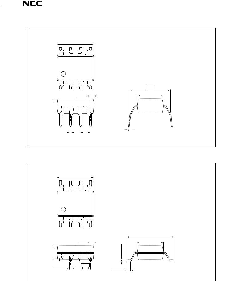
PACKAGE DIMENSIONS (UNIT: mm)
DIP Type
PS8502
9.25+0.5–0.25
1.01+0–0..42
7.62
6.5+0–0..51
3.5±0.2
0.5±0.15 |
2.54 |
0 to 15˚ |
|
||
|
|
Lead Bending Type (Gull-wing) For Surface Mount
PS8502L3
9.25+0.5–0.25
|
|
1.01+0–0..24 |
3.5±0.2 |
|
0.635±0.15 |
|
0.5±0.15 |
2.54 |
|
0.74±0.25 |
|
|
|
9.65±0.4
6.5+0–0..51
2 |
Data Sheet PN10657EJ03V0DS |
PS8502,PS8502L1,PS8502L2,PS8502L3
Lead Bending Type For Long Creepage Distance
PS8502L1
9.25+0.5–0.25
|
10.16 |
1.01+0–0..24 |
6.5+0–0..15 |
3.5±0.2
|
|
|
|
|
|
|
|
|
|
|
0 to 15˚ |
|
|
|
|
|
|
|
|
|
|
|
|
0.5±0.15 |
|
|
|
|
|
|
|
2.54 |
|
|
|
|
|
|
|
|
|
|
|
||||
|
|
|
|
|
|
|
|
|
|
|
|
|
|
|
|
|
|
|
|
|
|
|
|
Lead Bending Type For Long Creepage Distance (Gull-wing) For Surface Mount
PS8502L2
9.25+0.5–0.25
|
|
11.8±0.4 |
|
1.01+0–0..24 |
6.5+0–0..15 |
3.5±0.2 |
|
0.25±0.2 |
0.5±0.15 |
2.54 |
0.9±0.25 |
|
||
|
|
Data Sheet PN10657EJ03V0DS |
3 |
PS8502,PS8502L1,PS8502L2,PS8502L3
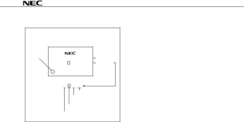
<R> MARKING EXAMPLE
No. 1 pin |
|
|
Mark |
8502 |
Type Number |
|
||
N 831 |
Assembly Lot |
|
N |
8 31 |
|
|
Week Assembled |
|
|
Year Assembled |
|
|
(Last 1 Digit) |
|
|
In-house Code |
|
|
(L or T) |
|
Rank Code |
|
|
PHOTOCOUPLER CONSTRUCTION
Parameter |
PS8502, PS8502L3 |
PS8502L1, PS8502L2 |
|
|
|
Air Distance (MIN.) |
7 mm |
8 mm |
|
|
|
Outer Creepage Distance (MIN.) |
7 mm |
8 mm |
|
|
|
Isolation Distance (MIN.) |
0.4 mm |
0.4 mm |
|
|
|
4 |
Data Sheet PN10657EJ03V0DS |

PS8502,PS8502L1,PS8502L2,PS8502L3
ORDERING INFORMATION
Part Number |
Order Number |
Solder Plating |
Packing Style |
Safety Standard |
Application Part |
|
|
Specification |
|
Approval |
Number*1 |
|
|
|
|
|
|
PS8502 |
PS8502-AX |
Pb-Free |
Magazine case 50 pcs |
Standard products |
PS8502 |
|
|
|
|
|
|
PS8502L1 |
PS8502L1-AX |
(Ni/Pd/Au) |
|
(UL, CSA, BSI, |
PS8502L1 |
|
|
|
|
|
|
PS8502L2 |
PS8502L2-AX |
|
|
SEMKO, NEMKO, |
PS8502L2 |
|
|
|
|
|
|
PS8502L3 |
PS8502L3-AX |
|
|
DEMKO, FIMKO |
PS8502L3 |
|
|
|
|
|
|
PS8502L2-E3 |
PS8502L2-E3-AX |
|
Embossed Tape 1 000 pcs/reel |
approved) |
PS8502L2 |
|
|
|
|
|
|
PS8502L3-E3 |
PS8502L3-E3-AX |
|
|
|
PS8502L3 |
|
|
|
|
|
|
PS8502-V |
PS8502-V-AX |
|
Magazine case 50 pcs |
DIN EN60747-5-2 |
PS8502 |
|
|
|
|
|
|
PS8502L1-V |
PS8502L1-V-AX |
|
|
(VDE0884 Part2) |
PS8502L1 |
|
|
|
|
|
|
PS8502L2-V |
PS8502L2-V-AX |
|
|
Approved (Option) |
PS8502L2 |
|
|
|
|
|
|
PS8502L3-V |
PS8502L3-V-AX |
|
|
|
PS8502L3 |
|
|
|
|
|
|
PS8502L2-V-E3 |
PS8502L2-V-E3-AX |
|
Embossed Tape 1 000 pcs/reel |
|
PS8502L2 |
|
|
|
|
|
|
PS8502L3-V-E3 |
PS8502L3-V-E3-AX |
|
|
|
PS8502L3 |
|
|
|
|
|
|
*1 For the application of the Safety Standard, following part number should be used.
ABSOLUTE MAXIMUM RATINGS (TA = 25°C, unless otherwise specified)
|
Parameter |
Symbol |
Ratings |
Unit |
|
|
|
|
|
Diode |
Forward Current *1 |
IF |
25 |
mA |
|
|
|
|
|
|
Reverse Voltage |
VR |
5 |
V |
|
|
|
|
|
Detector |
Supply Voltage |
VCC |
35 |
V |
|
|
|
|
|
|
Output Voltage |
VO |
35 |
V |
|
|
|
|
|
|
Output Current |
IO |
8 |
mA |
|
|
|
|
|
|
Power Dissipation *2 |
PC |
100 |
mW |
|
|
|
|
|
Isolation Voltage *3 |
BV |
5 000 |
Vr.m.s. |
|
|
|
|
|
|
Operating Ambient Temperature |
TA |
−55 to +100 |
°C |
|
|
|
|
|
|
Storage Temperature |
Tstg |
−55 to +125 |
°C |
|
|
|
|
|
|
*1 Reduced to 0.33 mA/°C at TA = 70°C or more.
*2 Reduced to 2.0 mW/°C at TA = 75°C or more.
*3 AC voltage for 1 minute at TA = 25°C, RH = 60% between input and output. Pins 1-4 shorted together, 5-8 shorted together.
Data Sheet PN10657EJ03V0DS |
5 |

PS8502,PS8502L1,PS8502L2,PS8502L3
ELECTRICAL CHARACTERISTICS (TA = 25°C)
|
Parameter |
Symbol |
Conditions |
MIN. |
TYP.*1 |
MAX. |
Unit |
|
|
|
|
|
|
|
|
Diode |
Forward Voltage |
VF |
IF = 16 mA |
|
1.7 |
2.2 |
V |
|
|
|
|
|
|
|
|
|
Reverse Current |
IR |
VR = 3 V |
|
|
10 |
μA |
|
|
|
|
|
|
|
|
|
Forward Voltage |
VF/ TA |
IF = 16 mA |
|
−2.1 |
|
mV/°C |
|
Temperature Coefficent |
|
|
|
|
|
|
|
|
|
|
|
|
|
|
|
Terminal Capacitance |
Ct |
V = 0 V, f = 1 MHz |
|
60 |
|
pF |
|
|
|
|
|
|
|
|
Detector |
High Level Output Current |
IOH (1) |
IF = 0 mA, VCC = VO = 5.5 V |
|
3 |
500 |
nA |
|
|
|
|
|
|
|
|
|
High Level Output Current |
IOH (2) |
IF = 0 mA, VCC = VO = 35 V |
|
|
100 |
μA |
|
|
|
|
|
|
|
|
|
Low Level Output Voltage |
VOL |
IF = 16 mA, VCC = 4.5 V, IO = 2.4 mA |
|
0.15 |
0.4 |
V |
|
|
|
|
|
|
|
|
|
Low Level Supply Current |
ICCL |
IF = 16 mA, VO = Open, VCC = 35 V |
|
150 |
|
μA |
|
|
|
|
|
|
|
|
|
High Level Supply Current |
ICCH |
IF = 0 mA, VO = Open, VCC = 35 V |
|
0.01 |
1 |
μA |
|
|
|
|
|
|
|
|
Coupled |
Current Transfer Ratio |
CTR |
IF = 16 mA, VCC = 4.5 V, VO = 0.4 V |
15 |
|
|
% |
|
|
|
|
|
|
|
|
|
Isolation Resistance |
RI-O |
VI-O = 1 kVDC |
1011 |
|
|
Ω |
|
|
|
|
|
|
|
|
|
Isolation Capacitance |
CI-O |
V = 0 V, f = 1 MHz |
|
0.7 |
|
pF |
|
|
|
|
|
|
|
|
|
Propagation Delay Time |
tPHL |
IF = 16 mA, VCC = 5 V, RL = 1.9 kΩ |
|
0.22 |
0.8 |
μs |
|
(H → L)*2 |
|
|
|
|
|
|
|
|
|
|
|
|
|
|
|
Propagation Delay Time |
tPLH |
IF = 16 mA, VCC = 5 V, RL = 1.9 kΩ |
|
0.35 |
0.8 |
μs |
|
(L → H)*2 |
|
|
|
|
|
|
|
|
|
|
|
|
|
|
|
Common Mode |
CMH |
IF = 0 mA, VCC = 5 V, VCM = 1.5 kV, |
15 |
|
|
kV/μs |
|
Transient Immunity at High |
|
RL = 4.1 kΩ |
|
|
|
|
|
Level Output*3 |
|
|
|
|
|
|
|
|
|
|
|
|
|
|
|
Common Mode |
CML |
IF = 16 mA, VCC = 5 V, VCM = 1.5 kV, |
−15 |
|
|
kV/μs |
|
Transient Immunity at Low |
|
RL = 4.1 kΩ |
|
|
|
|
|
Level Output*3 |
|
|
|
|
|
|
|
|
|
|
|
|
|
|
6 |
Data Sheet PN10657EJ03V0DS |
 Loading...