


COP413C
查询COP313C供应商
COP413C/COP413CH/COP313C/COP313CH
Single-Chip CMOS Microcontrollers
COP413C/COP413CH/COP313C/COP313CH Single-Chip CMOS Microcontrollers
November 1990
General Description
The COP413C, COP413CH, COP313C, and COP313CH fully static, single-chip CMOS microcontrollers are members of
the COPS
TM
family, fabricated using double-poly, silicongate CMOS technology. These controller-oriented processors are complete microcomputers containing all system
timing, internal logic, ROM, RAM, and I/O necessary to implement dedicated control functions in a variety of applications. Features include single supply operation, with an instruction set, internal architecture, and I/O scheme designed to facilitate keyboard input, display output, and BCD
data manipulation. The COP413CH is identical to the
COP413C except for operating voltage and frequency. They
are an appropriate choice for use in numerous human interface control environments. Standard test procedures and
reliable high-density fabrication techniques provide a customized controller-oriented processor at a low end-product
cost.
The COP313C/COP313CH is the extended temperature
range version of the COP413C/COP413CH.
For emulation use the ROMless COP404C.
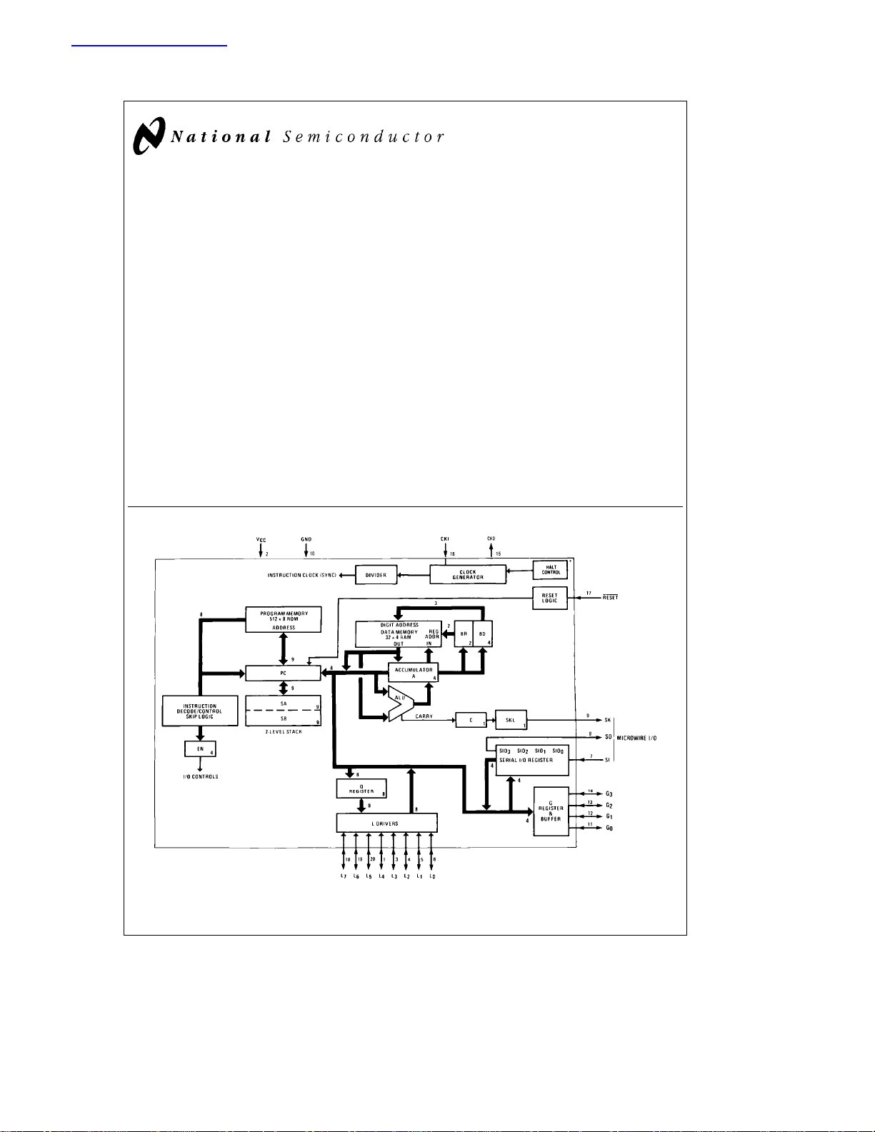
Block Diagram
Features
Y
Lowest power dissipation (40 mW typical)
Y
Low cost
Y
Power-saving HALT Mode
Y
Powerful instruction set
Y
512 x 8 ROM, 32x4RAM
Y
15 I/O lines
Y
Two-level subroutine stack
Y
DC to 4 ms instruction time
Y
Single supply operation (3V to 5.5V)
Y
General purpose and TRI-STATEÉoutputs
Y
Internal binary counter register with MICROWIRE
compatible serial I/O
Y
Software/hardware compatible with other members of
the COP400 family
Y
Extended temperature (b40§Ctoa85§C) devices
available
TM
TL/DD/8537– 1
FIGURE 1. COP413C/413CH
TRI-STATEÉis a registered trademark of National Semiconductor Corp.
TM
COPS
, MICROWIRETMand STARPLEXTMare trademarks of National Semiconductor Corp.
C
1995 National Semiconductor Corporation RRD-B30M105/Printed in U. S. A.
TL/DD/8537
COP413C/COP413CH
Absolute Maximum Ratings
If Military/Aerospace specified devices are required,
please contact the National Semiconductor Sales
Office/Distributors for availability and specifications.
Supply Voltage 6V
Voltage at Any Pin
b
0.3V to V
CC
a
0.3V
Total Allowable Source Current 25 mA
Total Allowable Sink Current 25 mA
DC Electrical Characteristics 0
CsT
§
A
Parameter Conditions
Operating Voltage 3.0 5.5 4.5 5.5 V
Power Supply Ripple (Notes 4, 5) 0.1 V
Supply Current (Note 1) V
HALT Mode Current (Note 2) V
e
CC
e
V
CC
(tcis inst. cycle)
e
CC
e
V
CC
5.0V, t
3.0V, t
5.0V, F
3.0V, F
e
Min 500 2000 mA
c
e
Min 300 mA
c
e
0 kHz 30 30 mA
I
e
0 kHz 10 mA
I
Input Voltage Levels
RESET
, CKI
Logic High 0.9 V
Logic Low 0.1 V
All Other Inputs
Logic High 0.7 V
Logic Low 0.2 V
RESET, SI Input Leakage
Input Capacitance (Notes 5, 6) 7 7 pF
Output Voltage Levels
(SO, SK, L Port)
Logic High I
Logic Low I
eb
10 mAV
OH
e
10 mA 0.2 0.2 V
OL
Output Current Levels
Sink (Note 3) V
Source (SO, SK, L Port) V
Source (G Port) V
CC
CC
CC
e
e
e
Min, V
Min, V
Min, V
OUT
OUT
OUT
e
e
e
Allowable Sink/Source
Current Per Pin (Note 3) 5 5 mA
TRI-STATE Leakage
Current
Operating Temperature Range 0
Storage Temperature Range
Note:
Absolute maximum ratings indicate limits beyond
which damage to the device may occur. DC and AC electrical specifications are not ensured when operating the device at absolute maximum ratings.
s
a
70§C unless otherwise specified
COP413C COP413CH
Min Max Min Max
CC
0.9 V
CC
CC
1
2
CC
0.7 V
CC
b
1
b
0.2 V
CC
b
0.5 mA
b
30
b
2
V
0V
0V
CC
CC
CC
b
1
b
0.2 V
CC
a
0.2 1.2 mA
b
0.1
b
8
b
2
b
150
a
Ctoa70§C
§
b
65§Ctoa150§C
0.1 V
CC
0.1 V
CC
0.2 V
CC
a
1 mA
b
330 mA
a
2 mA
Units
V
V
V
V
V
2
COP413C/COP413CH
AC Electrical Characteristics
Parameter Conditions
0§CsT
s
70§C unless otherwise specified
A
COP413C COP413CH
Min Max Min Max
Units
Instruction Cycle Time 16 DC 4 DC ms
Operating CKI Frequency
Instruction Cycle Time Re30kg5%, V
RC Oscillator
d
4C
Instruction Cycle Time Re56kg5%, V
RC Oscillatord4 (Note 6) Ce100 pFg5%
d
8 Mode DC 500 DC 2000 kHz
e
5V 8 16 ms
e
82 pFg5%
CC
e
5V 16 32 16 32 ms
CC
Duty Cycle (Note 5) FieMax freq ext clk 40 60 40 60 %
Rise Time (Note 5) FieMax freq ext clk 60 60 ns
Fall Time (Note 5) FieMax freq ext clk 40 40 ns
Inputs (See
t
SETUP
Figure 3
)
G Inputs tc/4a2.8 tc/4a0.7 ms
SI Input 1.2 0.3 ms
L Inputs 6.8 1.7 ms
t
HOLD
Output Propagation V
Delay R
t
PD1,tPD0
Note 1: Supply current is measured after running for 2000 cycle times with a square-wave clock on CKI, CKO open, and all other pins pulled to VCCwith 5k
resistors.
Note 2: The Halt mode will stop CKI from oscillating.
Note 3: SO output sink current must be limited to keep V
Note 4: Voltage change must be less than 0.5V ina1msperiod.
Note 5: This parameter is only sampled and not 100% tested.
Note 6: Variation due to the device included.
OUT
L
e
e
5k
e
1.5, C
100 pF
L
less tha 0.2 VCCwhen part is running in order to prevent entering test mode.
OL
1.0 0.25 ms
4.0 1.0 ms
3
COP313C/COP313CH
Absolute Maximum Ratings
If Military/Aerospace specified devices are required,
please contact the National Semiconductor Sales
Office/Distributors for availability and specifications.
Supply Voltage 6V
Voltage at Any Pin
Total Allowable Source Current 25 mA
b
0.3V to V
CC
a
0.3V
Total Allowable Sink Current 25 mA
Operating Temperature Range
Storage Temperature Range
Note:
Absolute maximum ratings indicate limits beyond
b
40§Ctoa85§C
b
65§Ctoa150§C
which damage to the device may occur. DC and AC electrical specifications are not ensured when operating the device at absolute maximum ratings.
DC Electrical Characteristics
Parameter Conditions
b
40§CsT
s
a
85§C unless otherwise specified
A
COP313C COP313CH
Units
Min Max Min Max
Operating Voltage 3.0 5.5 4.5 5.5 V
Power Supply Ripple (Notes 4, 5) 0.1 V
Supply Current (Note 1) V
Halt Mode Current (Note 2) V
e
CC
e
V
CC
(tcis inst. cycle)
e
CC
e
V
CC
e
5.0V, t
3.0V, t
Min 600 2500 mA
c
e
Min 360 mA
c
5.0V, Fie0 kHz 50 50 mA
3.0V, Fie0 kHz 20 mA
CC
0.1 V
CC
Input Voltage Levels
RESET
, CKI
Logic High 0.9 V
Logic Low 0.1 V
CC
All Other Inputs
Logic High 0.7 V
Logic Low 0.2 V
RESET, SI Input Leakage
CC
b
2
a
0.9 V
CC
CC
0.7 V
CC
2
b
0.1 V
CC
CC
0.2 V
CC
2
a
2 mA
Input Capacitance (Notes 5, 6) 7 7 pF
Output Voltage Levels
(SO, SK, L Port)
Logic High I
Logic Low I
eb
10 mAV
OH
e
10 mA 0.2 0.2 V
OL
b
0.2 V
CC
b
0.2 V
CC
Output Current Levels
Sink (Note 3) V
Source (SO, SK, L Port) V
Source (G Port) V
CC
CC
CC
e
e
e
Min, V
Min, V
Min, V
OUT
OUT
OUT
e
V
CC
e
0V
e
0V
0.2 1.2 mA
b
0.1
b
8
b
200
b
0.5 mA
b
30
b
440 mA
Allowable Sink/Source
Current Per Pin (Note 3) 5 5 mA
TRI-STATE Leakage
Current (Note 3)
b
4
a
4
b
4
a
4 mA
V
V
V
V
V
4
COP313C/COP313CH
AC Electrical Characteristics
Parameter Conditions
b
40§CsT
s
a
85§C unless otherwise specified
A
COP313C COP313CH
Units
Min Max Min Max
Instruction Cycle Time 16 DC 4 DC ms
Operating CKI Frequency
Instruction Cycle Time Re30kg5%, V
RC Oscillator
d
4C
Instruction Cycle Time Re56kg5%, V
RC Oscillatord4 (Note 6) Ce100 pFg5%
d
8 Mode DC 500 DC 2000 kHz
e
5V 8 16 ms
e
82 pFg5%
CC
e
5V 16 32 16 32 ms
CC
Duty Cycle (Note 5) FieMax Freq Ext Clk 40 60 40 60 %
Rise Time (Note 5) FieMax Freq Ext Clk 60 60 ns
Fall Time (Note 5) FieMax Freq Ext Clk 40 40 ns
Inputs (See
t
SETUP
Figure 3
)
G Inputs tc/4a2.8 tc/4a0.7 ms
SI Input 1.2 0.3 ms
L Inputs 6.8 1.7 ms
t
HOLD
Output Propagation V
Delay R
t
PD1,tPD0
Note 1: Supply current is measured after running for 2000 cycle times with a square-wave clock on CKI, CKO open, and all other pins pulled up to VCCwith 5k
resistors. See current drain equation on page 13.
Note 2: The Halt mode will stop CKI from oscillating.
Note 3: SO output sink current must be limited to keep V
Note 4: Voltage change must be less than 0.5V ina1msperiod.
Note 5: This parameter is only sampled and not 100% tested.
Note 6: Variation due to the device included.
OUT
L
e
e
5k
e
1.5V, C
100 pF
L
less than 0.2 VCCwhen part is running in order to prevent entering test mode.
OL
1.0 0.25 ms
4.0 1.0 ms
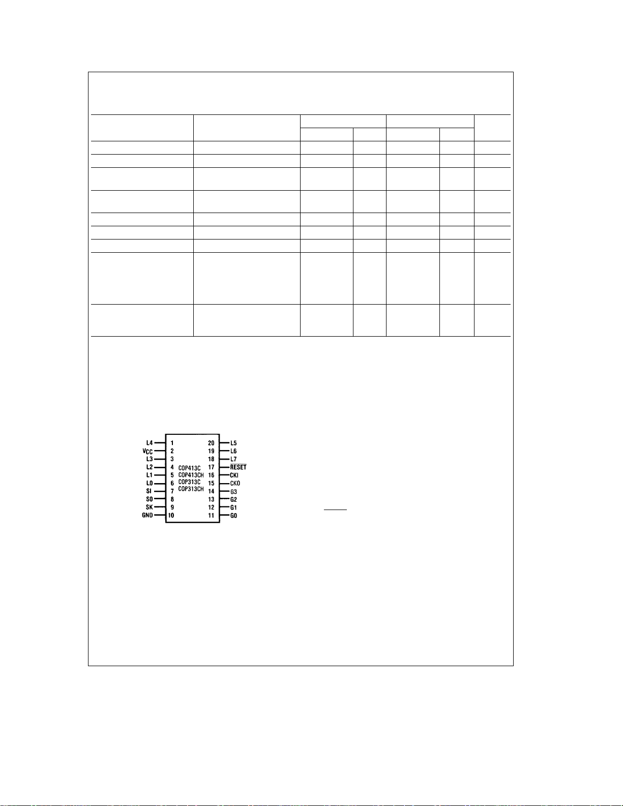
Connection Diagram
DIP
TL/DD/8537– 2
Top View
Order Number COP313C-XXX/D, COP313CH-XXX/D,
COP413C-XXX/D or COP413CH-XXX/D
See NS Hermetic Package Number D20A
Order Number COP313C-XXX/N, COP313CH-XXX/N,
COP413C-XXX/N or COP413CH-XXX/N
See NS Molded Package Number N20A
Order Number COP313C-XXX/WM or
COP413C-XXX/WM
See NS Small Outline Package Number M20B
Pin Descriptions
Pin Description
L
7–L0
G
3–G0
SI Serial input (or counter input)
SO Serial output (or general purpose output)
SK Logic-controlled clock
CKI System oscillator input
CKO Crystal oscillator output, or NC
RESET
V
CC
GND System Ground
FIGURE 2
5
8-bit bidirectional I/O port with TRI-STATE
4-bit bidirectional I/O port
(or general purpose output)
System reset input
System power supply
 Loading...