


PCI-6110E

PCI-6110E/6111E
User Manual
Multifunction I/O Boards for
PCI Bus Computers
April 1998 Edition
Part Number 321759B-01
© Copyright 1998 National Instruments Corporation. All rights reserved.

Internet Support
E-mail: support@natinst.com
FTP Site: ftp.natinst.com
Web Address: http://www.natinst.com
Bulletin Board Support
BBS United States: 512 794 5422
BBS United Kingdom: 01635 551422
BBS France: 01 48 65 15 59
Fax-on-Demand Support
512 418 1111
Telephone Support (USA)
Tel: 512 795 8248
Fax: 512 794 5678
International Offices
Australia 03 9879 5166, Austria 0662 45 79 90 0, Belgium 02 757 00 20, Brazil 011 288 3336,
Canada (Ontario) 905 785 0085, Canada (Québec) 514 694 8521, Denmark 45 76 26 00,
Finland 09 725 725 11, France 01 48 14 24 24, Germany 089 741 31 30, Hong Kong 2645 3186,
Israel 03 6120092, Italy 02 413091, Japan 03 5472 2970, Korea 02 596 7456, Mexico 5 520 2635,
Netherlands 0348 433466, Norway 32 84 84 00, Singapore 2265886, Spain 91 640 0085, Sweden 08 730 49 70,
Switzerland 056 200 51 51, Taiwan 02 377 1200, United Kingdom 01635 523545
National Instruments Corporate Headquarters
6504 Bridge Point Parkway Austin, Texas 78730-5039 USA Tel: 512 794 0100

Important Information
Warranty
The PCI-6110E/6111E boards are warranted against defects in materials and workmanship for a period of one year
from the date of shipment, as evidenced by receipts or other documentation. National Instruments will, at its option,
repair or replace equipment that proves to be defective during the warranty period. This warranty includes parts and
labor.
The media on which you receive National Instruments software are warranted not to fail to execute programming
instructions, due to defects in materials and workm anship, f or a period of 90 days fr om date of ship ment, as evid enced
by receipts or other documentation. National Instruments will, at its option, repair or replace software media that do
not execute programming instructions if National Instruments receives notice of such defects during the warranty
period. National Instruments does not warrant that the operation of the software shall be uninterrupted or error free.
A Return Material Authorization (RMA) number must be obtained from the factory and clearly marked on the outside
of the package before any equipment will be accepted for warranty work. National Instruments will pay the shipping
costs of returning to the owner p arts whic h are co vered by w arran ty.
National Instruments believes that the information in this manual is accurate. The document has been carefully
reviewed for technical accuracy. In the event that technical or typographical errors exist, National Instruments reserves
the right to make changes to subsequent editions of this document without prior notice to holders of this edition. The
reader should consult National Instruments if errors are suspected. In no event shall National Instrum ents be liable for
any damages arising out of or related to this document or the information contained in it.
E
XCEPT
AS
SPECIFIED
HEREIN
, N
ATIONAL
I
NSTRUMENTS
MAKES
NO
WARRANTIES
,
EXPRESS
OR
IMPLIED
,
AND
SPECIFICALLY
DISCLAIMS
ANY
WARRANTY
OF
MERCHANTABILITY
OR
FITNESS
FOR
A
PARTICULAR
PURPOSE
.
C
USTOMER
’
S
RIGHT
TO
RECOVER
DAMAGES
CAUSED
BY
FAULT
OR
NEGLIGENCE
ON
THE
PART
OF
N
ATIONAL
I
NSTRUMENTS
SHALL
BE
LIMITED
TO
THE
AMOUNT
THERETOFORE
PAID
BY
THE
CUSTOMER
. N
ATIONAL
I
NSTRUMENTS
WILL
NOT
BE
LIABLE
FOR
DAMAGES
RESULTING
FROM
LOSS
OF
DATA
,
PROFITS
,
USE
OF
PRODUCTS
,
OR
INCIDENTAL
OR
CONSEQUENTIAL
DAMAGES
,
EVEN
IF
ADVISED
OF
THE
POSSIBILITY
THEREOF
. This limitation of the liability of National
Instruments will apply regardless of the form of action, whether in contract or tort, including negligence. Any action
against National Instruments must be brought within one year after the cause of action accrues. National Instruments
shall not be liable for any delay in performance due to causes beyond its reasonable control. The warranty provided
herein does not cover damages, defects, malfunctions, or service failures caused by owner’s failure to follow the
National Instruments installation, operation, or maintenance instructions; owner’s modification of the product;
owner’s abuse, misuse, or negligent acts; and power failure or surges, fire, flood, accident, actions of third parties,
or other events outside reasonable control.
Copyright
Under the copyright laws, this publ ication may not be r eproduced or tr ansmitted in any form, electron ic or mechanical,
including photocopying, recording, storing in an information retrieval system, or translating, in whole or in part,
without the prior written consent of National Instruments Corporation.
Trademarks
ComponentWorks™, CVI™, DAQ-STC™, LabVIEW™, Measure™, MITE™, NI-DAQ™, NI-PGIA™, RTSI™,
SCXI™, and VirtualBench™ are trademarks of National Instruments Corporation.
Product and company names listed are trademarks or trade names of their respective companies.
WARNING REGARDING MEDICAL AND CLINICAL USE OF NATIONAL INSTRUMENTS PRODUCTS
National Instruments products are not designed with components and testing intended to ensure a level of reliability
suitable for use in treatment and diagnosis of humans. Applications of National Instruments products involving
medical or clinical treatment can create a potential for accidental injury caused by product failure, or by errors on the
part of the user or application designer. Any use or application of National Instruments products for or involving
medical or clinical treatment must be performed by properly trained and qualified medical personnel, and al l traditional
medical safeguards, equipment, and procedures that are appropriate in the particular situation to prevent serious injury
or death should always continue to be used when National Instruments products are being used. National Instruments
products are NOT intended to be a substitute for any form of esta blishe d process, proced ure, or equipm ent used to
monitor or safeguard human health and safety in medical or clinical treatment.

©
National Instruments Corporation v PCI-6110E/6111E User Manual
Table
of
Contents
About This Manual
Organization of This Manual........................................................................................xi
Conventions Used in This Manual................................................................................xii
National Instruments Documentation.... .................................. .....................................xiii
Related Documentation........................................... ......................................................xiv
Customer Communication. .................................. .........................................................xiv
Chapter 1
Introduction
About the 611
X
E Boards .............................................................................................1-1
What You Need to Get Started.....................................................................................1-2
Software Programming Choices...................................................................................1-2
National Instruments Application Software................................................... 1-2
NI-DAQ Driver Software...............................................................................1-3
Register-Level Programming ................ .........................................................1-4
Optional Equipment....................................... .................................. .............................1-5
Custom Cabling ............................................................................................................1-5
Unpacking.....................................................................................................................1-6
Chapter 2
Installation and Configuration
Software Installation.....................................................................................................2-1
Hardware Installation....................................................................................................2-1
Board Configuration ..................................................................................................... 2-2
Chapter 3
Hardware Overview
Analog Input .................................................................................................................3-2
Input Mode .....................................................................................................3-2
Input Polarity and Input Range.......................................................................3-3
Considerations for Selecting Input Ranges......................................3-4
Input Coupling................................................................................................3-4
Dither..............................................................................................................3-4

Table of Contents
PCI-6110E/6111E User Manual vi
©
National Instruments Corporation
Analog Output.............................................................................................................. 3-5
Analog Trigger .............................................................................................................3-6
Digital I/O............................................... .................................. ....................................3-10
Timing Signal Routing.................................................................................................3-11
Programmable Function Inputs...................................................................... 3-12
Board and RTSI Clocks .................................................................................3-12
RTSI Triggers ....................................................................... .........................3-13
Chapter 4
Signal Connections
I/O Connector...............................................................................................................4-1
I/O Connector Signal Descriptions................................................................4-3
Analog Input Signal Connections................................................................................. 4-8
Types of Signal Sources............................................................................................... 4-9
Floating Signal Sources ................................................................................. 4-9
Ground-Referenced Signal Sources...............................................................4-9
Differential Measurements........................................................................................... 4-9
Differential Connection Considerations......................................................... 4-10
Differential Connections for Ground-Referenced
Signal Sources ............................................................................ ..4-11
Differential Connections for Nonreferenced
or Floating Signal Sources...........................................................4-11
Common-Mode Signal Rejection Considerations..........................................4-12
Analog Output Signal Connections.............................................................................. 4-13
Digital I/O Signal Connections ....................................................................................4-13
Power Connections....................................................................................................... 4-15
Timing Connections .....................................................................................................4-15
Programmable Function Input Connections ..................................................4-16
DAQ Timing Connections............................................................................. 4-17
SCANCLK Signal ........................................................................... 4-18
EXTSTROBE* Signal.....................................................................4-18
TRIG1 Signal....................................................... ............................4-19
TRIG2 Signal....................................................... ............................4-20
STARTSCAN Signal.................................................... ...................4-22
CONVERT* Signal..................................... .................................. ..4-23
AIGATE Signal... .................................. .................................. ........ 4-25
SISOURCE Signal...........................................................................4-25
Waveform Generation Timing Connections..................................................4-26
WFTRIG Signal...............................................................................4-26
UPDATE* Signal ............................................................................4-27
UISOURCE Signal.................................................... ... ...................4-28

Table of Contents
©
National Instruments Corporation vii PCI-6110E/6111E User Manual
General-Purpose Timing Signal Connections................................................4-29
GPCTR0_SOURCE Signal............................................................. .4-29
GPCTR0_GATE Signal...................................................................4-30
GPCTR0_OUT Signal ....................... .................................. ............4-31
GPCTR0_UP_DOWN Signal.............................................. ... .........4-31
GPCTR1_SOURCE Signal............................................................. .4-32
GPCTR1_GATE Signal...................................................................4-32
GPCTR1_OUT Signal ....................... .................................. ............4-33
GPCTR1_UP_DOWN Signal.............................................. ... .........4-34
FREQ_OUT Signal..........................................................................4-35
Field Wiring Considerations.........................................................................................4-35
Chapter 5
Calibration
Loading Calibration Constants .....................................................................................5-1
Self-Calibration.............................................................................................................5-2
External Calibration......................................................................................................5-2
Appendix A
Specifications
Appendix B
Cable Connector Descriptions
Appendix C
Common Questions
Appendix D
Customer Communication
Glossary
Index

Table of Contents
PCI-6110E/6111E User Manual viii
©
National Instruments Corporation
Figures
Figure 1-1. The Relationship between the Programming Environment,
NI-DAQ, and Your Hardware ................ .................................. ............. 1-4
Figure 3-1. PCI-6110E Block Diagram ................................................................... 3-1
Figure 3-2. PCI-6111E Block Diagram ................................................................... 3-2
Figure 3-3. Effects of Dither on Signal Acquisition ................................................ 3-5
Figure 3-4. Analog Trigger Block Diagram for the PCI-6110E.............................. 3-6
Figure 3-5. Analog Trigger Block Diagram for the PCI-6111E.............................. 3-7
Figure 3-6. Below-Low-Level Analog Triggering Mode ........................................3-7
Figure 3-7. Above-High-Level Analog Triggering Mode ....................................... 3-8
Figure 3-8. Inside-Region Analog Triggering Mode............................................... 3-8
Figure 3-9. High-Hysteresis Analog Triggering Mode............................................ 3-9
Figure 3-10. Low-Hysteresis Analog Triggering Mode ............................................3-9
Figure 3-11. CONVERT* Signal Routing.................................................................3-11
Figure 3-12. RTSI Bus Signal Connection ................................................................ 3-13
Figure 4-1. I/O Connector Pin Assignment for the 611
X
E Board ..........................4-2
Figure 4-2. 611
X
E Board PGIA..............................................................................4-8
Figure 4-3. Differential Input Connections for Ground-Referenced Signals........... 4-11
Figure 4-4. Differential Input Connections for Nonreferenced Signals................... 4-12
Figure 4-5. Analog Output Connections..................................................................4-13
Figure 4-6. Digital I/O Connections.........................................................................4-14
Figure 4-7. Timing I/O Connections........................................................................4-16
Figure 4-8. Typical Posttriggered Acquisition.........................................................4-17
Figure 4-9. Typical Pretriggered Acquisition ................................. .........................4-18
Figure 4-10. SCANCLK Signal Timing ....................................................................4-18
Figure 4-11. EXTSTROBE* Signal Timing.............................................................. 4-19
Figure 4-12. TRIG1 Input Signal Timing.................................................................. 4-20
Figure 4-13. TRIG1 Output Signal Timing................................................................ 4-20
Figure 4-14. TRIG2 Input Signal Timing.................................................................. 4-21
Figure 4-15. TRIG2 Output Signal Timing................................................................ 4-21
Figure 4-16. STARTSCAN Input Signal Timing...................................................... 4-22
Figure 4-17. STARTSCAN Output Signal Timing....................................................4-23
Figure 4-18. CONVERT* Input Signal Timing.........................................................4-24
Figure 4-19. CONVERT* Output Signal Timing......................................................4-24
Figure 4-20. SISOURCE Signal Timing....................................................................4-26
Figure 4-21. WFTRIG Input Signal Timing..............................................................4-27
Figure 4-22. WFTRIG Output Signal Timing............................................................4-27
Figure 4-23. UPDATE* Input Signal Timing ............................................................4-28
Figure 4-24. UPDATE* Output Signal Timing.........................................................4-28
Figure 4-25. UISOURCE Signal Timing...................................................................4-29
Figure 4-26. GPCTR0_SOURCE Signal Timing ...................................................... 4-30

Table of Contents
©
National Instruments Corporation ix PCI-6110E/6111E User Manual
Figure 4-27. GPCTR0_GATE Signal Timing in Edge-Detection Mode ...................4-31
Figure 4-28. GPCTR0_OUT Signal Timing ..............................................................4-31
Figure 4-29. GPCTR1_SOURCE Signal Timing.......................................................4-32
Figure 4-30. GPCTR1_GATE Signal Timing in Edge-Detection Mode ...................4-33
Figure 4-31. GPCTR1_OUT Signal Timing ..............................................................4-33
Figure 4-32. GPCTR Timing Summary.....................................................................4-34
Figure B-1. 68-Pin 611
X
E Series Connector Pin Assignments ...............................B-2
Tables
Table 3-1. Actual Range and Measurement Precision............................................3-3
Table 4-1. Signal Descriptions for I/O Connector Pins .........................................4-3
Table 4-2. I/O Signal Summary for the 611
X
E ..................................................... 4-6
Table 4-3. Signal Source Types ..............................................................................4-10

©
National Instruments Corporation xi PCI-6110E/6111E User Manual
About
This
Manual
This manual describes the electrical and mechanical aspects of the
611
X
E family of boards and contains information concerning their
operation and programming.
The 611
X
E family of boards includes:
• PCI-6110E
• PCI-6111E
Your 611
X
E board is a high-performance multifunction analog, digital,
and timing I/O board for PCI bus computers. Supported functions
include analog input, analog output, digital I/O, and timingI/O.
Organization of This Manual
The
PCI-6110E/6111E User Manual
is organized as follows:
• Chapter1,
Introduction
, describes your 611
X
E board, lists what
you need to get started, describes the optional software and optiona l
equipment, and explains how to unpack your 611
X
E board.
• Chapter2,
Installation and Configuration
, explains how to install
and configure your 611
X
E board.
• Chapter3,
Hardware Overview
, presents an overview of the
hardware functions on your 611
X
E board.
• Chapter4,
Signal Connections
, describes how to make input and
output signal connections to your 611
X
E
board via the board I/O
connector.
• Chapter5,
Calibration
, discusses the
calibration procedures for
your 611
X
E board.
• AppendixA,
Specifications
, lists the specifications of your 611
X
E
board.
• AppendixB,
Cable Connector Descriptions
, describes the cable
connectors on your 611
X
E board.

About This Manual
PCI-6110E/6111E User Manual xii
©
National Instruments Corporation
• AppendixC,
Common Questions
, contains a list of commonly
asked questions and their answers relating to usage and special
features of your 611
X
E
board.
• AppendixD,
Customer Communication
, contains forms you can
use to request help from National Instruments or to comment on
ourproducts.
•The
Glossary
contains an alphabetical list and description of terms
used in this manual, including acronyms, abbreviations, defini tions
metric prefixes, mnemonics, and symbols.
•The
Index
alphabetically lists topics covered in this manual,
including the page where you can find the topic.
Conventions Used in This Manual
The following conventions are used in this manual.
<> Angle brackets enclose the name of a key on the keyboard (for example,
<option>). Angle brackets containing numbers separated by an ellipsis
represent a range of values associated with a bit or signal name
(forexample, DIO<3..0>).
611
X
E This refers to either the PCI-6110E or PCI-6111E board.
This icon to the left of bold italiciz ed text de notes a n ote, which al erts
you to important information.
This icon to the left of bold italiciz ed text de notes a ca ution, wh ich
advises you of precautions to take to avoid injury, data los s, or a
systemcrash.
bold Bold text denotes the names of menus, menu items, parameters, dialog
boxes, dialog box buttons or options, icons, windows, Win dows 95 tabs,
or LEDs.
bold italic Bold italic text denotes a note, caution, or warning.
italic
Italic text denotes emphasis, a cross reference, or an introduction to a
key concept. This font also denotes text from which you supply the
appropriate word or value, as in Windows 3.
x
.
Macintosh Macintosh refers to all Macintosh OS computers with PCI bus, unless
otherwise noted.
!

About This Manual
©
National Instruments Corporation xiii PCI-6110E/6111E User Manual
monospace Text in this font denotes text or characters that you should literally enter
from the keyboard, sections of code, programming examples, and
syntax examples. This font also is used for the proper names of disk
drives, paths, directories, programs, subprograms, subroutines, device
names, functions, operations, variables, filenames, and extensions, and
for statements and comments taken from program code.
NI-DAQ NI-DAQ refers to the NI-DAQ driver software for Macintosh or
PC compatible computers unless otherwise noted.
PC Refers to all PC AT series computers with PCI bus unless otherwise
noted.
SCXI SCXI stands for Signal Conditioning eXentsions for Instrumentation
and is a National Instruments product line designed to perform
front-end signal conditioning for National instruments plug-in DAQ
boards.
National Instruments Documentation
The
PCI-6110E/6111E User Manual
is one piece of the documentation
set for your DAQ system. You could have any of several types of
documentation depending on the hardware and software in your system.
Use the documentation you have as follows:
•
Getting Started with SCXI
—If you are using SCXI, this is the first
manual you should read. It gives an overview of the SCXI system
and contains the most commonly needed information for the
modules, chassis, and software.
• Your SCXI hardware user manuals—If you are using SCXI, read
these manuals next for detailed information about signal
connections and module configuration. They also explai n in greater
detail how the module works and contain application hints.
• Your DAQ hardware documentation—This documentation has
detailed information about the DAQ h ardware that plugs in to or is
connected to your computer. Use this documentation for hardware
installation and configuration instructions, specification
information about your DAQ hardware, and application hints.
• Software documentation—You may have both application software
and NI-DAQ software documentation. National Instruments
application software includes ComponentWorks, LabVIEW,
LabWindows/CVI, Measure, and VirtualBench. After you set up
your hardware system, use either your application software

About This Manual
PCI-6110E/6111E User Manual xiv
©
National Instruments Corporation
documentation or the NI-DAQ documentation to help you write
your application. If you have a large, complicated system, it is
worthwhile to look through the software documentation before you
configure your hardware.
• Accessory installation guides or manuals—If you are using
accessory products, read the terminal block and cable assembly
installation guides. They explain how to physically connect the
relevant pieces of the system. Consult these guides when you are
making your connections.
• SCXI chassis manuals—If you are using SCXI, read these manuals
for maintenance information on the chassis and installation
instructions.
Related Documentation
The following documents contain information you may find helpful:
• DAQ-STC Technical Reference Manual
• National Instruments Application Note 025,
Field Wiring and Noise
Considerations for Analog Signals
• PCI Local Bus Specification Revision 2.0
Customer Communication
National Instruments wants to receive your comments on our products
and manuals. We are interested in the applications you develop with our
products, and we want to help if you have problems with them. To make
it easy for you to contact us, this manual contains comment and
configuration forms for you to complete. These forms are in
AppendixD,
Customer Communication
, at the end of this manual.

©
National Instruments Corporation 1-1 PCI-6110E/6111E User Manual
Chapter
1
Introduction
This chapter describes your 611
X
E board, lists what you need to get
started, describes the optional software and optional equipment, and
explains how to unpack your 611
X
E board.
About the 611
X
E Boards
Thank you for buying a National Instruments PCI-6110E/6111E
board. Your 611
X
E board is a completely Plug and Play, multifunction
analog, digital, and timing I/O board for PCI bus computers. The
611
X
E board features a 12-bit ADC per channel with four or two
simultaneously sampling analog inputs, 16-bit DACs with voltage
outputs, eight lines of TTL-compatible digital I/O, and two 24-bit
counter/timers for timing I/O. Because the 611
X
E board has no DIP
switches, jumpers, or potentiometers, it is easily software-configured
and calibrated.
The 611
X
E board is a completely switchless and jumperless data
acquisition (DAQ) board for the PCI bus. This feature is made possible
by the National Instruments MITE bus interface chip that connects the
board to the PCI I/O bus. The MITE implements the PCI Local Bus
Specification so that the interrupts and base memory addresses are all
software configured.
The 611
X
E board uses the National Instruments DAQ-STC system
timing controller for time-related functions. The DAQ-STC consists
of three timing groups that control analog input, analog output, and
general-purpose counter/timer functions. These groups include a total
of seven 24-bit and three 16-bit counters and a maximum timing
resolution of 50 ns. The DAQ-STC makes possible such applications as
buffered pulse generation, equivalent time sampling, and seamlessly
changing the sampling rate.
Often with DAQ boards, you cannot easily synchronize several
measurement functions to a common trigger or timing event. The
611
X
E board has the Real-Time System Integration (RTSI) bus to
solve this problem. The RTSI bus consists of our RTSI bus interface

Chapter 1 Introduction
PCI-6110E/6111E User Manual 1-2
©
National Instruments Corporation
and a ribbon cable to route timing and trigger signals between several
functions on as many as five DAQ boards in your computer.
Detailed specifications of the 611
X
E board are in Appendix A,
Specifications
.
What You Need to Get Started
To set up and use the 611
X
E board, you will need the following:
❑ Either the PCI-6110E or PCI-6111E board
❑
PCI-6110E/6111E User Manual
❑ One of the following software packages and documentation:
ComponentWorks
LabVIEW for Macintosh
LabVIEW for Windows
LabWindows/CVI for Windows
Measure
NI-DAQ for PC Compatibles
VirtualBench
❑ Your computer
Software Programming Choices
You have several options to choose from when programming your
National Instruments DAQ and SCXI hardware. You can use National
Instruments application software, NI-DAQ, or register-level
programming.
National Instruments Application Software
ComponentWorks contains tools for data acquisition and instrument
control built on NI-DAQ driver software. ComponentWorks provides
a higher-level programming interface for building virtual instruments
through standard OLE controls and DLLs. With Compon entWorks, you
can use all of the configuration tools, resource management utilities,
and interactive control utilities included with NI-DAQ.
LabVIEW features interactive graphics, a state-of-the-art user
interface, and a powerful graphical programming language. The

Chapter 1 Introduction
©
National Instruments Corporation 1-3 PCI-6110E/6111E User Manual
LabVIEW Data Acquisition VI Library, a series of VIs for using
LabVIEW with National Instruments DAQ hardware, is included with
LabVIEW. The LabVIEW Data Acquisition VI Library is functionally
equivalent to NI-DAQ software.
LabWindows/CVI features interactive graphics, state-of-the-art user
interface, and uses the ANSI standard C programming language. The
LabWindows/CVI Data Acquisition Library, a series of functions for
using LabWindows/CVI with National Instruments DAQ hardware, is
included with the NI-DAQ software kit. The LabWindows/CVI Data
Acquisition Library is functionally equivalent to the NI-DAQ softwar e.
VirtualBench features virtual instruments that combine DAQ pr oduct s,
software, and your computer to create a stand-alone instrument with the
added benefit of the processing, display, and storage cap abilities of
your computer. VirtualBench instruments load and save waveform data
to disk in the same forms that can be used in popular spreadsheet
programs and word processors.
Using ComponentWorks, LabVIEW, LabWindows/CVI, or
VirtualBench software will greatly reduce the development time
for your data acquisition and control application.
NI-DAQ Driver Software
The NI-DAQ driver software is included at no charge with all National
Instruments DAQ hardware. NI-DAQ is not packaged with SCXI or
accessory products, except for the SCXI-1200. NI-DAQ has an
extensive library of functions that you can call from your application
programming environment. These functions include routi nes for analog
input (A/D conversion), buffered data acquisition (high-speed A/D
conversion), analog output (D/A conversion), waveform generation
(timed D/A conversion), digital I/O, counter/timer operations, SCXI,
RTSI, self-calibration, messaging, and acquiring data to extended
memory.
NI-DAQ has both high-level DAQ I/O functions for maximum ease of
use and low-level DAQ I/O functions for maximum flexibility and
performance. Examples of high-level functions are streaming data to
disk or acquiring a certain number of data points. An example of a
low-level function is writing directly to registers on the DAQ device.
NI-DAQ does not sacrifice the performance of National Instruments
DAQ devices because it lets multiple devices operate at their peak.
Chapter 1 Introduction
PCI-6110E/6111E User Manual 1-4
©
National Instruments Corporation
NI-DAQ also internally addresses many of the complex issues between
the computer and the DAQ hardware such as programming interrupts
and DMA controllers. NI-DAQ maintains a consistent software
interface among its different versions so that you can change platfor ms
with minimal modifications to your code. Whether you are using
conventional programming languages or National Instruments
application software, your application uses the NI-DAQ driver
software, as illustrated in Figure 1-1.
Figure 1-1. The Relationship between the Programming Environment,
NI-DAQ, and Your Hardware
Register-Level Programming
The final option for programming any National Instruments DAQ
hardware is to write register-level software. Writing register-level
programming software can be very time-consuming and inefficient,
and is not recommended for most users.
Even if you are an experienced register-level programmer, using
NI-DAQ or application software to program your National Instruments
DAQ hardware is easier than, and as flexible as, register-level
programming, and can save weeks of development time.
NI-DAQ
Driver Software
DAQ or
SCXI Hardware
Personal Computer
or Workstation
Conventional
Programming
Environment
ComponentWorks,
LabVIEW,
LabWindows/CVI,
or VirtualBench

Chapter 1 Introduction
©
National Instruments Corporation 1-5 PCI-6110E/6111E User Manual
Optional Equipment
National Instruments offers a variety of produ cts to use with the 611
X
E
board, including cables, connector blocks, and other accessories, as
follows:
• Cables and cable assemblies
• Connector blocks, shielded and unshielded 50- and 68-pin screw
terminals
• RTSI bus cables
• Low channel-count signal conditioning modules, boards, and
accessories, including conditioning for strain gauges, RTDs,
and relays
For more specific information about these products, refer to your
National Instruments catalogue or call the office nearest you.
Custom Cabling
National Instruments offers cables and accessories for you to prototype
your application or to use if you frequently change board
interconnections.
If you want to develop your own cable, however, the following
guidelines may be useful:
• For the analog input signals, shielded twisted-pair wires for each
analog input pair yield the best results, assuming that you use
differential inputs. Tie the shield for each signal pair to the ground
reference at the source.
• Route the analog lines separately from the digital lines.
• When using a cable shield, use separate shields for the analog and
digital halves of the cable. Failure to do so results in noise coupling
into the analog signals from transient digital signals.
Mating connectors and a backshell kit for making custom 68-pin cables
are available from National Instruments.

Chapter 1 Introduction
PCI-6110E/6111E User Manual 1-6
©
National Instruments Corporation
The following list gives recommended part numbers for connectors that
mate to the I/O connector on the 611
X
E
board:
• Honda 68-position, solder cup, female connector
(part number PCS-E68FS)
• Honda backshell (part number PCS-E68LKPA)
Unpacking
The 611
X
E board is shipped in an antistatic package to prevent
electrostatic damage to the board. Electrostatic discharge can damage
several components on the board. To avoid such damage in handling
the board, take the following precautions:
• Ground yourself via a grounding strap or by holding a grounded
object.
• Touch the antistatic package to a metal part of your computer
chassis before removing the board from the package.
• Remove the board from the package and inspect the board for
loose components or any other sign of damage. Notify National
Instruments if the board appears damaged in any way. Do
not
install a damaged board into your computer.
•
Never
touch the exposed pins of connectors.

©
National Instruments Corporation 2-1 PCI-6110E/6111E User Manual
Chapter
2
Installation and
Configuration
This chapter explains how to install and configure your 611
X
E board.
Software Installation
Install your software before you install the 611
X
E board. Refer to the
appropriate release notes indicated below for specific instructions on
the software installation sequence.
If you are using LabVIEW, LabWindows/CVI, or other National
Instruments application software packages, refer to the appropriate
release notes. After you have installed your application software, refer
to your NI-DAQ release notes and follow the instructions given there
for your operating system and application software package.
If you are using NI-DAQ, refer to your NI-DAQ release notes. Find
theinstallation section for your operating system and follow the
instructions given there.
Hardware Installation
You can install the 611
X
E board in any available expansion slot in your
computer. However, to achieve best noise performance, leave as much
room as possible between the 611
X
E board and other boards and
hardware. The following are general installation instructions, but
consult your computer user manual or technical reference manual for
specific instructions and warnings.
1. Write down the 611
X
E board serial number in the
PCI-6110E/6111E Hardware and Software Configuration Form
in
AppendixD,
Customer Communication
, of this manual.
2. Turn off and unplug your computer.
3. Remove the top cover or access port to the I/O channel.
4. Remove the expansion slot cover on the back panel of the
computer.

Chapter 2 Installation and Configuration
PCI-6110E/6111E User Manual 2-2
©
National Instruments Corporation
5. Insert the 611
X
E board into a 5 V PCI slot. Gently rock the board
to ease it into place. It may be a tight fit, but
do not force
the board
into place.
6. If required, screw the mounting bracket of the 611
X
E board to the
back panel rail of the computer.
7. Replace the cover.
8. Plug in and turn on your computer.
The 611
X
E board is installed. You are now ready to configure your
software. Refer to your software documentation for configuration
instructions.
Board Configuration
Due to the National Instruments standard architecture for data
acquisition and the PCI bus specification, the 611
X
E board
is completely software configurable. You must perform two types
of configuration on the 611
X
E
board—bus-related and data
acquisition-related configuration.
The 611
X
E board is fully compatible with the industry standard
PCI Local Bus Specification Revision 2.0
. This allows the PCI system to
automatically perform all bus-related configurations and requires no
user interaction. Bus-related configuration includes setting the board
base memory address and interrupt channel.
Data acquisition-related configuration includes such settings as analog
input coupling and range, and others. You can modify these settings
using NI-DAQ or application level software, such as ComponentWorks,
LabVIEW, LabWindows/CVI, and VirtualBench.
©
National Instruments Corporation 3-1 PCI-6110E/6111E User Manual
Chapter
3
Hardware Overview
This chapter presents an overview of the hardware functions on your
611
X
E
board. Figure 3-1 shows a block diagram for the
PCI-6110E board.
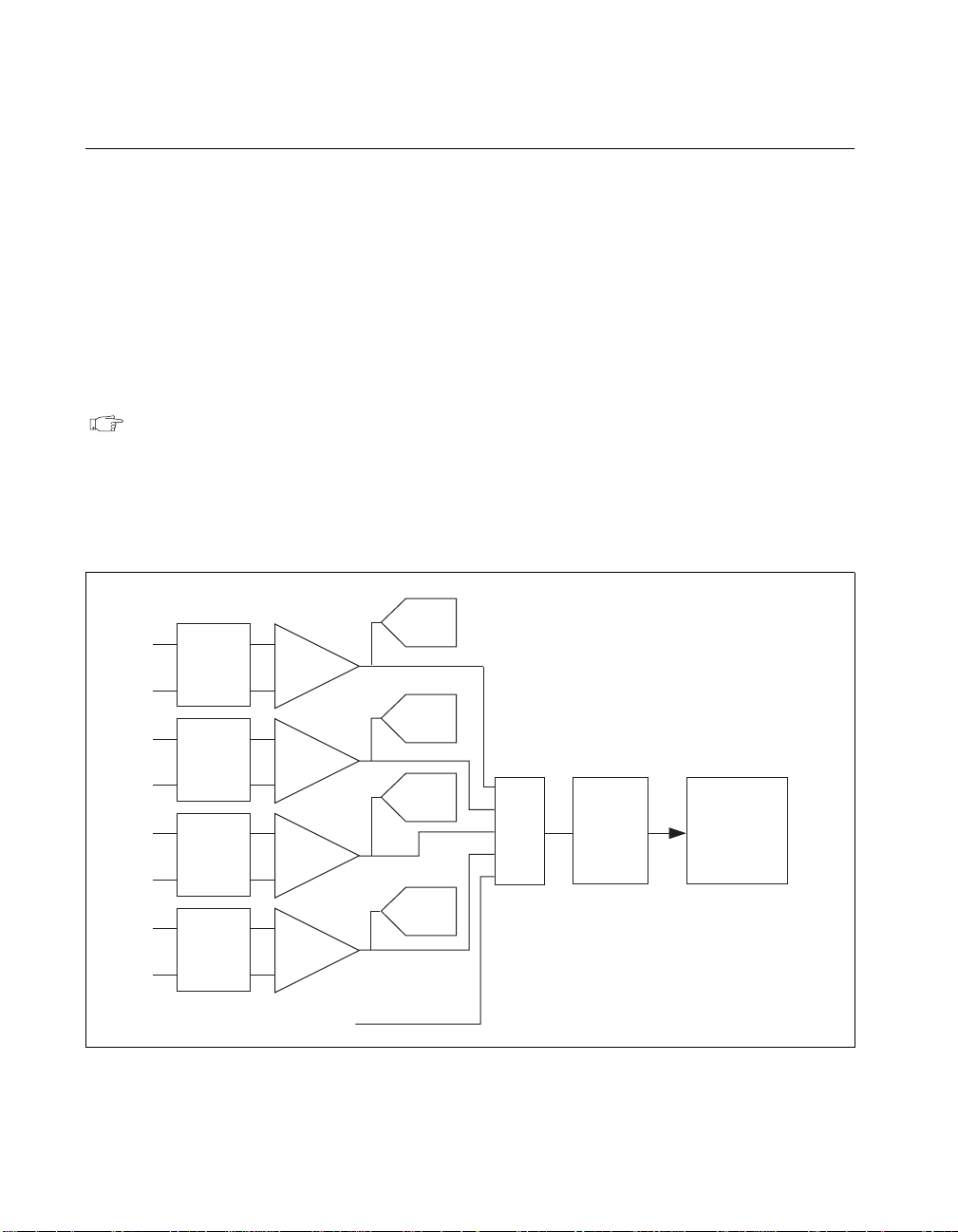
Figure 3-1.
PCI-6110E Block Diagram
Timing
PFI / Trigger
I/O Connector
RTSI Bus
PCI Bus
Digital I/O (8)
EEPROM
+
CH0
Amplifier
–
Calibration
Mux
AI CH0
Mux
CH0
Latch
Analog
Trigger
Circuitry
2
Trigger Level
DACs
Trigger
12
4
Calibration
DACs
DAC0
DAC1
CH0
12-Bit ADC
DAQ - STC
Analog Input
Timing/Control
Analog Output
Timing/Control
Digital I/O
Trigger
Counter/
Timing I/O
RTSI Bus
Interface
DMA/IRQ
Bus
Interface
DAC
FIFO
Data (32)
Address/Data
Control
Data (32)
Analog
Input
Control
EEPROM
Control
DMA
Interface
FPGA
DAQ-STC
Bus
Interface
Analog
Output
Control
I/O
Bus
Interface
Mini
MITE
Generic
Bus
Interface
PCI
Bus
Interface
IRQ
DMA
AO Control
CH0+
CH0-
+
CH1
Amplifier
–
AI CH1
Mux
CH1
Latch
12
CH1
12-Bit ADC
CH1+
CH1-
+
CH2
Amplifier
–
AI CH2
Mux
CH2
Latch
12
CH2
12-Bit ADC
CH2+
CH2-
+
CH3
Amplifier
–
AI CH3
Mux
CH3
Latch
12
CH3
12-Bit ADC
CH3+
CH3-
AI Control
Data (16)
Data (16)
Data (16)
Data (16)
ADC
FIFO
Data (16)
Chapter 3 Hardware Overview
PCI-6110E/6111E User Manual 3-2
©
National Instruments Corporation
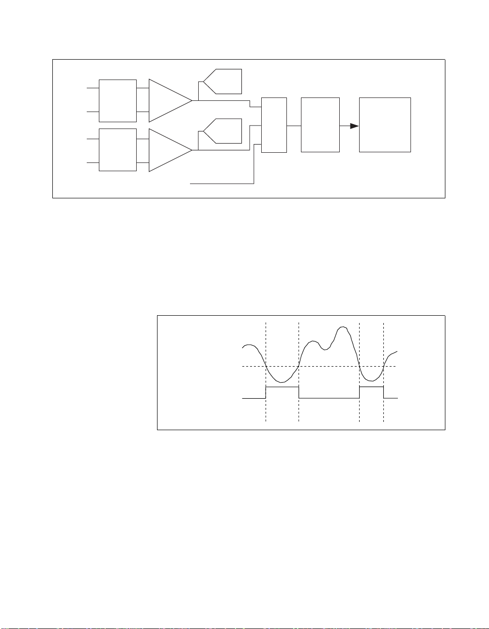
Figure 3-2 shows a block diagram for the PCI-6111E board.
Figure 3-2. PCI-6111E Block Diagram
Analog Input
The analog input section for the 611
X
E
board is software configurable.
You can select different analog input configurations through
application software. The following sections describe in detail each of
the analog input categories.
Input Mode
The 611
X
E board supports only differential inputs (DIFF). The DIFF
input configuration provides up to four channels on the PCI-6110E
board and up to two channels on the PCI-6111E board.
A channel configured in DIFF mode uses two analog channel input lines.
One line connects to the positive input of the board programmable gain
instrumentation amplifier (PGIA), and the other connects to the negative
input of the PGIA. For more information about DIFF input
Timing
PFI / Trigger
I/O Connector
RTSI Bus
PCI Bus
Digital I/O (8)
EEPROM
+
CH0
Amplifier
–
Calibration
Mux
AI CH0
Mux
CH0
Latch
Analog
Trigger
Circuitry
2
Trigger Level
DACs
Trigger
12
4
Calibration
DACs
DAC0
DAC1
CH0
12-Bit ADC
DAQ - STC
Analog Input
Timing/Control
Analog Output
Timing/Control
Digital I/O
Trigger
Counter/
Timing I/O
RTSI Bus
Interface
DMA/IRQ
Bus
Interface
DAC
FIFO
Data (32)
Address/Data
Control
Data (32)
Analog
Input
Control
EEPROM
Control
DMA
Interface
FPGA
DAQ-STC
Bus
Interface
Analog
Output
Control
I/O
Bus
Interface
Mini
MITE
Generic
Bus
Interface
PCI
Bus
Interface
IRQ
DMA
AO Control
CH0+
CH0-
+
CH1
Amplifier
–
AI CH1
Mux
CH1
Latch
12
CH1
12-Bit ADC
CH1+
CH1-
AI Control
Data (16)
Data (16)
ADC
FIFO

Chapter 3 Hardware Overview
©
National Instruments Corporation 3-3 PCI-6110E/6111E User Manual
configuration, refer to the
Analog Input Signal Connections
section in
Chapter4,
Signal Connections
, which contains diagrams showing the
signal paths for DIFF input.
Input Polarity and Input Range
The 611
X
E board has bipolar inputs only. Bipolar input m eans that the
input voltage range is between –V
ref
/2
and + V
ref
/2. These boards have
a bipolar input range of 20V (±10 V).
You can program range settings on a per channel basis so that you can
configure each input channel uniquely.
The software-programmable gain on these boards increases their
overall flexibility by matching the input signal ranges to those that the
ADC can accommodate. They have gains of 0.2, 0.5, 1, 2, 5, 10, 20, and
50, and are suited for a wide variety of signal levels. With the proper
gain setting, you can use the full resolution of the ADC to measure the
input signal. Table3-1 shows the overall input range and precision
according to the gain used.
Table 3-1.
Actual Range and Measurement Precision
Range
Configuration
Gain Actual Input Range
1
Precision
2
–10 to +10 V 0.2
0.5
1.0
2.0
5.0
10.0
20.0
50.0
–50 to +50 V
–20 to +20 V
–10 to +10 V
–5 to +5 V
–2 to +2 V
–1 to +1V
–500 to +500 mV
–200 to +200 mV
24.41 mV
9.77 mV
4.88 mV
2.44 mV
976.56 µV
488.28 µV
244.14 µV
97.66 µV
1
Warning:
The 611
X
E is not designed for input voltages greater than 42 V, even if a
user-installed voltage divider reduces the voltage to within the input range of the DAQ
device. Input voltages greater than 42 V can damage the 611
X
E, any device connected to
it, and the host computer. Overvoltage can also cause an electric shock hazard for the
operator. National Instruments is NOT liable for damage or injury resulting from such
misuse.
2
The value of 1 LSB of the 12-bit ADC; that is, the voltage increment corresponding to a
change of one count in the ADC 12-bit count.
Note:
See Appendix A,
Specifications
, for absolute maximum ratings.

Chapter 3 Hardware Overview
PCI-6110E/6111E User Manual 3-4
©
National Instruments Corporation
Considerations for Selecting Input Ranges
The range you select depends on the expected range of the incoming
signal. A large input range can accommodate a large signal variation
but reduces the voltage resolution. Choosing a smaller input range
improves the voltage resolution but may result in the input signal going
out of range. For best results, match the input range as closely as
possible to the expected range of the input signal.
Input Coupling
You can configure the 611
X
E board for either AC or DC input coupling
on a per channel basis. Use AC coupling when your AC signal contains
a large DC component. If you enable AC coupling, you remove the
large DC offset for the input amplifier and amplify only the AC
component. This makes effective use of the ADC dynamic range.
Dither
Dither adds approximately 0.5 LSBrms of white Gaussian noise to
the signal to be converted by the ADC. This addition is useful for
applications involving averaging to increase the resolution of the
611
X
E board, as in calibration or spectral analysis. In such
applications, noise modulation is decreased and differential linearity is
improved by the addition of the dither. When taking DC measurements,
such as when checking the board calibration, you should average about
1,000 points to take a single reading. This process removes the effects
of quantization and reduces measurement noise, resulting in improved
resolution.
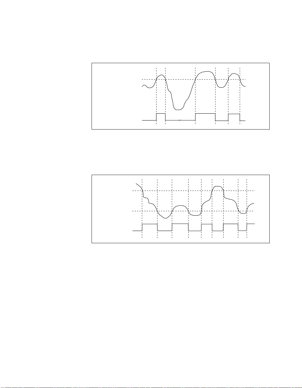
Figure 3-3 illustrates the effect of dither on signal acquisition.
Figure 3-3a shows a small (±4 LSB) sine wave acquired without dither.
The ADC quantization is clearly visible. Figure 3-3b shows what
happens when 50 such acquisitions are averaged together; quantization
is still plainly visible. In Figure 3-3c, the sine wave is acquired with
dither. There is a considerable amount of visible noise. But averaging
about 50 such acquisitions, as shown in Figure 3-3d, eliminates both the
added noise and the effects of quantization. Dither has the effect of
forcing quantization noise to become a zero-mean random variable
rather than a deterministic function of the input signal.
Chapter 3 Hardware Overview
©
National Instruments Corporation 3-5 PCI-6110E/6111E User Manual
You cannot disable dither on the 611
X
E board. This is because the
ADC resolution is so fine that the ADC and the PGIA inherently
produce almost 0.5 LSBrms of noise. This is equivalent to having a
dither circuit that is always enabled.
Figure 3-3. Effects of Dither on Signal Acquisition
Analog Output
The 611
X
E boa r d supplies two channels of analog output voltage at the
I/O connector. The range is fixed at bipolar ±10 V.
a. Dither disabled; no averaging b. Dither disabled; average of 50 acquisitions
c. Dither enabled; no averaging d. Dither enabled; average of 50 acquisitions
LSBs
100 200 300 4000 500
-4.0
-2.0
0.0
2.0
4.0
-6.0
6.0
LSBs
100 200 300 4000 500
-4.0
-2.0
0.0
2.0
4.0
-6.0
6.0
LSBs
100 200 300 4000 500
-4.0
-2.0
0.0
2.0
4.0
-6.0
6.0
LSBs
100 200 300 4000 500
-4.0
-2.0
0.0
2.0
4.0
-6.0
6.0
LSBs
100 200 300 4000 500
-4.0
-2.0
0.0
2.0
4.0
-6.0
6.0
LSBs
100 200 300 4000 500
-4.0
-2.0
0.0
2.0
4.0
-6.0
6.0
100 200 300 4000 500
-4.0
-2.0
0.0
2.0
4.0
-6.0
LSBs
6.0
100 200 300 4000 500
-4.0
-2.0
0.0
2.0
4.0
-6.0
LSBs
6.0
Chapter 3 Hardware Overview
PCI-6110E/6111E User Manual 3-6
©
National Instruments Corporation
Analog Trigger
In addition to supporting internal software triggering and external
digital triggering to initiate a data acquisition sequence, these boards
also support analog triggering. You can configure the analog trigger
circuitry to accept either a direct analog input from the PFI0/TRIG1 pin
on the I/O connector or a postgain signal from the output of the PGIA
on any of the channels, as shown in Figures 3-4 and 3-5. The
trigger-level range for the direct analog channel is ±10 V in 78 mV steps
for the 611
X
E
board. The range for the post-PGIA trigger selection is
simply the full-scale range of the selected channel, and the resolution is
that range divided by 256.
Note: The PFI0/TRIG1 pin is an analog input when configured as an analog
trigger. Therefore, it is susceptible to crosstalk from adjacent pins, which
can result in false triggering when the pin is left unconnected. To avoid
false triggering, make sure this pin is connected to a low-impedance signal
source (less than 1 kΩ source impedance) if you plan to enable this input
via software.
Figure 3-4.
Analog Trigger Block Diagram for the PCI-6110E
PGIA
Analog
Input
CH0
+
-
ADC
ADC
ADC
DAQ-STC
Analog
Trigger
Circuit
Mux
PGIA
Analog
Input
CH1
+
-
PGIA
Analog
Input
CH2
+
-
PGIA
Analog
Input
CH3
+
-
ADC
PFI0/TRIG1
Chapter 3 Hardware Overview
©
National Instruments Corporation 3-7 PCI-6110E/6111E User Manual
Figure 3-5. Analog Trigger Block Diagram for the PCI-6111E
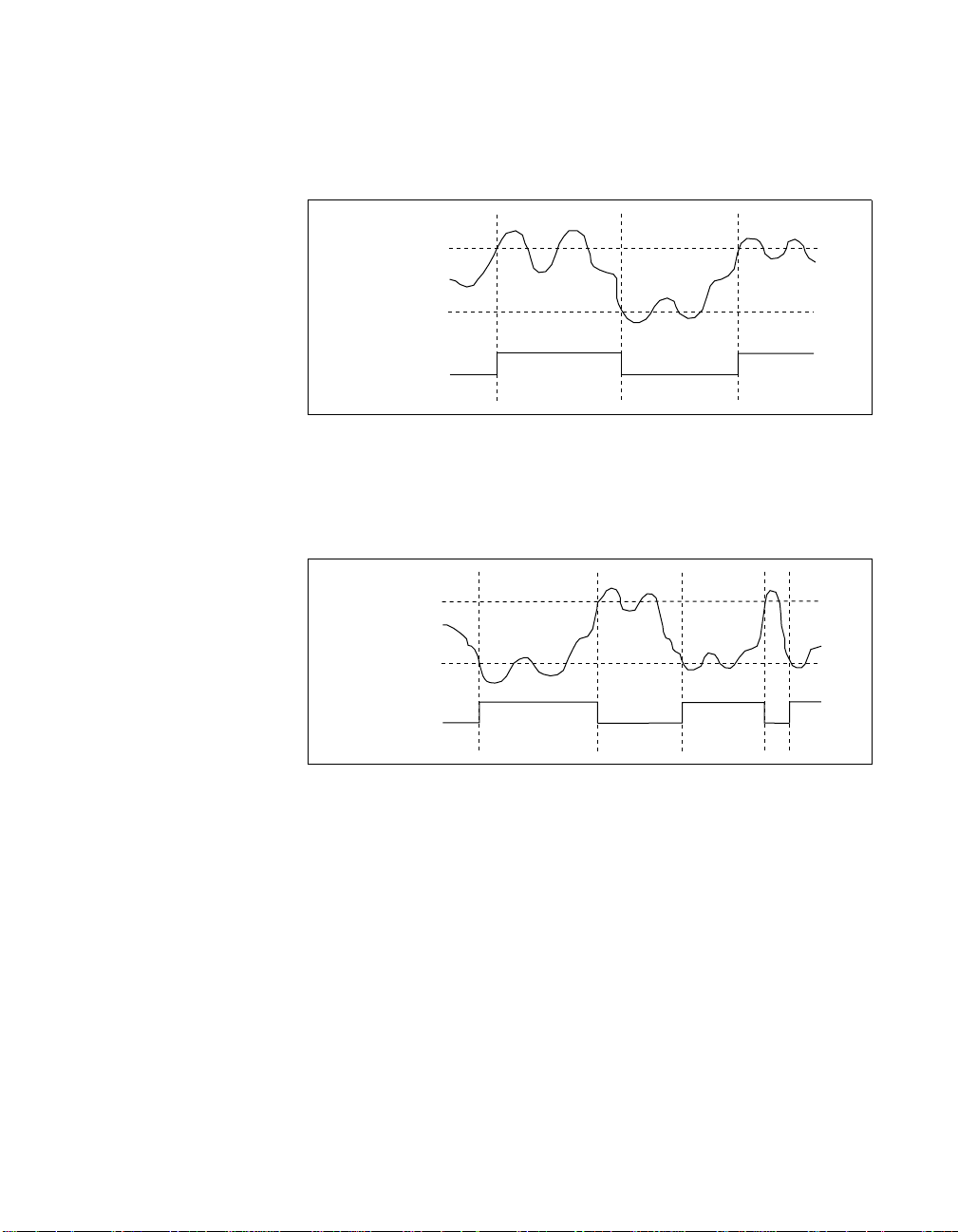
Five analog triggering modes are available, as shown in Figures 3-6
through 3-10. You can set lowValue and highValue independently in
software.
In below-low-level analog triggering mode, the trigger is generated
when the signal value is less than lowValue, as shown in Figure 3-6.
HighValue is unused.
Figure 3-6. Below-Low-Level Analog Triggering Mode
PGIA
Analog
Input
CH0
+
-
ADC
DAQ-STC
Analog
Trigger
Circuit
Mux
PGIA
Analog
Input
CH1
+
-
ADC
PFI0/TRIG1
lowValue
Trigger
Chapter 3 Hardware Overview
PCI-6110E/6111E User Manual 3-8
©
National Instruments Corporation
In above-high-level analog triggering mode, the trigger is generated
when the signal value is greater than highValue, as shown in Figure 3-7.
LowValue is unused.
Figure 3-7. Above-High-Level Analog Triggering Mode
In inside-region analog triggering mode, the trigger is generated when
the signal value is between the lowValue and the highValue, as shown
in Figure 3-8.
Figure 3-8. Inside-Region Analog Triggering Mode
highValue
Trigger
highValue
Trigger
lowValue
Chapter 3 Hardware Overview
©
National Instruments Corporation 3-9 PCI-6110E/6111E User Manual
In high-hysteresis analog triggering mode, the trigger is generated when
the signal value is greater than highValue, with the hysteresis specified
by lowValue, as shown in Figure 3-9.
Figure 3-9. High-Hysteresis Analog Triggering Mode
In low-hysteresis analog triggering mode, the trigger is generated when
the signal value is less than lowValue, with the hysteresis specified by
highValue, as shown in Figure 3-10.
Figure 3-10. Low-Hysteresis Analog Triggering Mode
The analog trigger circuit generates an internal digital trigger based on
the analog input signal and the user-defined trigger levels. This digital
trigger can be used by any of the timing sections of the DAQ-STC,
including the analog input, analog output, and general-purpose
counter/timer sections. For example, the analog input section can be
configured to acquire
n
scans after the analog input signal crosses a
specific threshold. As another example, the analog output section can
be configured to update its outputs whenever the analog input signal
crosses a specific threshold.
highValue
Trigger
lowValue
highValue
Trigger
lowValue

Chapter 3 Hardware Overview
PCI-6110E/6111E User Manual 3-10
©
National Instruments Corporation
Digital I/O
The 611
X
E board contains eight lines of digital I/O for general-purpose
use. You can individually software-configure each line for either input
or output. At system startup and reset, the digital I/O ports are all high
impedance.
The hardware up/down control for general-purpose counters 0 and 1 are
connected onboard to DIO6 and DIO7, respectively. Thus, you can use
DIO6 and DIO7 to control the general-purpose counters. The up/down
control signals are input only and do not affect the operation of the DIO
lines.
 Loading...