


May 5, 2008
ADC101C021/ADC101C027
I2C-Compatible, 10-Bit Analog-to-Digital Converter (ADC) with Alert Function
General Description
The ADC101C021 is a low-power, monolithic, 10-bit, analog-to-digital converter(ADC) that operates from a +2.7 to 5.5V supply. The converter is based on a successive approximation register architecture with an internal track-and-hold circuit that can handle input frequencies up to 11MHz. The ADC101C021 operates from a single supply which also serves as the reference. The device features an I2C-compatible serial interface that operates in all three speed modes, including high speed mode (3.4MHz).
The ADC's Alert feature provides an interrupt that is activated when the analog input violates a programmable upper or lower limit value. The device features an automatic conversion mode, which frees up the controller and I2C interface. In this mode, the ADC continuously monitors the analog input for an "out-of-range" condition and provides an interrupt if the measured voltage goes out-of-range.
The ADC101C021 comes in a small TSOT-6 package with an alert output. The ADC101C027 comes in a small TSOT-6 package with an address selection input. The ADC101C027 provides three pin-selectable addresses. Pin-compatible alternatives are available with additional address options.
Normal power consumption using a +3V or +5V supply is 0.26mW or 0.78mW, respectively. The automatic powerdown feature reduces the power consumption to less than 1µW while not converting. Operation over the industrial temperature range of −40°C to +105°C is guaranteed. Their low power consumption and small packages make this family of ADCs an excellent choice for use in battery operated equipment.
The ADC101C021 and ADC101C027 are part of a family of pin-compatible ADCs that also provide 12 and 8 bit resolution. For 12-bit ADCs see the ADC121C021 and ADC121C027. For 8-bit ADCs see the ADC081C021 and ADC081C027.
Features
■I2C-Compatible 2-wire Interface which supports standard (100kHz), fast (400kHz), and high speed (3.4MHz) modes
■Extended power supply range (+2.7V to +5.5V)
■Up to four pin-selectable chip addresses
■Out-of-range Alert Function
■Automatic Power-down mode while not converting
■Very small 6-pin TSOT packages
■±8kV HBM ESD protection (SDA, SCL)
Key Specifications
■ Resolution |
10 bits; no missing codes |
■ Conversion Time |
1µs (typ) |
■ INL & DNL |
±0.5 LSB (max) |
■ Throughput Rate |
188.9kSPS (max) |
■ Power Consumption (at 22kSPS) |
|
— 3V Supply |
0.26 mW (typ) |
— 5V Supply |
0.78 mW (typ) |
Applications
■System Monitoring
■Peak Detection
■Portable Instruments
■Medical Instruments
■Test Equipment
Pin-Compatible Alternatives
All devices are fully pin and function compatible.
Resolution |
ALERT Output |
ADDR Input |
12-bit |
ADC121C021 |
ADC121C027 |
|
|
|
10-bit |
ADC101C021 |
ADC101C027 |
|
|
|
8-bit |
ADC081C021 |
ADC081C027 |
Connection Diagrams
30052001 |
30052002 |
I2C® is a registered trademark of Phillips Corporation.
Alert with (ADC) Converter Digital-to-Analog Bit-10 Compatible,-C2I ADC101C021/ADC101C027
© 2008 National Semiconductor Corporation |
300520 |
www.national.com |

ADC101C021/ADC101C027
Ordering Information
|
Order Code |
Option |
Package |
Top Mark |
|
ADC101C021CIMK |
Alert pin |
TSOT-6 |
X33C |
|
|
|
|
|
|
ADC101C021CIMKX |
Alert pin |
TSOT-6 Tape-and-Reel |
X33C |
|
|
|
|
|
|
ADC101C027CIMK |
Address pin |
TSOT-6 |
X32C |
|
ADC101C027CIMKX |
Address pin |
TSOT-6 Tape-and-Reel |
X32C |
|
|
|
|
|
|
|
Shipped with the ADC101C021. |
|
|
|
ADC101C021EB |
Also compatible with the |
Evaluation Board |
|
|
ADC101C027 option. |
|
||
|
|
|
|
|
|
|
Please order samples. |
|
|
|
|
|
|
|
Block Diagram |
|
|
|
|
30052003
www.national.com |
2 |
Pin Descriptions
Symbol |
Type |
Equivalent Circuit |
Description |
VA |
Supply |
|
Power and unbufferred reference voltage. VA must be free |
|
of noise and decoupled to GND. |
||
|
|
|
|
GND |
Ground |
|
Ground for all on-chip circuitry. |
|
|
|
|
VIN |
Analog Input |
See Figure 4 |
Analog input. This signal can range from GND to VA. |
|
|
|
Alert output. Can be configured as active high or active |
ALERT |
Digital Output |
|
low. This is an open drain data line that must be pulled to |
|
|
|
the supply (VA) with an external pull-up resistor. |
|
|
|
Serial Clock Input. SCL is used together with SDA to |
|
|
|
control the transfer of data in and out of the device. This is |
SCL |
Digital Input |
|
an open drain data line that must be pulled to the supply |
|
(VA) with an external pull-up resistor. This pin's extended |
||
|
|
|
|
|
|
|
ESD tolerance( 8kV HBM) allows extension of the I2C bus |
|
|
|
across multiple boards without extra ESD protection. |
|
|
|
|
|
|
|
Serial Data bi-directional connection. Data is clocked into |
|
|
|
or out of the internal 16-bit register with SCL. This is an |
SDA |
Digital |
|
open drain data line that must be pulled to the supply |
Input/Output |
|
(VA) with an external pull-up resistor. This pin's extended |
|
|
|
||
|
|
|
ESD tolerance( 8kV HBM) allows extension of the I2C bus |
|
|
|
across multiple boards without extra ESD protection. |
|
|
|
|
ADDR |
Digital Input, |
|
Tri-level Address Selection Input. Sets Bits A0 & A1 of the |
three levels |
|
7-bit slave address. (see Table 1) |
|
|
|
||
|
|
|
|
Package Pinouts
|
VA |
GND |
VIN |
ALERT |
SCL |
SDA |
ADDR |
|
ADC101C021 |
1 |
2 |
3 |
4 |
5 |
6 |
N/A |
|
TSOT-6 |
||||||||
|
|
|
|
|
|
|
||
ADC101C027 |
1 |
2 |
3 |
N/A |
5 |
6 |
4 |
|
TSOT-6 |
||||||||
|
|
|
|
|
|
|
ADC101C021/ADC101C027
3 |
www.national.com |

ADC101C021/ADC101C027
Absolute Maximum Ratings
(Notes 1, 2)
If Military/Aerospace specified devices are required, please contact the National Semiconductor Sales Office/ Distributors for availability and specifications.
Supply Voltage, VA
Voltage on any Analog Input Pin to GND
Voltage on any Digital Input Pin to GND
Input Current at Any Pin (Note 3) Package Input Current (Note 3) Power Dissipation at TA = 25°C
ESD Susceptibility (Note 5)
VA, GND, VIN, ALERT, ADDR pins:
Human Body Model Machine Model
Charged Device Model (CDM) SDA, SCL pins:
Human Body Model Machine Model
Junction Temperature
Storage Temperature
-0.3V to +6.5V
−0.3V to (VA +0.3V)
−0.3V to 6.5V ±15 mA ±20 mA
See (Note 4)
2500V
250V
1250V
8000V
400V
+150°C −65°C to +150°C
Operating Ratings (Notes 1, 2)
Operating Temperature Range |
−40°C ≤ TA ≤ +105°C |
Supply Voltage, VA |
+2.7V to 5.5V |
Analog Input Voltage, VIN |
0V to VA |
Digital Input Voltage (Note 7) |
0V to 5.5V |
Sample Rate |
up to 188.9 kSPS |
Package Thermal Resistances
Package |
θJA |
6-Lead TSOT |
250°C/W |
Soldering process must comply with National Semiconductor's Reflow Temperature Profile specifications. Refer to www.national.com/packaging. (Note 6)
Electrical Characteristics
The following specifications apply for VA = +2.7V to +5.5V, GND = 0V, fSCL up to 3.4MHz, fIN = 1kHz for fSCL up to 400kHz,
fIN = 10kHz for fSCL = 3.4MHz unless otherwise noted. Boldface limits apply for TA = TMIN to TMAX: all other limits TA = 25°C unless otherwise noted.
Symbol |
Parameter |
Conditions |
Typical |
Limits |
Units (Limits) |
|
(Note 9) |
(Note 9) |
|||||
|
|
|
|
|||
|
|
|
|
|
|
|
STATIC CONVERTER CHARACTERISTICS |
|
|
|
|
||
|
Resolution with No Missing Codes |
|
|
10 |
Bits |
|
|
|
|
|
|
|
|
|
Integral Non-Linearity (End Point |
VA = +2.7V to +3.6V |
±0.1 |
±0.5 |
LSB (max) |
|
INL |
VA = +2.7V to +5.5V. fSCL up to 400 kHz |
+0.21 |
+0.7 |
LSB (max) |
||
Method) |
||||||
|
|
|
|
|||
|
|
(Note 13) |
−0.16 |
−0.7 |
LSB (min) |
|
|
|
|
|
|
|
|
|
|
VA = +2.7V to +3.6V |
±0.1 |
±0.5 |
LSB (max) |
|
DNL |
Differential Non-Linearity |
VA = +2.7V to +5.5V. fSCL up to 400 kHz |
+0.25 |
+0.7 |
LSB (max) |
|
|
|
(Note 13) |
−0.16 |
−0.7 |
LSB (min) |
|
|
|
VA = +2.7V to +3.6V |
+0.25 |
±0.8 |
LSB (max) |
|
|
|
fSCL up to 3.4 MHz |
||||
VOFF |
Offset Error |
|
|
|
||
VA = +2.7V to +5.5V. fSCL up to 400kHz |
+0.27 |
±0.8 |
LSB (max) |
|||
|
|
|||||
|
|
(Note 13) |
||||
|
|
|
|
|
||
GE |
Gain Error |
|
-0.13 |
±1 |
LSB (max) |
|
DYNAMIC CONVERTER CHARACTERISTICS |
|
|
|
|
||
ENOB |
Effective Number of Bits |
VA = +2.7V to +3.6V |
9.97 |
9.87 |
Bits (min) |
|
VA = +3.6V to +5.5V |
9.94 |
|
Bits |
|||
|
|
|
||||
SNR |
Signal-to-Noise Ratio |
VA = +2.7V to +3.6V |
61.8 |
61.2 |
dB (min) |
|
VA = +3.6V to +5.5V |
61.6 |
|
dB |
|||
|
|
|
||||
THD |
Total Harmonic Distortion |
VA = +2.7V to +3.6V |
−88.9 |
−74 |
dB (max) |
|
VA = +3.6V to +5.5V |
−85.7 |
|
dB |
|||
|
|
|
||||
SINAD |
Signal-to-Noise Plus Distortion Ratio |
VA = +2.7V to +3.6V |
61.8 |
61.2 |
dB (min) |
|
VA = +3.6V to +5.5V |
61.6 |
|
dB |
|||
|
|
|
||||
www.national.com |
4 |
|
|
|
|
|
|
|
|
|
ADC101C021/ADC101C027 |
|
|
|
VA = +5.0V |
11 |
Limits |
MHz |
|||
|
Symbol |
Parameter |
|
Conditions |
Typical |
Units (Limits) |
|
|
|
|
|
|
|
|
(Note 9) |
(Note 9) |
|
|
|
|
SFDR |
Spurious-Free Dynamic Range |
VA = +2.7V to +3.6V |
84 |
76 |
dB (min) |
|
|
|
|
|
|
VA = +3.6V to +5.5V |
84.3 |
|
dB |
|
|
|
|
|
Intermodulation Distortion, Second |
fa |
= 1.035 kHz, fb = 1.135 kHz |
−83.9 |
|
dB |
|
|
|
|
Order Terms (IMD2) |
|
|
|
||||
|
IMD |
|
|
|
|
|
|
|
|
|
Intermodulation Distortion, Third |
fa |
= 1.035 kHz, fb = 1.135 kHz |
−82.4 |
|
dB |
|
|
|
|
|
|
|
|
|||||
|
|
Order Terms (IMD3) |
|
|
|
||||
|
|
|
|
|
|
|
|
|
|
|
FPBW |
Full Power Bandwidth (−3dB) |
VA = +3.0V |
8 |
|
MHz |
|
|
|
|
|
|
|
|
|
|
|
||
|
|
|
|
|
|
|
|
|
|
|
ANALOG INPUT CHARACTERISTICS |
|
|
|
|
|
|
|
|
|
VIN |
Input Range |
|
|
0 to VA |
|
V |
|
|
|
IDCL |
DC Leakage Current (Note 10) |
|
|
|
±1 |
µA (max) |
|
|
|
CINA |
Input Capacitance |
Track Mode |
30 |
|
pF |
|
|
|
|
|
|
|
|
|
|
|
||
|
Hold Mode |
3 |
|
pF |
|
|
|||
|
|
|
|
|
|
||||
|
|
|
|
|
|
|
|
|
|
|
SERIAL INTERFACE INPUT CHARACTERISTICS (SCL, SDA) |
|
|
|
|
|
|||
|
VIH |
Input High Voltage |
|
|
|
0.7 x VA |
V (min) |
|
|
|
VIL |
Input Low Voltage |
|
|
|
0.3 x VA |
V (max) |
|
|
|
IIN |
Input Current (Note 10) |
|
|
|
±1 |
µA (max) |
|
|
|
CIN |
Input Pin Capacitance |
|
|
3 |
|
pF |
|
|
|
VHYST |
Input Hysteresis |
|
|
|
0.1 x VA |
V (min) |
|
|
|
ADDRESS SELECTION INPUT CHARACTERISTICS (ADDR) |
|
|
|
|
|
|||
|
VIH |
Input High Voltage |
|
|
|
VA - 0.5V |
V (min) |
|
|
|
VIL |
Input Low Voltage |
|
|
|
0.5 |
V (max) |
|
|
|
IIN |
Input Current (Note 10) |
|
|
|
±1 |
µA (max) |
|
|
|
LOGIC OUTPUT CHARACTERISTICS, OPEN-DRAIN (SDA, ALERT) |
|
|
|
|
|
|||
|
VOL |
Output Low Voltage |
ISINK = 3 mA |
|
0.4 |
V (max) |
|
|
|
|
ISINK = 6 mA |
|
0.6 |
V (max) |
|
|
|||
|
|
|
|
|
|
||||
|
IOZ |
High-Impedence Output |
|
|
|
±1 |
µA (max) |
|
|
|
Leakage Current (Note 10) |
|
|
|
|
|
|||
|
|
|
|
|
|
|
|
|
|
|
|
|
|
|
|
|
|
|
|
|
|
Output Coding |
|
|
Straight (Natural) Binary |
|
|
||
|
|
|
|
|
|
|
|
|
|
|
|
|
|
|
|
|
|
|
|
5 |
www.national.com |

ADC101C021/ADC101C027
Symbol |
Parameter |
Conditions |
Typical |
Limits |
Units (Limits) |
|
(Note 9) |
(Note 9) |
|||||
|
|
|
|
|||
POWER REQUIREMENTS |
|
|
|
|
||
VA |
Supply Voltage Minimum |
|
|
2.7 |
V (min) |
|
|
|
|
|
|
||
Supply Voltage Maximum |
|
|
5.5 |
V (max) |
||
|
|
|
||||
Continuous Operation Mode -- 2-wire interface active.
|
|
fSCL=400kHz |
VA = 2.7V to 3.6V |
|
0.08 |
0.14 |
mA (max) |
IN |
Supply Current |
VA = 4.5V to 5.5V |
|
0.16 |
0.30 |
mA (max) |
|
|
|
||||||
fSCL=3.4MHz |
VA = 2.7V to 3.6V |
|
0.37 |
0.55 |
mA (max) |
||
|
|
|
|||||
|
|
VA = 4.5V to 5.5V |
|
0.74 |
0.99 |
mA (max) |
|
|
|
|
|
||||
|
|
fSCL=400kHz |
VA = 3.0V |
|
0.26 |
|
mW |
PN |
Power Consumption |
VA = 5.0V |
|
0.78 |
|
mW |
|
|
|
|
|||||
fSCL=3.4MHz |
VA = 3.0V |
|
1.22 |
|
mW |
||
|
|
|
|
||||
|
|
VA = 5.0V |
|
3.67 |
|
mW |
|
|
|
|
|
|
|||
Automatic Conversion Mode -- 2-wire interface stopped and quiet (SCL = SDA = VA). fSAMPLE = TCONVERT * 32 |
|
||||||
IA |
Supply Current |
|
VA = 2.7V to 3.6V |
|
0.41 |
0.59 |
mA (max) |
|
VA = 4.5V to 5.5V |
|
0.78 |
1.2 |
mA (max) |
||
|
|
|
|
||||
PA |
Power Consumption |
|
VA = 3.0V |
|
1.35 |
|
mW |
|
VA = 5.0V |
|
3.91 |
|
mW |
||
|
|
|
|
|
|||
Power Down Mode (PD1) -- 2-wire interface stopped and quiet. (SCL = SDA = VA).(Note 10) |
|
|
|
||||
IPD1 |
Supply Current |
|
|
|
0.1 |
0.2 |
µA (max) |
PPD1 |
Power Consumption |
|
|
|
0.5 |
0.9 |
µW (max) |
Power Down Mode (PD2) -- 2-wire interface active. Master communicating with a different device on the bus. |
|
||||||
|
|
fSCL=400kHz |
VA = 2.7V to 3.6V |
|
13 |
45 |
µA (max) |
IPD2 |
Supply Current |
VA = 4.5V to 5.5V |
|
27 |
80 |
µA (max) |
|
|
|
||||||
fSCL=3.4MHz |
VA = 2.7V to 3.6V |
|
89 |
150 |
µA (max) |
||
|
|
|
|||||
|
|
VA = 4.5V to 5.5V |
|
168 |
250 |
µA (max) |
|
|
|
|
|
||||
|
|
fSCL=400kHz |
VA = 3.0V |
|
0.04 |
|
mW |
PPD2 |
Power Consumption |
VA = 5.0V |
|
0.14 |
|
mW |
|
|
|
|
|||||
fSCL=3.4MHz |
VA = 3.0V |
|
0.29 |
|
mW |
||
|
|
|
|
||||
|
|
VA = 5.0V |
|
0.84 |
|
mW |
|
|
|
|
|
|
|||
www.national.com |
6 |

A.C. and Timing Characteristics
The following specifications apply for VA = +2.7V to +5.5V. Boldface limits apply for TMIN ≤ TA ≤ TMAX and all other limits are at TA = 25°C, unless otherwise specified.
|
|
|
Typical |
Limits |
Units |
|
Symbol |
Parameter |
Conditions (Note 12) |
(Notes 9, |
|||
(Note 9) |
(Limits) |
|||||
|
|
|
12) |
|||
|
|
|
|
|
||
CONVERSION RATE |
|
|
|
|
||
|
Conversion Time |
|
1 |
|
µs |
|
|
|
|
|
|
|
|
|
|
fSCL = 100kHz |
5.56 |
|
kSPS |
|
fCONV |
Conversion Rate |
fSCL = 400kHz |
22.2 |
|
kSPS |
|
fSCL = 1.7MHz |
94.4 |
|
kSPS |
|||
|
|
|
||||
|
|
fSCL = 3.4MHz |
188.9 |
|
kSPS |
|
DIGITAL TIMING SPECS (SCL, SDA) |
|
|
|
|
||
|
|
|
|
|
|
|
|
|
Standard Mode |
|
100 |
kHz (max) |
|
fSCL |
Serial Clock Frequency |
Fast Mode |
|
400 |
kHz (max) |
|
High Speed Mode, Cb = 100pF |
|
3.4 |
MHz (max) |
|||
|
|
|
||||
|
|
High Speed Mode, Cb = 400pF |
|
1.7 |
MHz (max) |
|
|
|
Standard Mode |
|
4.7 |
us (min) |
|
tLOW |
SCL Low Time |
Fast Mode |
|
1.3 |
us (min) |
|
High Speed Mode, Cb = 100pF |
|
160 |
ns (min) |
|||
|
|
|
||||
|
|
High Speed Mode, Cb = 400pF |
|
320 |
ns (min) |
|
|
|
Standard Mode |
|
4.0 |
us (min) |
|
tHIGH |
SCL High Time |
Fast Mode |
|
0.6 |
us (min) |
|
High Speed Mode, Cb = 100pF |
|
60 |
ns (min) |
|||
|
|
|
||||
|
|
High Speed Mode, Cb = 400pF |
|
120 |
ns (min) |
|
|
|
Standard Mode |
|
250 |
ns (min) |
|
tSU;DAT |
Data Setup Time |
Fast Mode |
|
100 |
ns (min) |
|
|
|
High Speed Mode |
|
10 |
ns (min) |
|
|
|
|
|
|
|
|
|
|
Standard Mode (Note 14) |
|
0 |
us (min) |
|
|
|
|
3.45 |
us (max) |
||
|
|
|
|
|||
|
|
|
|
|
|
|
|
|
Fast Mode (Note 14) |
|
0 |
us (min) |
|
|
|
|
0.9 |
us (max) |
||
tHD;DAT |
Data Hold Time |
|
|
|||
|
|
|
|
|||
High Speed Mode, Cb = 100pF |
|
0 |
ns (min) |
|||
|
|
|
||||
|
|
|
70 |
ns (max) |
||
|
|
|
|
|||
|
|
High Speed Mode, Cb = 400pF |
|
0 |
ns (min) |
|
|
|
|
150 |
ns (max) |
||
|
|
|
|
|||
|
Setup time for a start or a repeated |
Standard Mode |
|
4.7 |
us (min) |
|
tSU;STA |
Fast Mode |
|
0.6 |
us (min) |
||
start condition |
|
|||||
|
High Speed Mode |
|
160 |
ns (min) |
||
|
|
|
||||
|
|
|
|
|
|
|
|
Hold time for a start or a repeated start |
Standard Mode |
|
4.0 |
us (min) |
|
tHD;STA |
Fast Mode |
|
0.6 |
us (min) |
||
condition |
|
|||||
|
High Speed Mode |
|
160 |
ns (min) |
||
|
|
|
||||
tBUF |
Bus free time between a stop and start |
Standard Mode |
|
4.7 |
us (min) |
|
condition |
Fast Mode |
|
1.3 |
us (min) |
||
|
|
|||||
|
|
|
|
|
|
|
|
|
Standard Mode |
|
4.0 |
us (min) |
|
tSU;STO |
Setup time for a stop condition |
Fast Mode |
|
0.6 |
us (min) |
|
|
|
High Speed Mode |
|
160 |
ns (min) |
|
ADC101C021/ADC101C027
7 |
www.national.com |

ADC101C021/ADC101C027 |
|
|
|
|
|
|
|
|
|
|
|
|
|
Typical |
Limits |
Units |
|
||
|
|
|
|
|
|
|
|||
|
|
Symbol |
Parameter |
Conditions (Note 12) |
(Notes 9, |
|
|||
|
|
(Note 9) |
(Limits) |
|
|||||
|
|
|
|
|
|
12) |
|
||
|
|
|
|
|
|
|
|
|
|
|
|
|
|
|
|
|
|
|
|
|
|
|
|
Standard Mode |
|
|
1000 |
ns (max) |
|
|
|
|
|
Fast Mode |
|
|
20+0.1Cb |
ns (min) |
|
|
|
|
|
|
|
300 |
ns (max) |
|
|
|
|
|
|
|
|
|
|
||
|
|
trDA |
Rise time of SDA signal |
High Speed Mode, Cb |
= 100pF |
|
10 |
ns (min) |
|
|
|
|
|
|
80 |
ns (max) |
|
||
|
|
|
|
|
|
|
|
||
|
|
|
|
High Speed Mode, Cb |
= 400pF |
|
20 |
ns (min) |
|
|
|
|
|
|
160 |
ns (max) |
|
||
|
|
|
|
|
|
|
|
||
|
|
|
|
Standard Mode |
|
|
250 |
ns (max) |
|
|
|
|
|
|
|
|
|
|
|
|
|
|
|
Fast Mode |
|
|
20+0.1Cb |
ns (min) |
|
|
|
|
|
|
|
250 |
ns (max) |
|
|
|
|
|
|
|
|
|
|
||
|
|
tfDA |
Fall time of SDA signal |
|
|
|
|
|
|
|
|
High Speed Mode, Cb |
= 100pF |
|
10 |
ns (min) |
|
||
|
|
|
|
|
80 |
ns (max) |
|
||
|
|
|
|
|
|
|
|
||
|
|
|
|
High Speed Mode, Cb |
= 400pF |
|
20 |
ns (min) |
|
|
|
|
|
|
160 |
ns (max) |
|
||
|
|
|
|
|
|
|
|
||
|
|
|
|
Standard Mode |
|
|
1000 |
ns (max) |
|
|
|
|
|
Fast Mode |
|
|
20+0.1Cb |
ns (min) |
|
|
|
|
|
|
|
300 |
ns (max) |
|
|
|
|
|
|
|
|
|
|
||
|
|
trCL |
Rise time of SCL signal |
High Speed Mode, Cb |
= 100pF |
|
10 |
ns (min) |
|
|
|
|
|
|
40 |
ns (max) |
|
||
|
|
|
|
|
|
|
|
||
|
|
|
|
High Speed Mode, Cb |
= 400pF |
|
20 |
ns (min) |
|
|
|
|
|
|
80 |
ns (max) |
|
||
|
|
|
|
|
|
|
|
||
|
|
|
|
|
|
|
|
|
|
|
|
|
|
Standard Mode |
|
|
1000 |
ns (max) |
|
|
|
|
|
Fast Mode |
|
|
20+0.1Cb |
ns (min) |
|
|
|
|
Rise time of SCL signal after a |
|
|
300 |
ns (max) |
|
|
|
|
|
|
|
|
|
|||
|
|
trCL1 |
repeated start condition and after an |
High Speed Mode, Cb |
= 100pF |
|
10 |
ns (min) |
|
|
|
|
acknowledge bit. |
|
80 |
ns (max) |
|
||
|
|
|
|
|
|
|
|||
|
|
|
|
High Speed Mode, Cb |
= 400pF |
|
20 |
ns (min) |
|
|
|
|
|
|
160 |
ns (max) |
|
||
|
|
|
|
|
|
|
|
||
|
|
|
|
Standard Mode |
|
|
300 |
ns (max) |
|
|
|
|
|
Fast Mode |
|
|
20+0.1Cb |
ns (min) |
|
|
|
|
|
|
|
300 |
ns (max) |
|
|
|
|
|
|
|
|
|
|
||
|
|
tfCL |
Fall time of a SCL signal |
|
|
|
|
|
|
|
|
High Speed Mode, Cb |
= 100pF |
|
10 |
ns (min) |
|
||
|
|
|
|
|
40 |
ns (max) |
|
||
|
|
|
|
|
|
|
|
||
|
|
|
|
|
|
|
|
|
|
|
|
|
|
High Speed Mode, Cb |
= 400pF |
|
20 |
ns (min) |
|
|
|
|
|
|
80 |
ns (max) |
|
||
|
|
|
|
|
|
|
|
||
|
|
|
|
|
|
|
|
|
|
|
|
Cb |
Capacitive load for each bus line (SCL |
|
|
|
400 |
pF (max) |
|
|
|
and SDA) |
|
|
|
|
|||
|
|
|
|
|
|
|
|
|
|
|
|
|
|
|
|
|
|
|
|
|
|
tSP |
Pulse Width of spike suppressed |
Fast Mode |
|
|
50 |
ns (max) |
|
|
|
(Note 11) |
High Speed Mode |
|
|
10 |
ns (max) |
|
|
|
|
|
|
|
|
||||
|
|
|
|
|
|
|
|
|
|
Note 1: Absolute Maximum Ratings indicate limits beyond which damage to the device may occur. Operating Ratings indicate conditions for which the device is functional, but do not guarantee specific performance limits. For guaranteed specifications and test conditions, see the Electrical Characteristics. The guaranteed specifications apply only for the test conditions listed. Some performance characteristics may degrade when the device is not operated under the listed test conditions. Operation of the device beyond the maximum Operating Ratings is not recommended.
Note 2: All voltages are measured with respect to GND = 0V, unless otherwise specified.
Note 3: When the input voltage at any pin exceeds 5.5V or is less than GND, the current at that pin should be limited per the Absolute Maximum Ratings. The mximum package input current rating limits the number of pins that can safely exceed the power supplies.
Note 4: The absolute maximum junction temperature (TJmax) for this device is 150°C. The maximum allowable power dissipation is dictated by TJmax, the junction-to-ambient thermal resistance (θJA), and the ambient temperature (TA), and can be calculated using the formula PDMAX = (TJmax − TA) / θJA. The values for maximum power dissipation will be reached only when the device is operated in a severe fault condition (e.g., when input or output pins are driven beyond the operating ratings, or the power supply polarity is reversed).
Note 5: Human body model is a 100 pF capacitor discharged through a 1.5 kΩ resistor. Machine model is a 220 pF capacitor discharged through 0 Ω. Charged device model simulates a pin slowly acquiring charge (such as from a device sliding down the feeder in an automated assembler) then rapidly being discharged.
Note 6: Reflow temperature profiles are different for lead-free packages.
www.national.com |
8 |
Note 7: The inputs are protected as shown below. Input voltage magnitudes up to 5.5V, regardless of VA, will not cause errors in the conversion result. For example, if VA is 3V, the digital input pins can be driven with a 5V logic device.
30052004
Note 8: To guarantee accuracy, it is required that VA be well bypassed and free of noise.
Note 9: Typical figures are at TJ = 25°C, and represent most likely parametric norms. Test limits are guaranteed to National's AOQL (Average Outgoing Quality Level).
Note 10: This parameter is guaranteed by design and/or characterization and is not tested in production.
Note 11: Spike suppression filtering on SCL and SDA will supress spikes that are less than 50ns for standard and fast modes, and less than 10ns for hs-mode.
Note 12: Cb refers to the capacitance of one bus line. Cb is expressed in pF units.
Note 13: The ADC will meet Minimum/Maximum specifications for fSCL up to 3.4MHz when operating in the Quiet Interface Mode (Section 1.11).
Note 14: The ADC101C021 will provide a minimum data hold time of 300ns to comply with the I2C Specification.
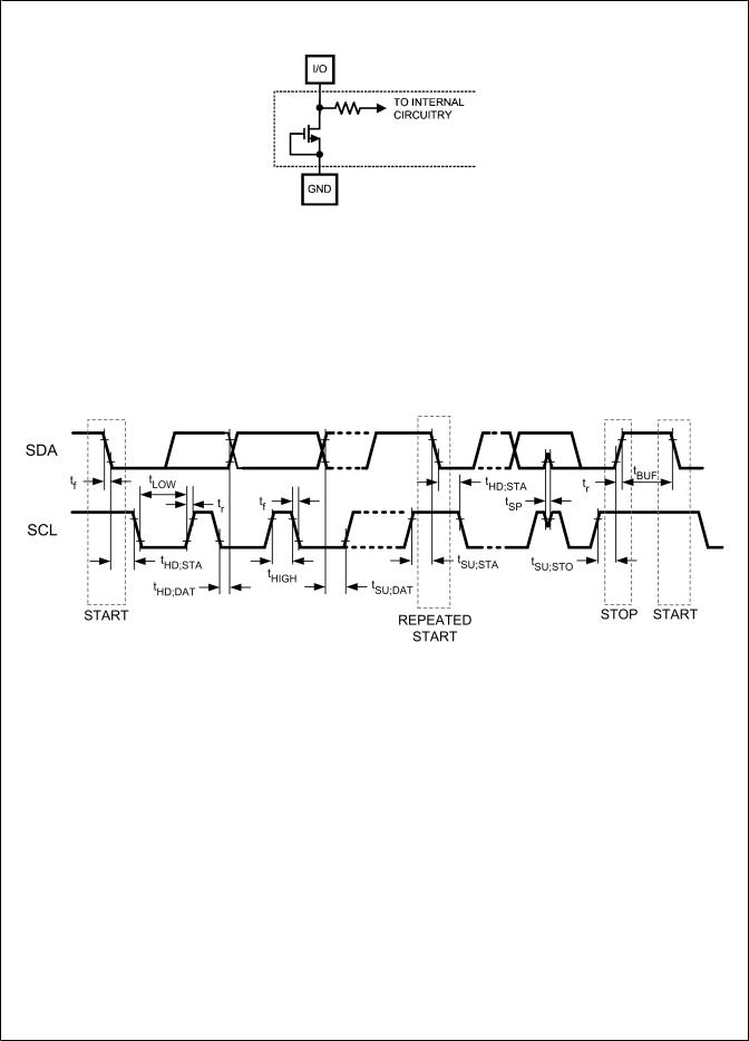
Timing Diagrams
30052060
FIGURE 1. Serial Timing Diagram
ADC101C021/ADC101C027
9 |
www.national.com |
ADC101C021/ADC101C027
Specification Definitions
ACQUISITION TIME is the time required for the ADC to acquire the input voltage. During this time, the hold capacitor is charged by the input voltage.
APERTURE DELAY is the time between the start of a conversion and the time when the input signal is internally acquired or held for conversion.
CONVERSION TIME is the time required, after the input voltage is acquired, for the ADC to convert the input voltage to a digital word.
DIFFERENTIAL NON-LINEARITY (DNL) is the measure of the maximum deviation from the ideal step size of 1 LSB.
EFFECTIVE NUMBER OF BITS (ENOB, or EFFECTIVE BITS) is another method of specifying Signal-to-Noise and Distortion or SINAD. ENOB is defined as (SINAD - 1.76) / 6.02 and says that the converter is equivalent to a perfect ADC of this (ENOB) number of bits.
FULL POWER BANDWIDTH is a measure of the frequency at which the reconstructed output fundamental drops 3 dB below its low frequency value for a full scale input.
GAIN ERROR is the deviation of the last code transition
(111...110) to (111...111) from the ideal (VREF - 1.5 LSB), after adjusting for offset error.
INTEGRAL NON-LINEARITY (INL) is a measure of the deviation of each individual code from a line drawn from negative full scale (½ LSB below the first code transition) through positive full scale (½ LSB above the last code transition). The deviation of any given code from this straight line is measured from the center of that code value.
INTERMODULATION DISTORTION (IMD) is the creation of additional spectral components as a result of two sinusoidal frequencies being applied to an individual ADC input at the same time. It is defined as the ratio of the power in either the second or the third order intermodulation products to the sum of the power in both of the original frequencies. Second order products are fa ± fb, where fa and fb are the two sine wave input frequencies. Third order products are (2fa ± fb ) and (fa ± 2fb). IMD is usually expressed in dB.
MISSING CODES are those output codes that will never appear at the ADC output. The ADC101C021 is guaranteed not to have any missing codes.
OFFSET ERROR is the deviation of the first code transition (000...000) to (000...001) from the ideal (i.e. GND + 0.5 LSB).
SIGNAL TO NOISE RATIO (SNR) is the ratio, expressed in dB, of the rms value of the input signal to the rms value of the sum of all other spectral components below one-half the sampling frequency, not including harmonics or d.c.
SIGNAL TO NOISE PLUS DISTORTION (S/N+D or SINAD) Is the ratio, expressed in dB, of the rms value of the input signal to the rms value of all of the other spectral components below half the clock frequency, including harmonics but excluding d.c.
SPURIOUS FREE DYNAMIC RANGE (SFDR) is the difference, expressed in dB, between the desired signal amplitude to the amplitude of the peak spurious spectral component, where a spurious spectral component is any signal present in the output spectrum that is not present at the input and may or may not be a harmonic.
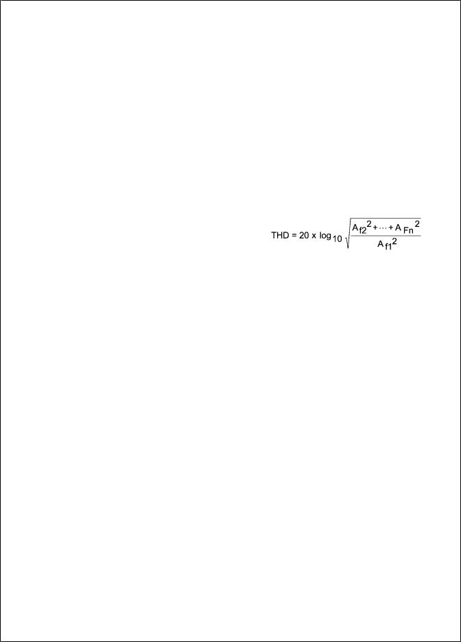
TOTAL HARMONIC DISTORTION (THD) is the ratio, expressed in dBc, of the rms total of the first n harmonic components at the output to the rms level of the input signal frequency as seen at the output. THD is calculated as
where Af1 is the RMS power of the input frequency at the output and Af2 through Afn are the RMS power in the first n harmonic frequencies.
THROUGHPUT TIME is the minimum time required between the start of two successive conversions. It is the acquisition time plus the conversion time.
LEAST SIGNIFICANT BIT (LSB) is the bit that has the smallest value or weight of all bits in a word. This value is
LSB = VA / 2n
where VA is the supply voltage for this product, and "n" is the resolution in bits, which is 10 for the ADC101C021.
MOST SIGNIFICANT BIT (MSB) is the bit that has the largest value or weight of all bits in a word. Its value is 1/2 of VA.
www.national.com |
10 |
 Loading...