


Mitsubishi M16C245M4-XXXGP, M16C245FG-GP, M16C245FC-GP, M16C245FA-GP, M16C245F8-GP Datasheet
...Preliminary Specification
Specifications in this manual are tentative and subject to change
Mitsubishi microcomputers
M30245 Group
Features |
SINGLE-CHIP 16-BIT CMOS MICROCOMPUTER |
1.0 Description
The M30245 group is a 16-bit microcomputer based on the M16C family core technology that uses the high performance silicon gate CMOS process with an M16C/62 Series CPU core, and is packaged in a 100-pin, molded plastic QFP. They are single-chip USB peripheral microcontrollers meeting the Universal Serial Bus (USB) Version 1.1 specification. These microcontrollers operate using sophisticated instructions featuring a high level of instruction efficiency, making them capable of executing instructions at high speed.
1.1 Features
• |
Number of instructions ........................ |
91 |
• Shortest instruction execution time ..... |
83ns f(XIN)=12MHz, Vcc=3V with no wait |
|
• |
USB Features:..................................... |
5 endpoint pairs (IN/OUT) |
|
|
3.25K FIFO |
|
|
Integrated transceiver |
|
|
Conforms to USB V1.1 Specification |
• |
Frequency Synthesizer........................ |
PLL for 48MHz clock |
• Memory capacity................................. |
64KROM/5KRAM |
|
|
|
128K ROM / 10K RAM |
|
|
128K Flash /10K RAM |
• |
Supply Voltage .................................... |
3.0 to 3.6V (f(XIN)=12MHz) |
• |
Interrupts............................................. |
21 internal and 5 external interrupt sources |
|
|
4 software interrupt sources |
|
|
7 levels (including key input interrupt X 8) |
• |
Multifunction 16-bit timer ..................... |
5 output timers+ 3 input timers |
• |
UART................................................... |
3X7/8/9,2X7/8/9/16/24/32bits; |
|
|
Configurable for synchronous or asynchronous mode, I2S, I2C |
• |
DMAC.................................................. |
4 channels |
• |
A-D Converter ..................................... |
10 bits X 8 channels |
• |
CRC calculation circuit ........................ |
2 circuits with MSB/LSB selectable |
• |
Watchdog timer ................................... |
1 line |
• |
Key-on Wake up .................................. |
8 inputs |
• |
Programmable I/O............................... |
84 lines (TBD) |
• |
Clock-generating circuit....................... |
2 built-in clock generation circuit |
|
|
(built-in feedback resistor, and external ceramic or quartz oscillator) |
1.2 Applications
USB peripherals, such as telephones, audio systems, office equipment, communications equipment, portable equipment, scanners, and digital cameras.
1-3
Preliminary Specification
Specifications in this manual are tentative and subject to change
Mitsubishi microcomputers
M30245 Group
Pin Configuration |
SINGLE-CHIP 16-BIT CMOS MICROCOMPUTER |
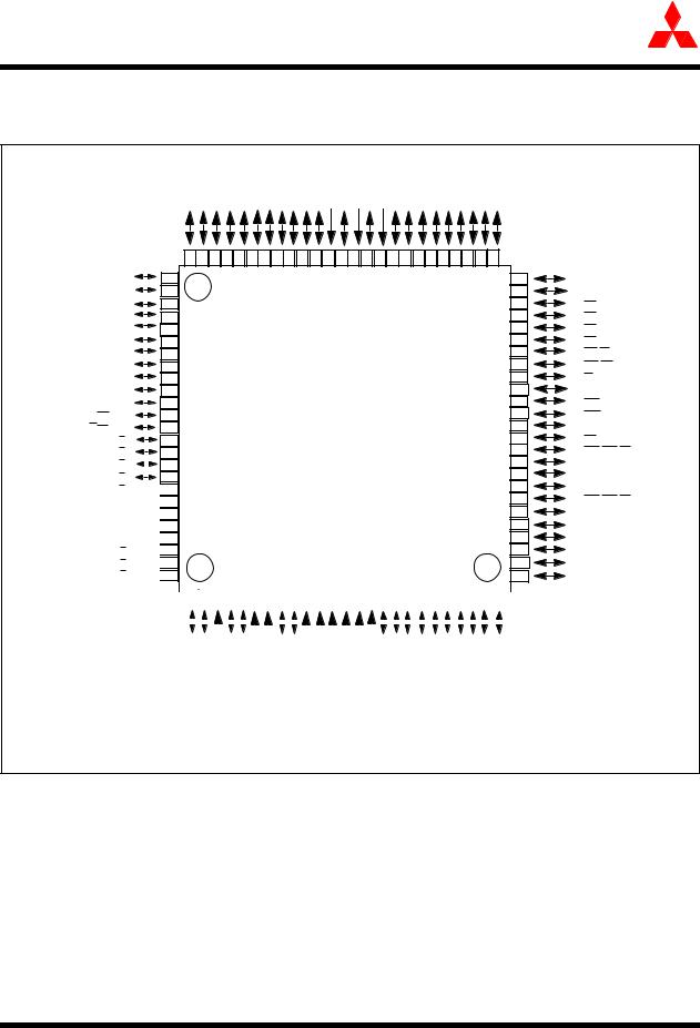
1.3 Pin Configuration
Figure 1.1 shows the pin configuration (top view).
P12/D10/LED2
P11/D9/LED1
P10/D8/LED0
P07/D7
P06/D6
P05/D5
P04/D4
P03/D3
P02/D2
P01/D1
P00/D0
P103/SOF/TB1in
P102/ADTRIG/TB0in
P97/AN7/KI7
P96/AN6/KI6
P95/AN5/KI5
P94/AN4/KI4
P93/AN3/KI3 
 AVss
AVss 
 LPF
LPF 
 Vref
Vref 
 AVcc
AVcc 

P92/AN2/KI2 
 P91/AN1/KI1
 P90/AN0/KI0

76
77
78
79
80
81
82
83
84
85
86
87
88
89
90
91
92
93
94
95
96
97
98
99
100
P13/D11/LED3 |
P14/D12/LED4 |
P15/D13/LED5 |
P16/D14LED6 |
P17/D15LED7 |
P20/A0 |
P21/A1 |
P22/;A2 |
P23/A3 |
P24/A4 |
P25/A5 |
P26/A6 |
P27/A7 |
Vss |
P30/A8 |
Vcc |
P31/A9 |
P32/A10 |
P33/A11 |
P34/A12 |
P35/A13 |
P36/A14 |
P37/A15 |
P40/A16 |
P41/A17 |
75 |
74 |
73 |
72 |
71 |
70 |
69 |
68 |
67 |
66 |
65 |
64 |
63 |
62 |
61 |
60 |
59 |
58 |
57 |
56 |
55 |
54 |
53 |
52 |
51 |
M30245Mx/FC
100-pin QFP (0.5mm pitch)
|
1 |
2 |
3 |
4 |
5 |
6 |
7 |
8 |
9 |
10 |
11 |
12 |
13 |
14 |
15 |
16 |
17 |
18 |
19 |
20 |
21 |
22 |
23 |
24 |
25 |
|
|
|
|
|
|
|
|
|
|
|
|
|
|
|
|
|
|
|
|
|
|
|
|
|
|
|
|
|
|
|
|
|
|
|
|
|
|
|
|
|
|
|
|
|
|
|
|
|
|
|
|
|
|
|
|
|
|
|
|
|
|
|
|
|
|
|
|
|
|
|
|
|
|
|
|
|
|
|
|
|
|
|
|
|
|
|
|
|
|
|
|
|
|
|
|
|
|
|
|
|
|
|
|
|
|
|
|
|
|
|
|
|
|
|
|
|
|
|
|
|
|
|
|
|
|
|
|
|
|
|
|
|
|
|
|
|
|
|
|
|
|
|
|
|
|
P101/VbusDTCT |
|
P100/CTS4/RTS4/SS4/TB2in/ATTACH |
Ext Cap |
USBD+ |
USB D- |
BYTE |
|
CNVss |
P87/XCin |
P86/XCout |
RESET |
Xout |
Vss |
Xin |
Vcc |
P85/NMI |
|
P84/INT2 |
|
P83/INT1 |
|
P82/CLK4/INT0 |
P81/RxD4/SCL4/STxD4//TA4in |
P80/TxD4/SDA4/SRxD4//TA4out |
|
P77/CTS3/RTS3/SS3//TA3in |
P76/CLK3/TA3out |
P75/RxD3/SCL3/STxD3/TA2in |
P74/TxD3/SDA3/SRxD3/TA2out |
|
P73/CTS2/RTS2/SS2/TA1in |
|||||||||||||||||||||||||||
|
|
|
|
|
||||||||||||||||||||||||||||||||||||||||||||||||||||||
|
|
|
|
|
|
|
|
|
|
|||||||||||||||||||||||||||||||||||||||||||||||||
|
|
|
|
|
|
|
|
|
|
|
|
|
|
|||||||||||||||||||||||||||||||||||||||||||||
|
|
|
|
|
|
|
|
|
|
|
|
|
|
|
|
|
|
|
|
|
|
|
||||||||||||||||||||||||||||||||||||
|
|
|
|
|
|
|
|
|
|
|
|
|
|
|
|
|
|
|
|
|
|
|
|
|
|
|
|
|
|
|
|
|
|
|
|
|
||||||||||||||||||||||
|
|
|
|
|
|
|
|
|
|
|
|
|
|
|
|
|
|
|
|
|
|
|
|
|
|
|
|
|
|
|
|
|
|
|
|
|||||||||||||||||||||||
|
|
|
|
|
|
|
|
|
|
|
|
|
|
|
|
|
|
|
|
|
|
|
|
|
|
|
|
|
|
|
|
|
|
|
|
|
|
|||||||||||||||||||||
|
|
|
|
|
|
|
|
|
|
|
|
|
|
|
|
|
|
|
|
|
|
|
|
|
|
|
|
|
|
|
|
|
|
|
|
|
|
|
|
|
||||||||||||||||||
|
|
|
|
|
|
|
|
|
|
|
|
|
|
|
|
|
|
|
|
|
|
|
|
|
|
|
|
|
|
|
|
|
|
|
|
|
|
|
|
|
|
|
|
|||||||||||||||
|
|
|
|
|
|
|
|
|
|
|
|
|
|
|
|
|
|
|
|
|
|
|
|
|
|
|
|
|
|
|
|
|
|
|
|
|
|
|
|
|
|
|
||||||||||||||||
|
|
|
|
|
|
|
|
|
|
|
|
|
|
|
|
|
|
|
|
|
|
|
|
|
|
|
|
|
|
|
|
|
|
|
|
|
|
|
|
|
|
|
|
|||||||||||||||
|
|
|
|
|
|
|
|
|
|
|
|
|
|
|
|
|
|
|
|
|
|
|
|
|
|
|
|
|
|
|
|
|
|
|
|
|
|
|
|
|
|
|
|
|||||||||||||||
|
|
|
|
|
|
|
|
|
|
|
|
|
|
|
|
|
|
|
|
|
|
|
|
|
|
|
|
|
|
|
|
|
|
|
|
|
|
|
|
|
|
|
|
|
|
|
|
|
|
|||||||||
50 |
P42/A18 |
49 |
P43/A19 |
48 |
P44/CS0 |
47 |
P45/CS1 |
46 |
P46/CS2 |
45 |
P47/CS3 |
44 |
P50/WRL/WR |
43 |
P51/WRH/BHE |
42 |
P52/RD |
41 |
P53/BCLK |
40 |
P54/HLDA |
39 |
P55/HOLD |
38 |
P56/ALE |
37 |
P57/RDY/CLKOUT |
36 |
P60/CTS0/RTS0/SS0 |
35 |
P61/CLK0/SCK0 |
34 |
P62/RxD0/SCL0/STxD0/WS0 |
33 |
P63/TxD0/SDA0/SRxD0/SD0 |
32 |
P64/CTS1/RTS1/SS1 |
31 |
P65/CLK1/SCK1 |
30 |
P66/RxD1/SCL1/STxD1/WS1 |
29 |
P67/TxD1SDA1/SRxD1/SD1 |
28 |
P70/TxD2/SDA2/SRxD2/TA0out |
27 |
P71/RxD2/SCL2/STxD2/TA0in |
26 |
P72/CLK2/TA1out |
Figure 1.1: Pin Configuration (top view)
1-4

Preliminary Specification
Specifications in this manual are tentative and subject to change
Mitsubishi microcomputers
M30245 Group
Block Diagram |
SINGLE-CHIP 16-BIT CMOS MICROCOMPUTER |
1.4 Block Diagram
Figure 1.2 is a block diagram of the M30245 group.
8 |
8 |
8 |
8 |
8 |
8 |
8 |
Port P0 |
Port P1 |
Port P2 |
Port P3 |
Port P4 |
Port P5 |
Port P6 |
Internal Peripheral Functions
Timers
Timer TA0 (16 bits)
Timer TA1 (16 bits)
Timer TA2 (16 bits)
Timer TA3 (16 bits)
Timer TA4 (16 bits)
Timer TB0 (16 bits)
Timer TB1 (16 bits)
Timer TB2 (16 bits)
System Clock Generator
Xin - Xout
Xcin - Xcout
CRC Arithmetic Circuit
(X16+X12+X5+1, X16+X15+X2+1)
DMAC
(4 channels)
Memory
USB FIFO (3.25K bytes)
ROM/FLASH (128K bytes)
RAM (10K bytes)
UART/Clock Synchronous SI/O |
M16C/62 16-bit CPU Core |
||
|
|
|
|
(8 bits X 5 channels) |
Registers |
Program counter |
|
|
R0H |
R0L |
PC |
|
R0H |
R0L |
|
A-D Converter |
R1H |
R1L |
Vector table |
R1H |
R1L |
||
(10 bits X 8 channels) |
R2 |
|
INTB |
R2 |
|||
|
R3 |
|
|
|
R3 |
|
|
|
A0 |
|
Stack pointer |
Watchdog Timer |
A0 |
||
A1 |
|
ISP |
|
(15 bits) |
A1 |
||
FB |
|
USP |
|
|
FB |
||
USB Function |
SB |
|
|
|
|
|
|
with frequency synthesizer |
FLG |
Multiplier |
|
|
|
||
8 |
|
Port P7 |
|
P8 Port |
7 |
P8 Port |
1 |
5 |
|
P9 Port |
8 |
P10 Port |
|
0 |
4 |
10- |
|
3 |
|
Figure 1.2: Block diagram of M30245 group
1-5

Preliminary Specification
Specifications in this manual are tentative and subject to change
Mitsubishi microcomputers
M30245 Group
Performance outline |
SINGLE-CHIP 16-BIT CMOS MICROCOMPUTER |
1.5 Performance outline
Table 1.1 is a performance outline of the M30245 group.
Table 1.1: |
Performance outline of M16C/M30245 Group |
||||
|
|
|
|
|
|
|
Parameters |
|
Function Description |
||
|
|
|
|||
|
|
|
|||
Number of basic Instructions |
|
91 |
|||
|
|
|
|||
Shortest Instruction execution time |
|
83 ns f(Xin)= 12 MHz, Vcc = 3V |
|||
|
|
|
|
|
|
Memory size |
|
ROM |
|
128/64 Kbytes |
|
|
|
|
|
|
|
|
RAM |
|
10/5 Kbytes |
||
|
|
|
|||
|
|
|
|
|
|
Input/Output ports |
P0~P9 |
|
I/O |
8 bits x 10 |
|
|
|
|
|
||
P100~P101 |
|
I/O |
2 bits x 1 |
||
|
|
|
|||
|
|
|
|
|
|
Multifunction timer |
TA0, TA1, TA2, TA3, TA4 |
16 bits x 5 |
|||
|
|
|
|
||
TB0, TB1, TB2 |
|
16 bits x 3 |
|||
|
|
|
|||
|
|
|
|
|
|
Serial I/O |
|
UART0~1 |
|
UART (or clock synchronous or IIS) x 2 |
|
|
|
|
|
|
|
|
UART2~4 |
|
UART (or clock synchronous) x 3 |
||
|
|
|
|||
|
|
|
|
|
|
A-D converter |
|
|
|
|
10 bits x 8 channels |
|
|
|
|
|
|
DMAC |
|
|
|
|
4 channels |
|
|
|
|||
CRC calculation circuits |
|
CRC-CCITT and CRC-16 |
|||
|
|
|
|||
Watchdog timer |
|
15 bits x 1 (prescaler) |
|||
|
|
|
|
|
|
Interrupts |
|
|
|
|
21 internal, 4 external sources, 4 software, 7 levels |
|
|
|
|||
Clock-generating circuit |
|
2 built-in clock generating circuit |
|||
|
|
|
|||
Supply voltage |
|
3.0 ~ 3.6V, f(XIN) = 12MHz |
|||
|
|
|
|||
Power consumption |
|
TBD |
|||
|
|
|
|
|
|
I/O characteristics |
I/O withstand voltage |
|
3V |
||
|
|
|
|
||
Output current |
|
5mA (20mA available on P1, P70, P72, P74, P76, P80) |
|||
|
|
|
|||
|
|
|
|
|
|
Operating temperature |
|
-20 to 85 C |
|||
|
|
|
|||
Device configuration |
|
CMOS high performance silicon gate |
|||
|
|
|
|
|
|
Package |
|
|
|
|
100-pin plastic mold QFP |
|
|
|
|
|
|
1-6
 Loading...