

MITSMI MM1313AD, MM1313BD Datasheet

MITSUMI
I
2
C BUS Control 5-Input 2-Output AV Switch MM1313
I2C BUS Control 5-Input 2-Output AV Switch
Monolithic IC MM1313
Outline
This IC is a 5-input 2-output AV switch with I2C control, developed for use in televisions. Two outputs enable
it to support two screens or "picture-in-picture".
Features
1. Serial control by I2C bus.
2. 5-inputs, 2-outputs.
3. Video and audio system switches can be controlled independently.
4. 6dB amplifier built in to video system.
5. Built-in Y/C MIX circuit.
6. Slave address can be changed : 90H or 92H.
7. Audio muting possible by external pin.
8. Maintains high impedance even when I
2
C BUS line (SDA, SCL) power supply is off.
9. Built-in 3 value discrimination function.
10.On-chip power ON reset function.
11.Two types of audio input impedance : 60kΩ and 30kΩ.
MM1313AD : 60kΩ MM1313BD : 30kΩ
12.Supports 2-screen or P-IN-P TV.
Package
SDIP-42A (MM1313AD, MM1313BD)
Applications
1. Televisions
2. Other video equipment
MITSUMI
I
2
C BUS Control 5-Input 2-Output AV Switch MM1313
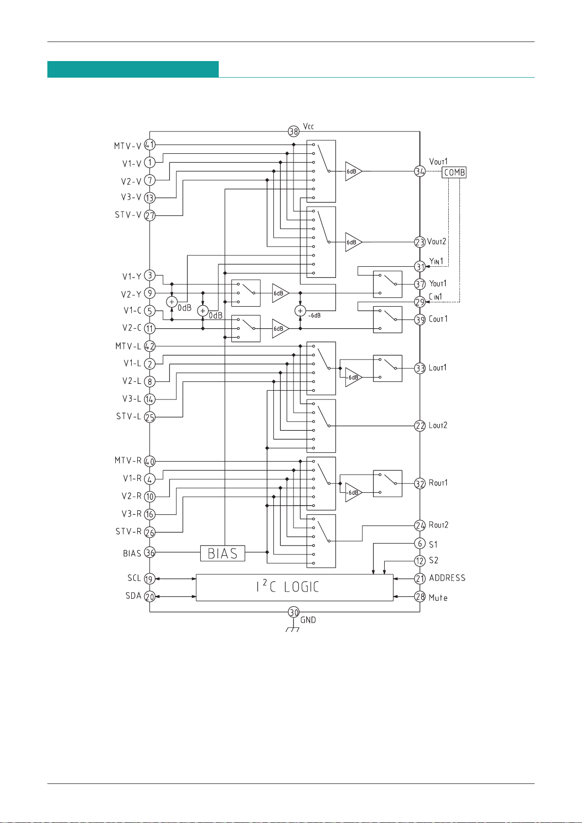
Equivalent Block Diagram
MITSUMI
I
2
C BUS Control 5-Input 2-Output AV Switch MM1313
Pin Function
Pin No.
Name
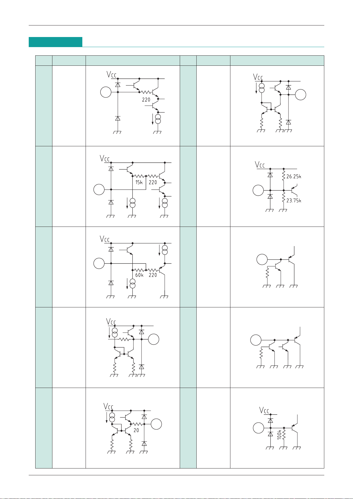
Internal equivalent circuit diagram
Pin No.
Name
Internal equivalent circuit diagram
41 MTV-V
1 V1
-
V
7 V2
-
V
13 V3
-
V
27 STV
-
V
3 V1
-
Y
9 V2
-
Y
31 Y
IN1
5 V1-C
11 V2
-
C
29 C
IN1
42 MTV-L
2 V1
-
L
8 V2
-
L
14 V3
-
L
25 STV
-
L
40 MTV
-
R
4 V1
-
R
10 V2
-
R
16 V3
-
R
26 STV
-
R
34 VOUT1
23 V
OUT2
37 YOUT1
39 C
OUT1
33 LOUT1
22 L
OUT2
32 R
OUT1
24 R
OUT2
36 BIAS
19 SCL
20 SDA
6 S1
12 S2
21 ADR
28 Mute
MITSUMI
I
2
C BUS Control 5-Input 2-Output AV Switch MM1313
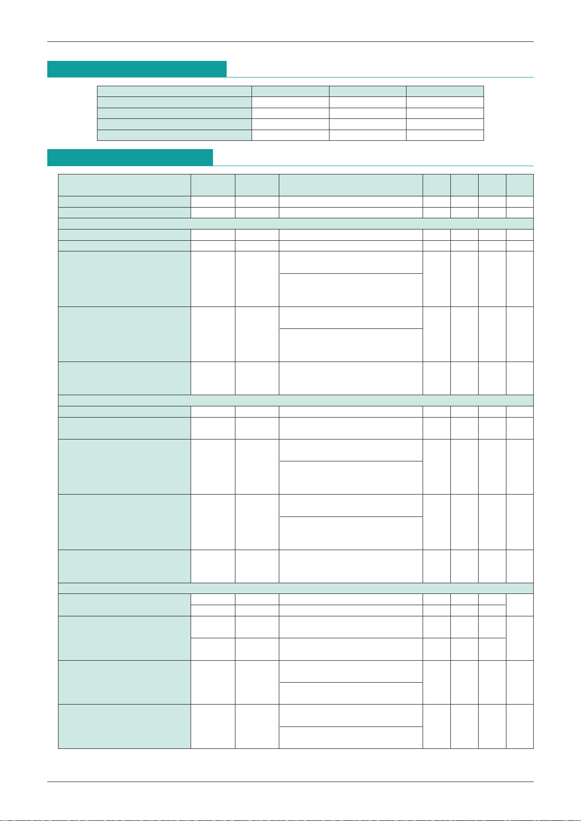
Absolute Maximum Ratings
(Ta=25°C)
Item Symbol Ratings Units
Storage temperature T
STG
-
40~+125
°
C
Operating temperature T
OPR
-
20~+75
°
C
Power supply voltage V
CC 12 V
Allowable power dissipation Pd 850 mW
Electrical Characteristics
(Ta=25°C, VCC=9V)
Item Symbol
Measure
Conditions (unless otherwise indicated,
Min. Typ. Max. Units
ment pin
Measurement Circuit Figure 1)
Operating power supply voltage
VCC 8 9 10 V
Current consumption I
CC 38 VCC=9V, no signal, no load 40 52 mA
V
OUT1 output
Voltage gain G
V1 TP1 Sine wave 1.0VP-P, 100kHz 5.5 6.0 6.5 dB
Frequency characteristics F
V1 TP1
Sine wave 1.0V
P-P
, 10MHz/100kHz-1.0 0 1.0 dB
Vn-V : Staircase 1V
P-P
APL=10~90%
Differential gain DG
V1 TP1
Vn-Y : Staircase (luminance signal) 1V
P-P
-
30 3 %
Vn-C : Chroma signal 0.3V
P-P
APL=10~90%
Vn-V : Staircase 1V
P-P
APL=10~90%
Differential phase DP
V1 TP1
Vn-Y : Staircase (luminance signal) 1V
P-P
-
3 0 3 deg
Vn-C : Chroma signal 0.3V
P-P
APL=10~90%
Sine wave 100kHz
Input dynamic range D
V1 SG1~3 Maximum input for total higher 1.6 1.9 VP-P
harmonic distortion factor < 1.0%
V
OUT2 output
Voltage gain G
V2 TP6 Sine wave 1.0VP-P, 100kHz 5.5 6.0 6.5 dB
Frequency characteristics F
V2 TP6
Sine wave 1.0V
P-P
-
1.0 0 1.0 dB
10MHz/100kHz
Vn-V : Staircase 1V
P-P
APL=10~90%
Differential gain DG
V2 TP6
Vn-Y : Staircase (luminance signal) 1V
P-P
-
30 3 %
Vn-C : Chroma signal 0.3V
P-P
APL=10~90%
Vn-V : Staircase 1V
P-P
APL=10~90%
Differential phase DP
V2 TP6
Vn-Y : Staircase (luminance signal) 1V
P-P
-
3 0 3 deg
Vn-C : Chroma signal 0.3V
P-P
APL=10~90%
Sine wave 100kHz
Input dynamic range D
V2 SG1~3 Maximum input for total higher 1.6 1.9 VP-P
harmonic distortion factor < 1.0%
YOUT1 output
Voltage gain
G
Y1 TP2
Vn-Y : Sine wave 1.0V
P-P
, 100kHz
5.5 6.0 6.5
dB
G
Y2 TP2
YIN1 : Sine wave 2.0V
P-P
, 100kHz-0.5 0 0.5
F
Y1 TP2
Vn
-
Y : Sine wave 1.0VP
-
P
-
1.0 0 1.0
Frequency characteristics
10MHz/100kHz
dB
F
Y2 TP2
Y
IN1 : Staircase 2.0VP-P
-
1.0 0 1.0
10MHz/100kHz
Vn-Y : Staircase 1V
P-P
Differential gain DGY TP2
APL=10~90%
-
30 3 %
Y
IN1: Staircase 2VP-P
APL=10~90%
Vn-Y : Staircase 1V
P-P
Differential phase DPY TP2
APL=10~90%
-
3 0 3 deg
Y
IN1 : Staircase 2VP-P
APL=10~90%
 Loading...