

MITSMI MM1089XF Datasheet

MITSUMI
Sensor Amplifier MM1089
Sensor Amplifier
Monolithic IC MM1089
Outline
This IC is an amplifier with a high-impedance differential input, which can be used in high-CMR instrumentation.
Particularly when amplifying signals from a high-impedance or high-bias signal source, often signals are buried
in noise, making amplification difficult. This IC amplifies only the signal, and the noise is suppressed rather than
amplified, making it effective for use where noise is prominent or with high-impedance signal sources.
Features
1. Battery charge/discharge current detection
(for laptops, word processors, etc) 80dB min., 100dB typ.
2.
Signal amplifiers for magnetic sensors, pressure sensors, strain gauges
Except 10MΩ
3. Instrumentation amps 3~ 100
4. Broad input range
-
0.3V~VCC+0.3V
5. Two internal channels
Package
SOP-18A (MM1089XF)
Applications
1 Detection of battery charge/discharge current (for notebook computers, word processors etc)
2 Amplification of magnetic sensor, pressure sensor, strain gauge, other signals
3 Instrumentation amp
MITSUMI
Sensor Amplifier MM1089
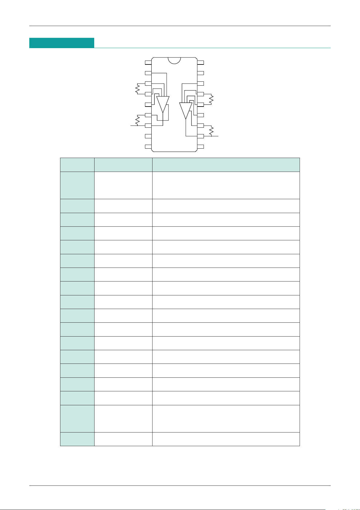
Pin Assignment
1
+IN1
Rg1
-
IN1
OUT1
Rs1
O.COM1
GND
2
3
4
5
6
7
8
9
18
VCC
+IN2
Rg2
+
-
-
IN2
Rs2
OUT2
O.COM2
+
-
O.COM2
17
16
15
14
13
12
11
10
A1
A2
Input range
switching 1
Input range
switching 2
Pin no. Pin name Function
1
Input range switching 1
AMP1 Input voltage range switching
INCHG1 Hi : 1.8V~V
CC+0.3V LO :
-
0.3V~VCC-1.8V
2 IN1+ AMP1 +Input
3 Rg1+ AMP1 Resistance to set the Rg gain
4 Rg1
-
AMP1 Resistance to set the Rg gain
5 IN1
-
AMP1 -Input
6 Rs1 AMP1 Resistance to set the Rs gain
7 OUT1 AMP1 Resistance to set the Rs gain, output 1
8 O.COM1 AMP1 Common output
9 GND Ground
10 O.COM2 AMP2 Common output
11 OUT2 AMP2 Resistance to set the Rs gain, output 2
12 Rs2 AMP2 Resistance to set the Rs gain
13 IN2
-
AMP2 -Input
14 Rg2
-
AMP2 Resistance to set the Rg gain
15 Rg2+ AMP2 Resistance to set the Rg gain
16 IN2+ AMP2 +Input
17
Input range switching 2
AMP2 Input voltage range switching
INCHG2 Hi : 1.8V~V
CC+0.3V Lo :
-
0.3V~VCC-1.8V
18 V
CC Power supply input
MITSUMI
Sensor Amplifier MM1089
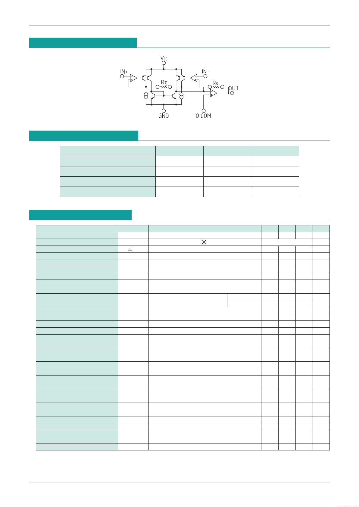
Equivalent Circuit Diagram
Absolute Maximun Ratings
(Ta=25°C)
Item Symbol Ratings Units
Operating temperature T
OPR
-
20~+70 °C
Storage temperature T
STG
-
40~+125 °C
Power supply voltage V
CC
-
0.3~+25 V
Allowable loss Pd 350 mW
Electrical Characteristics
(Except where noted otherwise, Ta=25°C, V
CC
=15V, Rg=10kΩ, Rs=1000kΩ)
Item Symbol Measurement conditions Min. Typ. Max. Units
Consumption current I
CC 0.45 0.6 mA
Gain G
V GV=K Rs/Rg See Fig. 1
Gain error G
V Error of above formula
-
5 0 +5 %
Input bias current 1 I
B1 When input range switching pin is high 50 250 nA
Input bias current 2 I
B2 When input range switching pin is low
-
100-500 nA
Input offset current I
IO 550nA
Input offset voltage V
IO
-
2 0 +2 mV
O.COM pin setting
V
OC
Output takes O.COM pin
1.0
VCC-
1.5
V
voltage range voltage as reference
O.COM pin
I
OC
MM1089
-
50
nA
input bias current MM1131
-
100
Output offset voltage V
OO VOC as reference (GV=40dB)
-
0.25
0
+0.25
V
Output offset current I
OO VOC as reference (GV=40dB)
-
0.25
0
+0.25
µA
Common-mode input range 1
VICM1 When input range switching pin is high 1.8
VCC+0.3
V
Common-mode input range 2
VICM2 When input range switching pin is low
-
0.3
VCC-
1.8
V
Input voltage high level
V
HSW
2.4 V
for input range switching pin
Input voltage low level
VLSW 0.8 V
for input range switching pin
Input current (Hi) for
I
HSW VINSW=15V
-
11µA
input range switching pin
Input current (Lo) for
I
LSW VINSW=0V
-
5
-
0.5 µA
input range switching pin
Output outflow current I
SOURC
VIN(+)-VIN(
-
)=+1V, VO=VCC
-
1.5V
1.0 4.0 mA
O.COM=5V
Output inflow current I
SINK
VIN(+)-VIN(
-
)=
-
1V, VO=0.3V
0.3 1.0 mA
O.COM=5V
Slew rate SR 0.16 V/µS
Common-mode signal rejection ratio
CMR DC 80 100 dB
Power supply fluctuation
SVR DC 80 100 dB
rejection ratio
Input equivalent noise voltage
VNI RIN=1kΩ, BPF=20Hz~20kHz 6 µV
 Loading...