

MITSMI MM1081XV, MM1027NV, MM1027XD, MM1027XF, MM1027XV Datasheet
...
MITSUMI
System Reset (with battery back-up) MM1027, 1081
System Reset (with battery back-up)
Monolithic IC MM1027, 1081
Outline
These ICs were developed for STATIC-RAM (S-RAM) battery back-up, and have built-in switching circuit for
main power supply and battery, back-up timing circuit and battery checker.
Power ON/OFF and momentary power interruptions can damage S-RAM data on equipment that contains an
S-RAM. These ICs switch the S-RAM to back-up mode (CS signal makes S-RAM CE pin low and CE
when power supply voltage goes below a set voltage (detection voltage 4.2V typ., variable), preventing
damage to data. Further, when power supply voltage drops, these ICs switch from main power supply to
battery back-up (switching voltage 3.3V typ.). Then, when power supply voltage rises, they first switch the SRAM from battery back-up state to main power supply (switching voltage 3.3V typ.), and from back-up mode
to normal mode (CS signal makes S-RAM CE pin high and CE
--------------------------------------------------
pin low). These signal processes provide
reliable protection against data damage. The CS signal also can absorb power supply chattering and
roughness through the external capacitor.
There is a built-in battery checker to monitor the back-up battery voltage, and this circuit is turned ON/OFF by
the control pin.
---------------------------------------------------
pin high)
Features
1. Battery back-up
1. Low IC current consumption (loss current) 0.3µA typ.
2. Drop voltage inside IC (input/output voltage difference) I
3. Reverse current (reverse leak current) 0.1µA max.
2. Normal operation
MM1027
Drop voltage inside IC (input/output voltage difference) I
Output voltage V
CC=5V IO=10mA 4.8V typ.
Current consumption D.CONT OPEN 3.0mA max.
External transistor drive current 25mA typ.
MM1081
Drop voltage inside IC (input/output voltage difference) I
Output voltage V
CC=5V IO=120mA 4.75V typ.
Current consumption 350µA max.
External transistor drive current (for output current increase) 25mA typ.
TC source current 3.0µA typ.
3. Battery-Vcc switching voltage 3.3V typ.
4. Detection voltage (CS, CS
------------------------------------------------
) variable 4.2V typ.
5. Battery checker 1 X type 2.70V typ.
N type 2.50V typ.
6. Battery checker 2 X type 2.55V typ.
N type 2.35V typ.
O=10µA 0.2V typ.
O=70mA 0.2V typ.
O=120mA 0.25V typ.
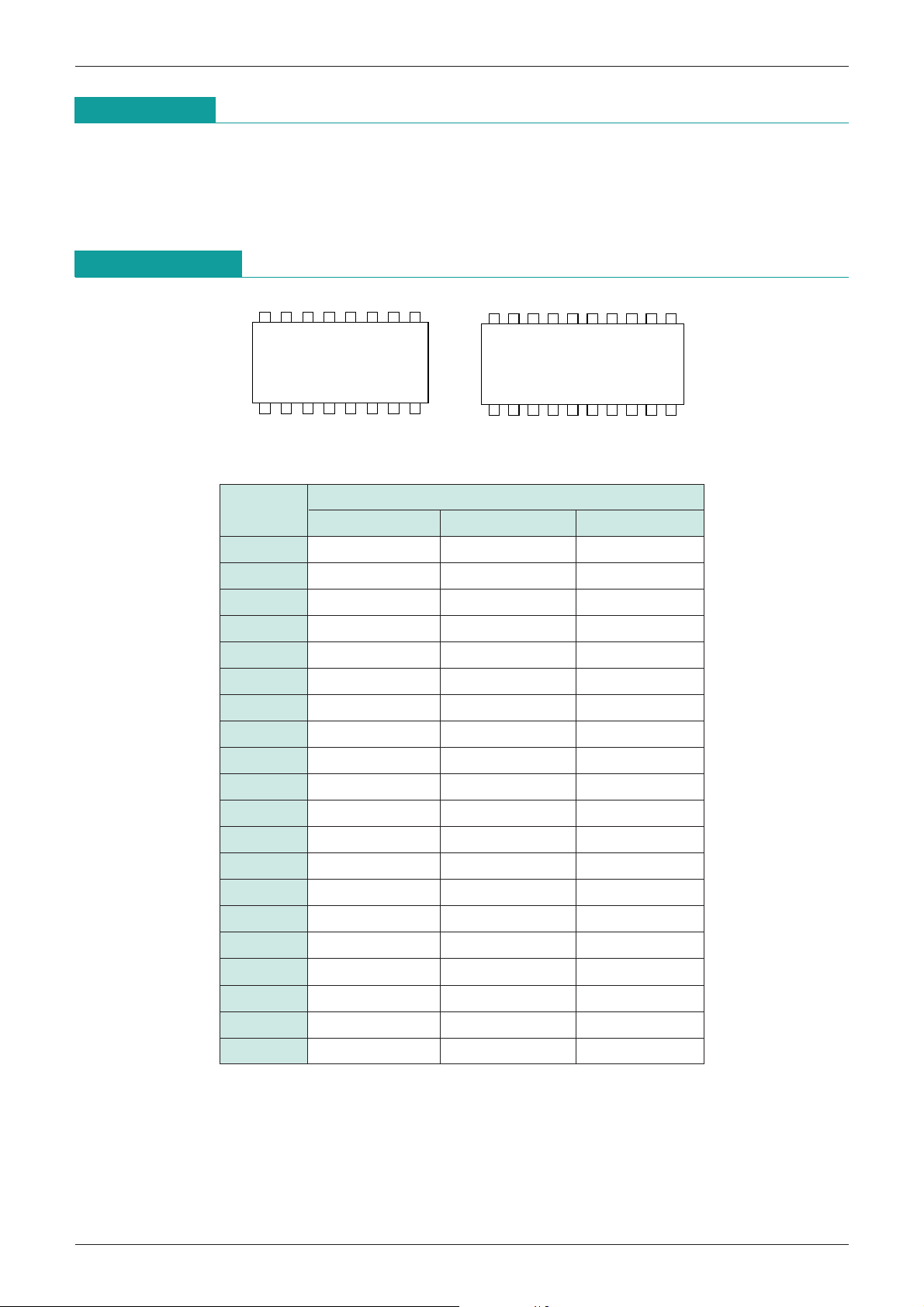
Package
TSOP-20A (MM1027XV, MM1027NV, MM1081XV)
SOP-16A (MM1027XF, MM1027NF)
DIP-16A (MM1027XD)
MITSUMI
SOP-16A/DIP-16A
13 762458
16 13 1115 14 12910
TSOP-20A
13 6824579
10
20 16 1319 17 15 14 1218 11
System Reset (with battery back-up) MM1027, 1081
Applications
1. IC memory cards (RAM cards)
2. PCs, word processors
3. Fax machines, photocopiers, other office equipment
4. Other equipment with S-RAMs (equipment requiring back-up)
Pin Assignment
Pin no.
Function
TSOP-20A SOP-16A DIP-16A
1 GND GND GND
2 ADJ. NC NC
3 NC ADJ. ADJ.
4 TC TC T
C
5 NC CS CS
6 CS NC NC
7 NC CS
---------------------------------------------------
8 CS
---------------------------------------------------
DET.CONT DET.CONT
---------------------------------------------------
CS
9 NC Bat.DET1 Bat.DET1
10 DET.CONT NC NC
11 Bat.DET1 Bat.DET2 Bat.DET2
12 NC Battery Battery
13 Bat.DET2 V
OUT VOUT
14 NC External drive External drive
15 Battery NC NC
16 NC V
CC VCC
17 VOUT
18 NC
19 External drive
20 V
CC
MITSUMI
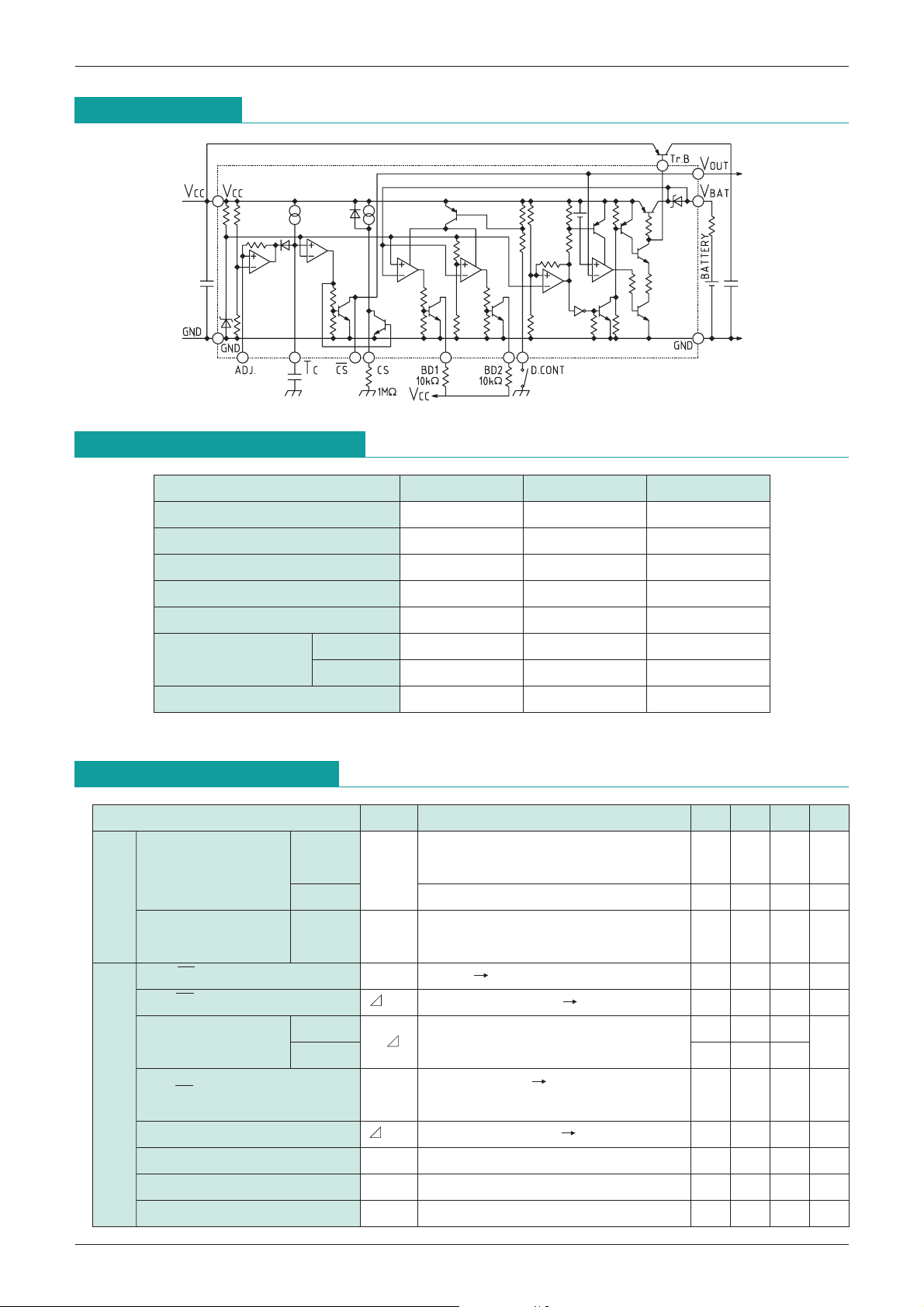
Block Diagram
System Reset (with battery back-up) MM1027, 1081
Absolute Maximum Ratings
Item Symbol Rating Units
Storage temperature T
Operating temperature T
Power supply voltage V
Operating voltage V
Allowable loss Pd 300 mW
Output current
Output current I
Note : IO1 expresses VCC output current value, and IO2 expresses VBATT output current value.
Electrical Characteristics
Item Symbol Measurement conditions Min. Typ. Max. Units
Consumption MM1027
current 1
All
circuits
Consumption
current 2
MM1027 I
MM1081 I
(Except where noted otherwise, Ta=25°C, VCC=5V, V
MM1081 V
MM1027 I
(Ta=25°C)
STG
OPR
CC max. 7 V
CCOP 7V
O190mA
O1 120 mA
O2 200 µA
V
CC=5V, VBAT=3V, IO=0mA
I
CC1 D.CONT pin : OPEN
CC=5V, VBAT=3V, IO=0mA 150 210 350 µA
V
CC2
CC=5V, VBAT=3V, IO=0mA
-
40~+125
-
20~+70
D.CONT pin : GND
°
C
°
C
BAT
=3V)
0.9 1.7 3.0 mA
1.2 2.2 3.5 mA
---------------------------------
CS•CS
circuit
unit
CS, CS detection voltage 1 V
CS, CS hysteresis voltage 1
Detection voltage
temperature characteristic
MM1027
MM1081
S/ T
V
CS, CS detection voltage 2
CS, CS hysteresis voltage 2
CS output voltage L V
CS output voltage H V
CS source current I
S1VCC=H L, VBAT=3V, ADJ pin : OPEN 4.05 4.20 4.35 V
VS1VCC=L H 0.05 0.10 0.20 V
±0.08
%/°C
±0.06
VS2
CC=H L, VBAT=3V
ADJ pin : 12kΩ PULL UP (to V
CC)
3.25 3.50 3.75 V
V
VS2VCC=L H 0.05 0.10 0.20 V
CSL VCC=3V, ICS=3µA 0.05 0.10 V
CSH VCC=5V, ICS=
CSH VCC=5V, VCS=4.6V current measured 8 15 µA
-
3µA 4.85 4.95 V
MITSUMI
System Reset (with battery back-up) MM1027, 1081
Electrical Characteristics
Item Symbol Measurement conditions Min. Typ. Max. Units
CS sync current I
-----------------------------------------------------
CS
output voltage L VCC=5V, ICS=3µA
-----------------------------------------------------
CS
output voltage H VCC=4V, VOUT-VCSH, ICS=-3µA
-----------------------------------------------------
CS
-----------------------------------------------------
•
CS
CS
circuit
unit
BD
circuit
unit
sync current VCC=5V, VCS=0.4V Current measured 0.3 1.0
Operation limit voltage L V
ON delay time 1 t
OFF delay time 1 t
ON delay time 2 t
OFF delay time 2 t
BATT
detection voltage 1
MM1027X
MM1081N
BATT hysteresis voltage 1
BATT
detection voltage 2
MM1027X
MM1081N
BATT hysteresis voltage 2
BD output voltage L VBDL V
(Except where noted otherwise, Ta=25°C, VCC=5V, V
CSL VCC=3.5, VCS=0.4V Current measured 0.5 2.0
--------------------------------------------------------------------
VCSL
--------------------------------------------------
VCSH
---------------------------------------------------------------
ICSL
Minimum power supply voltage at which
OPL
CS pin can hold low level V
PLH1VCC=L H, TC : OPEN, C1=47pF
PHL1VCC=H L, TC : OPEN, C1=47pF
PLH2VCC=L H, TC : 1nF, C1=47pF
PHL2VCC=H L, TC : 1nF, C1=47pF
V
CC=5V, R1=10kΩ PULL UP
<
CS
0.4V
=
VBD1
VBAT=H L (to VCC)
V
CC=5V, R1=10kΩ PULL UP
VBD1
BAT=L H(to VCC)
V
V
CC=5V, R2=10kΩ PULL UP
VBD2
VBAT=H L (to VCC)
V
CC=5V, R2=10kΩ PULL UP
VBD2
BAT=L H (to VCC)
V
CC=5V, VBAT=0V
BAT
=3V)
-
mA
-
0.10 0.25 V
-
0.14 0.40 V
-
mA
-
2.0 2.4 V
-
30
-
µS
-
2.0 5 µS
-
0.8
-
mS
-
2.0 10 µS
2.60 2.70 2.80 V
0.05 0.10 0.20 V
2.45 2.55 2.65 V
0.05 0.10 0.20 V
-
0.2 0.4 V
Backup
circuit
unit
BD output sink current
Leakage current IBDH V
IBDSNK
VCC=5V, VBAT=0V, VBD=4V 1.0 3.0
CC=5V, VBAT=3V, VBD=5V
I/O voltage MM1027
V
SAT1
difference 1 MM1081 V
I/O voltage difference 2 V
I/O voltage difference 3 V
External transistor driving current
Power supply switching voltage
Hysteresis voltage V
Switching voltage
temperature characteristic
MM1027
MM1081 ±0.06
SAT2VBAT=3V, IO=10µA
SAT3VBAT=3V, IO=100µA
IBUD VCC=5V, V (TB) =4.5V 16 25
VBB VCC=H L, VBAT=3V 3.15 3.30 3.45 V
BB VCC=L H, VBAT=3V 0.05 0.10 0.20 V
BB/ T
V
VCC=0V, VBAT=3V, IO=0µA
Loss current I
LOS
D.CONT pin : GND
VCC=0V, VBAT=3V, IO=0µA
Reverse current I
OREV
D.CONT pin : OPEN
TC source current I
TCSCE VCC=5V, VTC=0V 2.0 3.0 5.0 µA
CC=5V, IO=70mA
V
CC=5V, IO=120mA
--
-
0.2 0.3
-
0.25 0.4
-
0.2 0.3 V
-
0.3 0.4 V
--
--
--
-
0.2 µA
-
±0.08
0.3 µA
0.1 µA
mA
V
mA
%/°C
 Loading...