


Microchip Technology Inc PIC12C508-JW, PIC12C508A-04-P, PIC12C508A-04-SM, PIC12C508A-04-SN, PIC12C509-JW Datasheet
...PIC12C5XX
8-Pin, 8-Bit CMOS Microcontroller
Devices included in this Data Sheet:
• |
PIC12C508 |
• |
PIC12C508A |
• |
PIC12C509 |
• |
PIC12C509A |
Note: Throughout this data sheet PIC12C508(A) refers to the PIC12C508 and PIC12C508A. PIC12C509(A) refers to the PIC12C509 and PIC12C509A. PIC12C5XX refers to the PIC12C508, PIC12C508A, PIC12C509 and PIC12C509A.
High-Performance RISC CPU:
•Only 33 single word instructions to learn
•All instructions are single cycle (1 s) except for program branches which are two-cycle
•Operating speed: DC - 4 MHz clock input
DC - 1 s instruction cycle
Device |
EPROM |
RAM |
|
|
|
|
|
|
PIC12C508 |
512 x 12 |
25 |
PIC12C508A |
512 x 12 |
25 |
PIC12C509 |
1024 x 12 |
41 |
PIC12C509A |
1024 x 12 |
41 |
•12-bit wide instructions
•8-bit wide data path
•Seven special function hardware registers
•Two-level deep hardware stack
•Direct, indirect and relative addressing modes for data and instructions
•Internal 4 MHz RC oscillator with programmable calibration
•In-circuit serial programming
Peripheral Features:
•8-bit real time clock/counter (TMR0) with 8-bit programmable prescaler
•Power-On Reset (POR)
•Device Reset Timer (DRT)
•Watchdog Timer (WDT) with its own on-chip RC oscillator for reliable operation
•Programmable code-protection
•Power saving SLEEP mode
•Wake-up from SLEEP on pin change
•Internal weak pull-ups on I/O pins
•Internal pull-up on MCLR pin
•Selectable oscillator options:
-INTRC: Internal 4 MHz RC oscillator
- EXTRC: External low-cost RC oscillator
- |
XT: |
Standard crystal/resonator |
- |
LP: |
Power saving, low frequency crystal |
CMOS Technology:
•Low power, high speed CMOS EPROM technology
•Fully static design
•Wide operating voltage range
•Wide temperature range:
-Commercial: 0°C to +70°C
-Industrial: -40°C to +85°C
-Extended: -40°C to +125°C
•Low power consumption
-< 2 mA @ 5V, 4 MHz
-15 A typical @ 3V, 32 KHz
-< 1 A typical standby current
Pin Diagram
PDIP, SOIC, Windowed Ceramic Side Brazed
VDD |
1 |
PIC12C509(A) |
8 |
VSS |
GP5/OSC1/CLKIN |
2 |
PIC12C508(A) |
GP0 |
|
|
7 |
|||
GP4/OSC2 |
3 |
|
6 |
GP1 |
GP3/MCLR/VPP |
4 |
|
5 |
GP2/T0CKI |
1998 Microchip Technology Inc. |
DS40139D-page 1 |

PIC12C5XX
Device Differences
|
Voltage |
|
Oscillator |
Process |
|
Device |
Oscillator |
Calibration2 |
Technology |
||
Range |
|||||
|
|
(Bits) |
(Microns) |
||
|
|
|
|||
|
|
|
|
|
|
|
|
|
|
|
|
PIC12C508A |
3.0-5.5 |
See Note 1 |
6 |
0.7 |
|
PIC12LC508A |
2.5-5.5 |
See Note 1 |
6 |
0.7 |
|
|
|
|
|
|
|
PIC12C508 |
2.5-5.5 |
See Note 1 |
4 |
0.9 |
|
|
|
|
|
|
|
PIC12C509A |
3.0-5.5 |
See Note 1 |
6 |
0.7 |
|
PIC12LC509A |
2.5-5.5 |
See Note 1 |
6 |
0.7 |
|
|
|
|
|
|
|
PIC12C509 |
2.5-5.5 |
See Note 1 |
4 |
0.9 |
|
|
|
|
|
|
Note 1: If you change from the PIC12C50X to the PIC12C50XA, please verify oscillator characteristics in your application.
Note 2: See Section 7.2.5 for OSCCAL implementation differences.
DS40139D-page 2 |
1998 Microchip Technology Inc. |

|
|
PIC12C5XX |
TABLE OF CONTENTS |
|
|
1.0 |
General Description...................................................................................................................................................................... |
4 |
2.0 |
PIC12C5XX Device Varieties ....................................................................................................................................................... |
7 |
3.0 |
Architectural Overview ................................................................................................................................................................. |
9 |
4.0 |
Memory Organization ................................................................................................................................................................ |
13 |
5.0 |
I/O Port ...................................................................................................................................................................................... |
21 |
6.0 |
Timer0 Module and TMR0 Register .......................................................................................................................................... |
23 |
7.0 |
Special Features of the CPU..................................................................................................................................................... |
27 |
8.0 |
Instruction Set Summary ........................................................................................................................................................... |
39 |
9.0 |
Development Support................................................................................................................................................................ |
51 |
10.0 |
Electrical Characteristics - PIC12C508/PIC12C509/PIC12LC508/PIC12LC509 ...................................................................... |
57 |
11.0 |
DC and AC Characteristics - PIC12C508/PIC12C509/PIC12LC508/PIC12LC509................................................................... |
73 |
12.0 |
Electrical Characteristics - PIC12C508A/PIC12C509A/PIC12LC508A/PIC12LC509A............................................................. |
77 |
13.0 |
DC and AC Characteristics - PIC12C508A/PIC12C509A/PIC12LC508A/PIC12LC509A ......................................................... |
91 |
14.0 |
Packaging Information............................................................................................................................................................... |
95 |
INDEX ................................................................................................................................................................................................ |
101 |
|
PIC12C5XX Product Identification System ........................................................................................................................................ |
105 |
|
To Our Valued Customers
Most Current Data Sheet
To obtain the most up-to-date version of this data sheet, please check our Worldwide Web site at:
http://www.microchip.com
You can determine the version of a data sheet by examining its literature number found on the bottom outside corner of any page. The last character of the literature number is the version number. e.g., DS30000A is version A of document DS30000.
Errata
An errata sheet may exist for current devices, describing minor operational differences (from the data sheet) and recommended workarounds. As device/documentation issues become known to us, we will publish an errata sheet. The errata will specify the revision of silicon and revision of document to which it applies.
To determine if an errata sheet exists for a particular device, please check with one of the following:
•Microchip’s Worldwide Web site; http://www.microchip.com
•Your local Microchip sales office (see last page)
•The Microchip Corporate Literature Center; U.S. FAX: (602) 786-7277
When contacting a sales office or the literature center, please specify which device, revision of silicon and data sheet (include literature number) you are using.
Corrections to this Data Sheet
We constantly strive to improve the quality of all our products and documentation. We have spent a great deal of time to ensure that this document is correct. However, we realize that we may have missed a few things. If you find any information that is missing or appears in error, please:
•Fill out and mail in the reader response form in the back of this data sheet.
•E-mail us at webmaster@microchip.com.
We appreciate your assistance in making this a better document.
1998 Microchip Technology Inc. |
DS40139D-page 3 |

PIC12C5XX
1.0GENERAL DESCRIPTION
The PIC12C5XX from Microchip Technology is a family of low-cost, high performance, 8-bit, fully static, EPROM/ROM-based CMOS microcontrollers. It employs a RISC architecture with only 33 single word/ single cycle instructions. All instructions are single cycle (1 s) except for program branches which take two cycles. The PIC12C5XX delivers performance an order of magnitude higher than its competitors in the same price category. The 12-bit wide instructions are highly symmetrical resulting in 2:1 code compression over other 8-bit microcontrollers in its class. The easy to use and easy to remember instruction set reduces development time significantly.
The PIC12C5XX products are equipped with special features that reduce system cost and power requirements. The Power-On Reset (POR) and Device Reset Timer (DRT) eliminate the need for external reset circuitry. There are four oscillator configurations to choose from, including INTRC internal oscillator mode and the power-saving LP (Low Power) oscillator mode. Power saving SLEEP mode, Watchdog Timer and code protection features also improve system cost, power and reliability.
The PIC12C5XX are available in the cost-effective One-Time-Programmable (OTP) versions which are suitable for production in any volume. The customer can take full advantage of Microchip’s price leadership in OTP microcontrollers while benefiting from the OTP’s flexibility.
The PIC12C5XX products are supported by a full-fea- tured macro assembler, a software simulator, an in-cir- cuit emulator, a ‘C’ compiler, fuzzy logic support tools, a low-cost development programmer, and a full featured programmer. All the tools are supported on IBM PC and compatible machines.
1.1Applications
The PIC12C5XX series fits perfectly in applications ranging from personal care appliances and security systems to low-power remote transmitters/receivers. The EPROM technology makes customizing application programs (transmitter codes, appliance settings, receiver frequencies, etc.) extremely fast and convenient. The small footprint packages, for through hole or surface mounting, make this microcontroller series perfect for applications with space limitations. Low-cost, low-power, high performance, ease of use and I/O flexibility make the PIC12C5XX series very versatile even in areas where no microcontroller use has been considered before (e.g., timer functions, replacement of “glue”logic and PLD’s in larger systems, coprocessor applications).
DS40139D-page 4 |
1998 Microchip Technology Inc. |

PIC12C5XX
TABLE 1-1: |
PIC12CXXX & PIC12CEXXX FAMILY OF DEVICES |
|
|
|
|
|
|
|
|||||||||
|
|
|
|
|
|
|
|
|
|
|
|
|
|
|
|
|
|
|
|
|
|
PIC12C508(A) |
PIC12C509(A) |
|
PIC12CE518 |
PIC12CE519 |
|
PIC12C671 |
|
PIC12C672 |
|
PIC12CE673 |
|
PIC12CE674 |
|
|
|
|
|
|
|
|
|
|
|
|
|
|
|
|
|
|
|
|
|
Maximum |
4 |
4 |
|
4 |
4 |
|
10 |
|
10 |
|
10 |
|
10 |
|
|
|
Clock |
Frequency |
|
|
|
|
|
|
|
|
|
|
|
|
|
|
|
|
of Operation |
|
|
|
|
|
|
|
|
|
|
|
|
|
|
||
|
|
|
|
|
|
|
|
|
|
|
|
|
|
|
|
||
|
|
(MHz) |
|
|
|
|
|
|
|
|
|
|
|
|
|
|
|
|
|
EPROM |
512 x 12 |
1024 x 12 |
|
512 x 12 |
1024 x 12 |
|
1024 x 14 |
|
2048 x 14 |
|
1024 x 14 |
|
2048 x 14 |
|
|
|
|
Program |
|
|
|
|
|
|
|
|
|
|
|
|
|
|
|
|
Memory |
Memory |
|
|
|
|
|
|
|
|
|
|
|
|
|
|
|
|
|
|
|
|
|
|
|
|
|
|
|
|
|
|
|
|
|
|
RAM Data |
25 |
41 |
|
25 |
41 |
|
128 |
|
128 |
|
128 |
|
128 |
|
||
|
|
|
|
|
|
|
|
||||||||||
|
|
Memory |
|
|
|
|
|
|
|
|
|
|
|
|
|
|
|
|
|
(bytes) |
|
|
|
|
|
|
|
|
|
|
|
|
|
|
|
|
|
EEPROM |
— |
— |
|
16 |
16 |
|
— |
|
— |
|
16 |
|
16 |
|
|
|
|
Data Memory |
|
|
|
|
|
|
|
|
|
|
|
|
|
|
|
|
|
(bytes) |
|
|
|
|
|
|
|
|
|
|
|
|
|
|
|
|
|
|
|
|
|
|
|
|
|
|
|
|
|
|
|
|
|
|
Peripherals |
Timer |
|
TMR0 |
TMR0 |
|
TMR0 |
TMR0 |
|
TMR0 |
|
TMR0 |
|
TMR0 |
|
TMR0 |
|
|
Module(s) |
|
|
|
|
|
|
|
|
|
|
|
|
|
|
||
|
|
|
|
|
|
|
|
|
|
|
|
|
|
|
|
||
|
|
|
|
|
|
|
|
|
|
|
|
|
|
|
|
|
|
|
|
A/D Con- |
— |
— |
|
— |
— |
|
4 |
|
4 |
|
4 |
|
4 |
|
|
|
|
verter (8-bit) |
|
|
|
|
|
|
|
|
|
|
|
|
|
|
|
|
|
Channels |
|
|
|
|
|
|
|
|
|
|
|
|
|
|
|
|
|
Wake-up |
Yes |
Yes |
|
Yes |
Yes |
|
Yes |
|
Yes |
|
Yes |
|
Yes |
|
|
|
|
from SLEEP |
|
|
|
|
|
|
|
|
|
|
|
|
|
|
|
|
|
on pin |
|
|
|
|
|
|
|
|
|
|
|
|
|
|
|
|
|
change |
|
|
|
|
|
|
|
|
|
|
|
|
|
|
|
|
|
|
|
|
|
|
|
|
|
|
|
|
|
|
|
|
|
|
|
Interrupt |
— |
— |
|
|
|
|
4 |
|
4 |
|
4 |
|
4 |
|
|
|
|
Sources |
|
|
|
|
|
|
|
|
|
|
|
|
|
|
|
|
|
|
|
|
|
|
|
|
|
|
|
|
|
|
|
|
|
|
Features |
I/O Pins |
5 |
5 |
|
5 |
5 |
|
5 |
|
5 |
|
5 |
|
5 |
|
|
|
|
Input Pins |
1 |
1 |
|
1 |
1 |
|
1 |
|
1 |
|
1 |
|
1 |
|
|
|
|
|
|
|
|
|
|
|
|
|
|
|
|
|
|
|
|
|
|
Internal |
|
Yes |
Yes |
|
Yes |
Yes |
|
Yes |
|
Yes |
|
Yes |
|
Yes |
|
|
|
Pull-ups |
|
|
|
|
|
|
|
|
|
|
|
|
|
|
|
|
|
|
|
|
|
|
|
|
|
|
|
|
|
|
|
|
|
|
|
In-Circuit |
Yes |
Yes |
|
Yes |
Yes |
|
Yes |
|
Yes |
|
Yes |
|
Yes |
|
|
|
|
Serial |
|
|
|
|
|
|
|
|
|
|
|
|
|
|
|
|
|
Programming |
|
|
|
|
|
|
|
|
|
|
|
|
|
|
|
|
|
|
|
|
|
|
|
|
|
|
|
|
|
|
|
|
|
|
|
Number of |
33 |
33 |
|
33 |
33 |
|
35 |
|
35 |
|
35 |
|
35 |
|
|
|
|
Instructions |
|
|
|
|
|
|
|
|
|
|
|
|
|
|
|
|
|
|
|
|
|
|
|
|
|
|
|
|
|
|
|
|
|
|
|
Packages |
8-pin DIP, |
8-pin DIP, |
|
8-pin DIP, |
8-pin DIP, |
|
8-pin DIP, |
|
8-pin DIP, |
|
8-pin DIP, |
|
8-pin DIP, |
|
|
|
|
|
|
JW, SOIC |
JW, SOIC |
|
JW, SOIC |
JW, SOIC |
|
JW, SOIC |
|
JW, SOIC |
|
JW |
|
JW |
|
|
|
|
|
|
|
|
|
|
|
|
|
|
|
|
|
|
|
All PIC12CXXX & PIC12CEXXX devices have Power-on Reset, selectable Watchdog Timer, selectable code protect and high I/O current capability.
All PIC12CXXX & PIC12CEXXX devices use serial programming with data pin GP0 and clock pin GP1.
1998 Microchip Technology Inc. |
DS40139D-page 5 |

PIC12C5XX
NOTES:
DS40139D-page 6 |
1998 Microchip Technology Inc. |

PIC12C5XX
2.0PIC12C5XX DEVICE VARIETIES
A variety of packaging options are available. Depending on application and production requirements, the proper device option can be selected using the information in this section. When placing orders, please use the PIC12C5XX Product Identification System at the back of this data sheet to specify the correct part number.
2.1UV Erasable Devices
The UV erasable version, offered in ceramic side brazed package, is optimal for prototype development and pilot programs.
The UV erasable version can be erased and reprogrammed to any of the configuration modes.
Note: Please note that erasing the device will also erase the pre-programmed internal calibration value for the internal oscillator. The calibration value must be saved prior to erasing the part.
Microchip'sPICSTART PLUS and PRO MATE programmers all support programming of the PIC12C5XX. Third party programmers also are available; refer to the
Microchip Third Party Guide for a list of sources.
2.2One-Time-Programmable (OTP) Devices
The availability of OTP devices is especially useful for customers who need the flexibility for frequent code updates or small volume applications.
The OTP devices, packaged in plastic packages permit the user to program them once. In addition to the program memory, the configuration bits must also be programmed.
2.3Quick-Turnaround-Production (QTP) Devices
Microchip offers a QTP Programming Service for factory production orders. This service is made available for users who choose not to program a medium to high quantity of units and whose code patterns have stabilized. The devices are identical to the OTP devices but with all EPROM locations and fuse options already programmed by the factory. Certain code and prototype verification procedures do apply before production shipments are available. Please contact your local Microchip Technology sales office for more details.
2.4Serialized Quick-Turnaround Production (SQTPSM) Devices
Microchip offers a unique programming service where a few user-defined locations in each device are programmed with different serial numbers. The serial numbers may be random, pseudo-random or sequential.
Serial programming allows each device to have a unique number which can serve as an entry-code, password or ID number.
1998 Microchip Technology Inc. |
DS40139D-page 7 |

PIC12C5XX
NOTES:
DS40139D-page 8 |
1998 Microchip Technology Inc. |

PIC12C5XX
3.0ARCHITECTURAL OVERVIEW
The high performance of the PIC12C5XX family can be attributed to a number of architectural features commonly found in RISC microprocessors. To begin with, the PIC12C5XX uses a Harvard architecture in which program and data are accessed on separate buses. This improves bandwidth over traditional von Neumann architecture where program and data are fetched on the same bus. Separating program and data memory further allows instructions to be sized differently than the 8-bit wide data word. Instruction opcodes are 12-bits wide making it possible to have all single word instructions. A 12-bit wide program memory access bus fetches a 12-bit instruction in a single cycle. A two-stage pipeline overlaps fetch and execution of instructions. Consequently, all instructions (33) execute in a single cycle (1 s @ 4MHz) except for program branches.
The table below lists program memory (EPROM) and data memory (RAM) for each PIC12C5XX device.
Device |
EPROM |
RAM |
|
|
|
|
|
|
PIC12C508 |
512 x 12 |
25 |
PIC12C508A |
512 x 12 |
25 |
PIC12C509 |
1024 x 12 |
41 |
PIC12C509A |
1024 x 12 |
41 |
The PIC12C5XX can directly or indirectly address its register files and data memory. All special function registers including the program counter are mapped in the data memory. The PIC12C5XX has a highly orthogonal (symmetrical) instruction set that makes it possible to carry out any operation on any register using any addressing mode. This symmetrical nature and lack of ‘special optimal situations’ make programming with the PIC12C5XX simple yet efficient. In addition, the learning curve is reduced significantly.
The PIC12C5XX device contains an 8-bit ALU and working register. The ALU is a general purpose arithmetic unit. It performs arithmetic and Boolean functions between data in the working register and any register file.
The ALU is 8-bits wide and capable of addition, subtraction, shift and logical operations. Unless otherwise mentioned, arithmetic operations are two's complement in nature. In two-operand instructions, typically one operand is the W (working) register. The other operand is either a file register or an immediate constant. In single operand instructions, the operand is either the W register or a file register.
The W register is an 8-bit working register used for ALU operations. It is not an addressable register.
Depending on the instruction executed, the ALU may affect the values of the Carry (C), Digit Carry (DC), and Zero (Z) bits in the STATUS register. The C and DC bits operate as a borrow and digit borrow out bit, respectively, in subtraction. See the SUBWF and ADDWF instructions for examples.
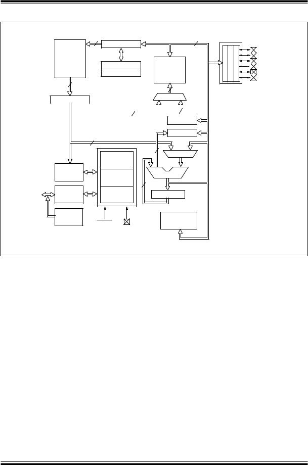
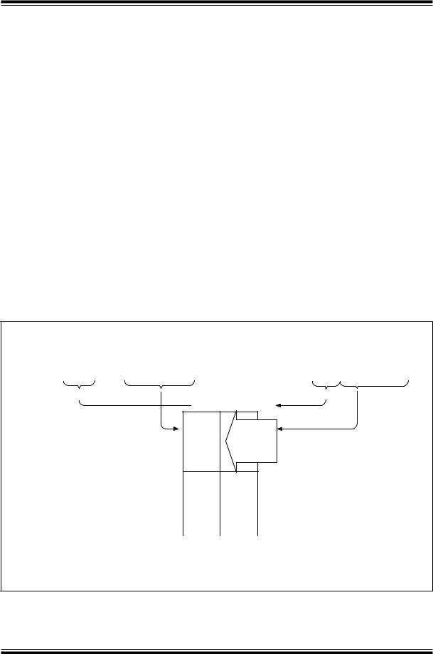
A simplified block diagram is shown in Figure 3-1, with the corresponding device pins described in Table 3-1.
1998 Microchip Technology Inc. |
DS40139D-page 9 |
PIC12C5XX |
|
|
|
|
|
|
FIGURE 3-1: PIC12C5XX BLOCK DIAGRAM |
|
|
|
|||
|
|
12 |
Data Bus |
8 |
GPIO |
|
|
EPROM |
Program Counter |
|
|
GP0 |
|
|
512 x 12 or |
|
|
|
|
|
|
|
|
|
|
GP1 |
|
|
1024 x 12 |
|
RAM |
|
||
|
Program |
|
|
GP2/T0CKI |
||
|
STACK1 |
25 x 8 or |
|
GP3/MCLR/Vpp |
||
|
Memory |
41 x 8 |
|
|||
|
STACK2 |
|
GP4/OSC2 |
|||
|
|
|
File |
|
||
|
|
|
|
|
GP5/OSC1/CLKIN |
|
Program |
|
|
Registers |
|
||
|
|
|
|
|||
12 |
|
RAM Addr |
9 |
|
|
|
Bus |
|
|
|
|
||
Instruction reg |
|
Addr MUX |
|
|
||
|
|
|
|
|
||
|
|
|
Direct Addr |
5 |
|
5-7 |
|
Indirect |
||
|
|
|
|
|
|
|
Addr |
|||
|
|
|
|
|
|
|
||||
|
|
|
|
|
|
|
|
|
|
|
FSR reg
|
|
8 |
|
STATUS reg |
|
|
|
|
|
|
|
|
3 |
MUX |
|
|
Device Reset |
|
|
|
|
|
|
|
|
Instruction |
Timer |
|
|
|
|
|
|
|
|
Decode & |
Power-on |
|
ALU |
|
Control |
|
||
|
Reset |
|
|
|
|
|
8 |
|
|
|
|
|
|
|
OSC1/CLKIN |
Timing |
Watchdog |
|
W reg |
OSC2 |
Generation |
Timer |
|
|
|
Internal RC |
|
|
|
|
OSC |
MCLR |
|
Timer0 |
|
|
|
|
|
|
|
Vdd, Vss |
|
|
DS40139D-page 10 |
1998 Microchip Technology Inc. |
|
|
|
|
|
|
|
|
PIC12C5XX |
||||||||
|
|
|
|
|
|
|
|
|
|
|
|
|
|
|
|
|
TABLE 3-1: |
PIC12C5XX PINOUT DESCRIPTION |
|
|
|
|
|
|
|
|
|
||||||
|
|
|
|
|
|
|
|
|
|
|
|
|
|
|
|
|
|
Name |
|
DIP |
SOIC |
I/O/P |
Buffer |
Description |
|||||||||
|
|
Pin # |
Pin # |
Type |
Type |
|||||||||||
|
|
|
|
|
|
|
|
|
|
|
|
|
||||
|
|
|
|
|
|
|
||||||||||
GP0 |
|
7 |
7 |
I/O |
TTL/ST |
Bi-directional I/O port/ serial programming data. Can |
||||||||||
|
|
|
|
|
|
|
|
be software programmed for internal weak pull-up and |
||||||||
|
|
|
|
|
|
|
|
wake-up from SLEEP on pin change. This buffer is a |
||||||||
|
|
|
|
|
|
|
|
Schmitt Trigger input when used in serial programming |
||||||||
|
|
|
|
|
|
|
|
mode. |
||||||||
GP1 |
|
6 |
6 |
I/O |
TTL/ST |
Bi-directional I/O port/ serial programming clock. Can |
||||||||||
|
|
|
|
|
|
|
|
be software programmed for internal weak pull-up and |
||||||||
|
|
|
|
|
|
|
|
wake-up from SLEEP on pin change. This buffer is a |
||||||||
|
|
|
|
|
|
|
|
Schmitt Trigger input when used in serial programming |
||||||||
|
|
|
|
|
|
|
|
mode. |
||||||||
GP2/T0CKI |
|
5 |
5 |
I/O |
ST |
Bi-directional I/O port. Can be configured as T0CKI. |
||||||||||
|
|
|
|
4 |
4 |
I |
TTL/ST |
Input port/master clear (reset) input/programming volt- |
||||||||
GP3/MCLR/V |
PP |
|
||||||||||||||
|
|
|
|
|
|
|
|
age input. When configured as |
MCLR, |
this pin is an |
||||||
|
|
|
|
|
|
|
|
active low reset to the device. Voltage on |
|
|
|
|
||||
|
|
|
|
|
|
|
|
MCLR/VPP |
||||||||
|
|
|
|
|
|
|
|
must not exceed VDD during normal device operation |
||||||||
|
|
|
|
|
|
|
|
or the device will enter programming mode. Can be |
||||||||
|
|
|
|
|
|
|
|
software programmed for internal weak pull-up and |
||||||||
|
|
|
|
|
|
|
|
wake-up from SLEEP on pin change. Weak pull-up |
||||||||
|
|
|
|
|
|
|
|
always on if configured as |
|
ST when in |
|
|
||||
|
|
|
|
|
|
|
|
MCLR. |
MCLR |
|||||||
|
|
|
|
|
|
|
|
mode. |
||||||||
GP4/OSC2 |
|
3 |
3 |
I/O |
TTL |
Bi-directional I/O port/oscillator crystal output. Con- |
||||||||||
|
|
|
|
|
|
|
|
nections to crystal or resonator in crystal oscillator |
||||||||
|
|
|
|
|
|
|
|
mode (XT and LP modes only, GPIO in other modes). |
||||||||
GP5/OSC1/CLKIN |
2 |
2 |
I/O |
TTL/ST |
Bidirectional IO port/oscillator crystal input/external |
|||||||||||
|
|
|
|
|
|
|
|
clock source input (GPIO in Internal RC mode only, |
||||||||
|
|
|
|
|
|
|
|
OSC1 in all other oscillator modes). TTL input when |
||||||||
|
|
|
|
|
|
|
|
GPIO, ST input in external RC oscillator mode. |
||||||||
VDD |
|
1 |
1 |
P |
— |
Positive supply for logic and I/O pins |
||||||||||
VSS |
|
8 |
8 |
P |
— |
Ground reference for logic and I/O pins |
||||||||||
Legend: I = input, O = output, I/O = input/output, P = power, — = not used, TTL = TTL input, ST = Schmitt Trigger input
1998 Microchip Technology Inc. |
DS40139D-page 11 |
PIC12C5XX
3.1Clocking Scheme/Instruction Cycle
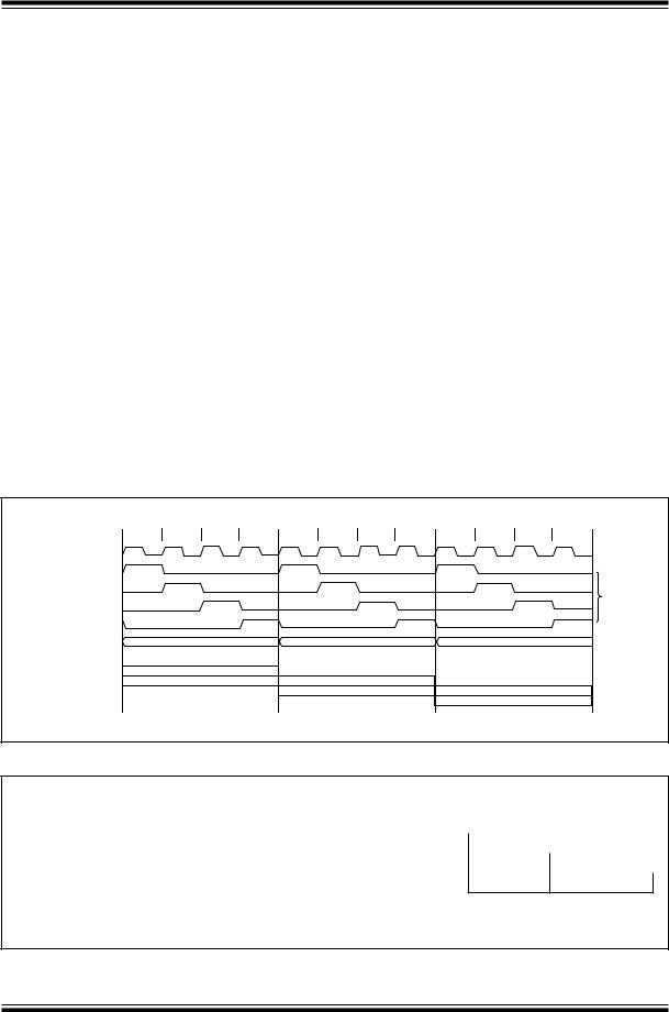
The clock input (OSC1/CLKIN pin) is internally divided by four to generate four non-overlapping quadrature clocks namely Q1, Q2, Q3 and Q4. Internally, the program counter is incremented every Q1, and the instruction is fetched from program memory and latched into instruction register in Q4. It is decoded and executed during the following Q1 through Q4. The clocks and instruction execution flow is shown in Figure 3-2 and Example 3-1.
3.2Instruction Flow/Pipelining
An Instruction Cycle consists of four Q cycles (Q1, Q2, Q3 and Q4). The instruction fetch and execute are pipelined such that fetch takes one instruction cycle while decode and execute takes another instruction cycle. However, due to the pipelining, each instruction effectively executes in one cycle. If an instruction causes the program counter to change (e.g., GOTO) then two cycles are required to complete the instruction (Example 3-1).
A fetch cycle begins with the program counter (PC) incrementing in Q1.
In the execution cycle, the fetched instruction is latched into the Instruction Register (IR) in cycle Q1. This instruction is then decoded and executed during the Q2, Q3, and Q4 cycles. Data memory is read during Q2 (operand read) and written during Q4 (destination write).
FIGURE 3-2: CLOCK/INSTRUCTION CYCLE
Q1 |
Q2 |
Q3 |
Q4 |
Q1 |
Q2 |
Q3 |
Q4 |
Q1 |
Q2 |
Q3 |
Q4 |
OSC1 |
|
|
|
|
|
|
|
|
|
|
|
Q1 |
|
|
|
|
|
|
|
|
|
|
|
Q2 |
|
|
|
|
|
|
|
|
|
|
Internal |
Q3 |
|
|
|
|
|
|
|
|
|
|
phase |
|
|
|
|
|
|
|
|
|
|
clock |
|
|
|
|
|
|
|
|
|
|
|
|
|
Q4 |
|
|
|
|
|
|
|
|
|
|
|
PC |
|
PC |
|
|
PC+1 |
|
|
|
|
PC+2 |
|
|
Fetch INST (PC) |
|
|
|
|
|
|
|
|
|
|
|
Execute INST (PC-1) |
|
|
Fetch INST (PC+1) |
|
|
|
|
|
||
|
|
|
|
|
Execute INST (PC) |
|
|
Fetch INST (PC+2) |
|
||
|
|
|
|
|
|
|
|
|
Execute INST (PC+1) |
|
|
EXAMPLE 3-1: INSTRUCTION PIPELINE FLOW
1. |
MOVLW |
03H |
Fetch 1 |
Execute 1 |
|
|
|
|
|
|
|
|
|
|
|
|
|
2. |
MOVWF |
GPIO |
|
Fetch 2 |
Execute 2 |
|
|
|
|
|
|
|
|
|
|
|
|
3. |
CALL |
SUB_1 |
|
|
Fetch 3 |
Execute 3 |
|
|
|
|
|
|
|
|
|
|
|
4. |
BSF |
GPIO, BIT1 |
|
|
|
Fetch 4 |
Flush |
|
|
|
|
|
|
|
|
|
|
Fetch SUB_1 Execute SUB_1
All instructions are single cycle, except for any program branches. These take two cycles since the fetch instruction is “flushed” from the pipeline while the new instruction is being fetched and then executed.
DS40139D-page 12 |
1998 Microchip Technology Inc. |
4.0MEMORY ORGANIZATION
PIC12C5XX memory is organized into program memory and data memory. For devices with more than 512 bytes of program memory, a paging scheme is used. Program memory pages are accessed using one STATUS register bit. For the PIC12C509(A) with a data memory register file of more than 32 registers, a banking scheme is used. Data memory banks are accessed using the File Select Register (FSR).
4.1Program Memory Organization
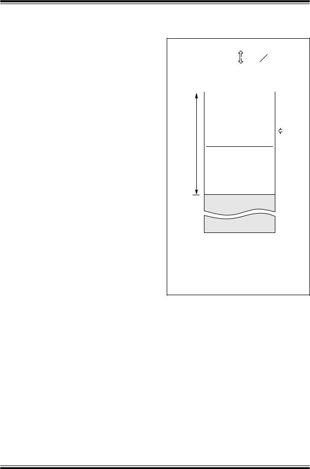
The PIC12C5XX devices have a 12-bit Program Counter (PC) capable of addressing a 2K x 12 program memory space.
Only the first 512 x 12 (0000h-01FFh) for the PIC12C508(A) and 1K x 12 (0000h-03FFh) for the PIC12C509(A) are physically implemented. Refer to Figure 4-1. Accessing a location above these boundaries will cause a wrap-around within the first 512 x 12 space (PIC12C508(A)) or 1K x 12 space (PIC12C509(A)). The effective reset vector is at 000h, (see Figure 4-1). Location 01FFh (PIC12C508(A)) or location 03FFh (PIC12C509(A)) contains the internal clock oscillator calibration value. This value should never be overwritten.
PIC12C5XX
FIGURE 4-1: PROGRAM MEMORY MAP AND STACK FOR THE PIC12C5XX
|
|
|
|
|
PC<11:0> |
|
|
||
CALL, RETLW |
12 |
|
|
|
|||||
|
|
|
|
|
|
|
|
|
|
|
|
|
|
|
Stack Level 1 |
|
|
||
|
|
|
|
|
Stack Level 2 |
|
|
||
|
|
|
|
|
|
|
|||
|
|
|
|
Reset Vector (note 1) |
0000h |
||||
|
|
|
|||||||
|
|
|
|
|
On-chip Program |
|
|
||
|
|
|
|
|
Memory |
|
|
||
MemoryUser Space |
|
512 Word (PIC12C508(A)) |
|
|
|||||
|
|
|
|||||||
|
01FFh |
||||||||
|
|
|
|
||||||
|
|
|
|
|
|
|
|
||
|
|
|
|
|
|
|
|
0200h |
|
|
|
|
|
|
On-chip Program |
|
|
||
|
|
|
|
|
Memory |
|
|
||
1024 Word (PIC12C509(A)) |
03FFh |
|
0400h |
|
7FFh |
Note 1: Address 0000h becomes the effective reset vector. Location 01FFh (PIC12C508(A)) or location 03FFh (PIC12C509(A)) contains the MOVLW XX INTERNAL RC oscillator calibration value.
1998 Microchip Technology Inc. |
DS40139D-page 13 |

PIC12C5XX
4.2Data Memory Organization
Data memory is composed of registers, or bytes of RAM. Therefore, data memory for a device is specified by its register file. The register file is divided into two functional groups: special function registers and general purpose registers.
The special function registers include the TMR0 register, the Program Counter (PC), the Status Register, the I/O registers (ports), and the File Select Register (FSR). In addition, special purpose registers are used to control the I/O port configuration and prescaler options.
The general purpose registers are used for data and control information under command of the instructions.
For the PIC12C508(A), the register file is composed of 7 special function registers and 25 general purpose registers (Figure 4-2).
For the PIC12C509(A), the register file is composed of 7 special function registers, 25 general purpose registers, and 16 general purpose registers that may be addressed using a banking scheme (Figure 4-3).
4.2.1GENERAL PURPOSE REGISTER FILE
The general purpose register file is accessed either directly or indirectly through the file select register FSR (Section 4.8).
FIGURE 4-2: |
PIC12C508(A) REGISTER FILE |
|||
|
MAP |
|
|
|
File Address |
|
|
||
|
|
|
|
|
|
00h |
|
INDF(1) |
|
|
01h |
|
TMR0 |
|
|
|
|
|
|
|
02h |
|
PCL |
|
|
03h |
|
STATUS |
|
|
|
|
|
|
|
04h |
|
FSR |
|
|
05h |
|
OSCCAL |
|
|
|
|
|
|
|
06h |
|
GPIO |
|
|
07h |
|
|
|
|
|
|
|
|
|
|
|
General |
|
|
|
|
Purpose |
|
|
|
|
Registers |
|
|
1Fh |
|
|
|
Note 1: |
Not a physical register. See Section 4.8 |
|||
|
|
|
|
|
FIGURE 4-3: PIC12C509(A) REGISTER FILE MAP
FSR<6:5> |
|
|
00 |
|
|
01 |
|
|
|
|||
|
|
|
|
|
|
|
||||||
File Address |
|
|
|
|
|
|
|
|
|
|
||
|
00h |
|
|
INDF(1) |
20h |
|
||||||
|
|
|
|
|||||||||
|
01h |
|
|
TMR0 |
|
|
|
|
|
|||
|
02h |
|
|
PCL |
|
|
|
|
|
|||
|
|
|
|
|
|
|
|
|
|
|
|
|
|
03h |
|
|
STATUS |
|
Addresses map |
|
|||||
|
|
|
|
back to |
|
|
||||||
|
04h |
|
|
FSR |
|
|
|
|||||
|
|
|
|
addresses |
|
|
||||||
|
05h |
|
|
OSCCAL |
|
in Bank 0. |
|
|
||||
|
06h |
|
|
GPIO |
|
|
|
|
|
|||
|
07h |
|
|
|
|
|
|
|
|
|
|
|
|
|
|
|
|
|
|
|
|
|
|
||
|
|
|
|
|
|
|
|
|
|
|
|
|
|
|
|
General |
|
|
|
|
|
||||
|
|
|
|
|
Purpose |
|
|
|
|
|
|
|
|
|
|
|
|
Registers |
|
|
2Fh |
|
|||
|
0Fh |
|
|
|
|
|
|
|||||
|
|
|
10h |
30h |
|
|||||||
|
|
|
|
|
|
|
|
General |
|
|
|
|
|
|
|
|
|
General |
|
||||||
|
|
|
|
|
Purpose |
|
|
Purpose |
|
|
|
|
|
|
|
|
|
Registers |
|
|
Registers |
|
|
|
|
|
|
|
1Fh |
3Fh |
|
|||||||
|
|
|
|
|
Bank 0 |
|
Bank 1 |
|
||||
|
Note 1: |
Not a physical register. See Section 4.8 |
|
|||||||||
|
|
|
|
|
|
|
|
|
|
|
|
|
|
|
|
|
|
|
|
|
|
|
|
|
|
|
|
|
|
|
|
|
|
|
|
|
|
|
DS40139D-page 14 |
1998 Microchip Technology Inc. |

PIC12C5XX
4.2.2SPECIAL FUNCTION REGISTERS
The Special Function Registers (SFRs) are registers used by the CPU and peripheral functions to control the operation of the device (Table 4-1).
The special registers can be classified into two sets. The special function registers associated with the “core”functions are described in this section. Those related to the operation of the peripheral features are described in the section for each peripheral feature.
TABLE 4-1: |
SPECIAL FUNCTION REGISTER (SFR) SUMMARY |
|
|
|
||||||||||||||
|
|
|
|
|
|
|
|
|
|
|
|
|
|
|
|
|
|
|
|
|
|
|
|
|
|
|
|
|
|
|
|
|
|
|
|
Value on |
Value on |
|
|
|
|
|
|
|
|
|
|
|
|
|
|
|
|
|
Power-On |
All Other |
Address |
Name |
Bit 7 |
Bit 6 |
|
Bit 5 |
Bit 4 |
Bit 3 |
|
Bit 2 |
Bit 1 |
Bit 0 |
Reset |
Resets(2) |
|||||
|
|
|
|
|
|
|
|
|
|
|
|
|
|
|
|
|
||
N/A |
TRIS |
|
I/O control registers |
|
|
|
|
|
|
|
|
|
|
|
--11 1111 |
--11 1111 |
||
|
|
|
|
|
|
|
|
|
||||||||||
|
|
|
Contains control bits to configure Timer0, Timer0/WDT |
|
|
|
1111 1111 |
1111 1111 |
||||||||||
N/A |
OPTION |
prescaler, wake-up on change, and weak pull-ups |
|
|
|
|||||||||||||
|
|
|
|
|
|
|
||||||||||||
00h |
INDF |
|
Uses contents of FSR to address data memory (not a physical register) |
|
xxxx xxxx |
uuuu uuuu |
||||||||||||
|
|
|
|
|
|
|
|
|
|
|
|
|
|
|
|
|||
01h |
TMR0 |
|
8-bit real-time clock/counter |
|
|
|
|
|
|
|
|
|
|
xxxx xxxx |
uuuu uuuu |
|||
|
|
|
|
|
|
|
|
|
|
|
|
|
|
|
|
|
||
02h(1) |
PCL |
|
Low order 8 bits of PC |
|
|
|
|
|
|
|
|
|
|
|
1111 1111 |
1111 1111 |
||
03h |
STATUS |
|
GPWUF |
— |
|
PA0 |
|
|
|
|
|
|
|
Z |
DC |
C |
0001 1xxx |
q00q quuu(3) |
|
|
TO |
PD |
|||||||||||||||
|
FSR |
|
|
|
|
|
|
|
|
|
|
|
|
|
|
|
|
|
04h |
(12C508/ |
Indirect data memory address pointer |
|
|
|
|
|
|
|
111x xxxx |
111u uuuu |
|||||||
12C508A) |
|
|
|
|
|
|
|
|||||||||||
|
|
|
|
|
|
|
|
|
|
|
|
|
|
|
|
|
|
|
|
FSR |
|
|
|
|
|
|
|
|
|
|
|
|
|
|
|
|
|
04h |
(12C509/ |
Indirect data memory address pointer |
|
|
|
|
|
|
|
110x xxxx |
11uu uuuu |
|||||||
12C509A) |
|
|
|
|
|
|
|
|||||||||||
|
|
|
|
|
|
|
|
|
|
|
|
|
|
|
|
|
|
|
|
OSCCAL |
|
|
|
|
|
|
|
|
|
|
|
|
|
|
|
|
|
|
(12C508/ |
|
|
|
|
|
|
|
|
|
|
|
|
|
|
0111 ---- |
uuuu ---- |
|
05h |
12C509) |
CAL3 |
CAL2 |
|
CAL1 |
CAL0 |
|
— |
|
— |
— |
— |
||||||
|
|
|
|
|
|
|
|
|
|
|
|
|
|
|
|
|
|
|
|
OSCCAL |
|
|
|
|
|
|
|
|
|
|
|
|
|
|
|
|
|
|
(12C508A/ |
|
|
|
|
|
|
|
|
|
|
|
|
|
|
|
|
|
05h |
12C509A) |
CAL5 |
CAL4 |
|
CAL3 |
CAL2 |
CAL1 |
|
CAL0 |
— |
— |
1000 00-- |
uuuu uu-- |
|||||
|
|
|
|
|||||||||||||||
|
|
|
|
|
|
|
|
|
|
|
|
|
|
|
||||
06h |
GPIO |
|
— |
— |
|
GP5 |
GP4 |
GP3 |
|
GP2 |
GP1 |
GP0 |
--xx xxxx |
--uu uuuu |
||||
|
|
|
|
|
|
|
|
|
|
|
|
|
|
|
|
|
|
|
Legend: Shaded boxes = unimplemented or unused, — = unimplemented, read as '0' (if applicable) x = unknown, u = unchanged, q = see the tables in Section 7.7 for possible values.
Note 1: The upper byte of the Program Counter is not directly accessible. See Section 4.6 for an explanation of how to access these bits.
2:Other (non power-up) resets include external reset through MCLR, watchdog timer and wake-up on pin change reset.
3:If reset was due to wake-up on pin change then bit 7 = 1. All other resets will cause bit 7 = 0.
1998 Microchip Technology Inc. |
DS40139D-page 15 |

PIC12C5XX
4.3STATUS Register
This register contains the arithmetic status of the ALU, the RESET status, and the page preselect bit for program memories larger than 512 words.
The STATUS register can be the destination for any instruction, as with any other register. If the STATUS register is the destination for an instruction that affects the Z, DC or C bits, then the write to these three bits is disabled. These bits are set or cleared according to the device logic. Furthermore, the TO and PD bits are not writable. Therefore, the result of an instruction with the STATUS register as destination may be different than intended.
For example, CLRF STATUS will clear the upper three bits and set the Z bit. This leaves the STATUS register as 000u u1uu (where u = unchanged).
It is recommended, therefore, that only BCF, BSF and MOVWF instructions be used to alter the STATUS register because these instructions do not affect the Z, DC or C bits from the STATUS register. For other instructions, which do affect STATUS bits, see Instruction Set Summary.
FIGURE 4-4: STATUS REGISTER (ADDRESS:03h)
|
R/W-0 |
|
R/W-0 |
R/W-0 |
R-1 |
R-1 |
R/W-x |
R/W-x |
R/W-x |
|
|
|
||||||||||||||
|
GPWUF |
|
|
|
— |
PA0 |
|
|
TO |
|
|
|
PD |
|
Z |
|
DC |
C |
|
R = Readable bit |
|
|||||
|
bit7 |
|
|
6 |
|
5 |
|
|
4 |
|
|
3 |
|
2 |
|
1 |
bit0 |
|
W = Writable bit |
|
||||||
|
|
|
|
|
|
|
|
|
|
|
- n = Value at POR reset |
|
||||||||||||||
|
|
|
|
|
|
|
|
|
|
|
|
|
|
|
|
|
|
|
|
|
|
|
|
|
|
|
|
bit 7: |
GPWUF: GPIO reset bit |
|
|
|
|
|
|
|
|
|
|
|
|
|
|
||||||||||
|
|
|
1 |
= Reset due to wake-up from SLEEP on pin change |
|
|
|
|
|
|||||||||||||||||
|
|
|
0 |
= After power up or other reset |
|
|
|
|
|
|
|
|
|
|
||||||||||||
|
bit |
6: |
Unimplemented |
|
|
|
|
|
|
|
|
|
|
|
|
|
|
|||||||||
|
bit |
5: |
PA0: Program page preselect bits |
|
|
|
|
|
|
|
|
|
|
|||||||||||||
|
|
|
1 |
= Page 1 (200h - 3FFh) - PIC12C509(A) |
|
|
|
|
|
|
|
|||||||||||||||
|
|
|
0 |
= Page 0 (000h - 1FFh) - PIC12C508(A) and PIC12C509(A) |
|
|
|
|
||||||||||||||||||
|
|
|
Each page is 512 bytes. |
|
|
|
|
|
|
|
|
|
|
|
|
|
|
|||||||||
|
|
|
Using the PA0 bit as a general purpose read/write bit in devices which do not use it for program |
|
||||||||||||||||||||||
|
|
|
page preselect is not recommended since this may affect upward compatibility with future products. |
|
||||||||||||||||||||||
|
bit |
4: |
|
: Time-out bit |
|
|
|
|
|
|
|
|
|
|
|
|
|
|
||||||||
|
TO |
|
|
|
|
|
|
|
|
|
|
|
|
|
|
|||||||||||
|
|
|
1 |
= After power-up, CLRWDT instruction, or SLEEP instruction |
|
|
|
|
||||||||||||||||||
|
|
|
0 |
= A WDT time-out occurred |
|
|
|
|
|
|
|
|
|
|
||||||||||||
|
bit |
3: |
|
: Power-down bit |
|
|
|
|
|
|
|
|
|
|
|
|
|
|
||||||||
|
PD |
|
|
|
|
|
|
|
|
|
|
|
|
|
|
|||||||||||
|
|
|
1 |
= After power-up or by the CLRWDT instruction |
|
|
|
|
|
|||||||||||||||||
|
|
|
0 |
= By execution of the SLEEP instruction |
|
|
|
|
|
|
|
|||||||||||||||
|
bit |
2: |
Z: Zero bit |
|
|
|
|
|
|
|
|
|
|
|
|
|
|
|
|
|
|
|
||||
|
|
|
1 |
= The result of an arithmetic or logic operation is zero |
|
|
|
|
|
|||||||||||||||||
|
|
|
0 |
= The result of an arithmetic or logic operation is not zero |
|
|
|
|
|
|||||||||||||||||
|
bit |
1: |
|
|
|
|
|
|
bit (for ADDWF and SUBWF instructions) |
|
|
|
|
|||||||||||||
|
DC: Digit carry/borrow |
|
|
|
|
|||||||||||||||||||||
|
|
|
ADDWF |
|
|
|
|
|
|
|
|
|
|
|
|
|
|
|
|
|
|
|
||||
|
|
|
1 |
= A carry from the 4th low order bit of the result occurred |
|
|
|
|
|
|||||||||||||||||
|
|
|
0 |
= A carry from the 4th low order bit of the result did not occur |
|
|
|
|
||||||||||||||||||
|
|
|
SUBWF |
|
|
|
|
|
|
|
|
|
|
|
|
|
|
|
|
|
|
|
||||
|
|
|
1 |
= A borrow from the 4th low order bit of the result did not occur |
|
|
|
|
||||||||||||||||||
|
|
|
0 |
= A borrow from the 4th low order bit of the result occurred |
|
|
|
|
||||||||||||||||||
|
bit |
0: |
|
|
|
bit (for ADDWF, SUBWF and RRF, RLF instructions) |
|
|
|
|
||||||||||||||||
|
C: Carry/borrow |
|
|
|
|
|||||||||||||||||||||
|
|
|
ADDWF |
|
|
|
|
|
|
|
|
|
SUBWF |
|
|
|
RRF or RLF |
|
||||||||
|
|
|
1 |
= A carry occurred |
|
|
|
|
1 = A borrow did not occur |
Load bit with LSB or MSB, respectively |
|
|||||||||||||||
|
|
|
0 |
= A carry did not occur |
|
|
|
|
0 = A borrow occurred |
|
|
|
|
|
||||||||||||
|
|
|
|
|
|
|
|
|
|
|
|
|
|
|
|
|
|
|
|
|
|
|
|
|
|
|
DS40139D-page 16 |
1998 Microchip Technology Inc. |

PIC12C5XX
4.4OPTION Register
The OPTION register is a 8-bit wide, write-only register which contains various control bits to configure the Timer0/WDT prescaler and Timer0.
By executing the OPTION instruction, the contents of the W register will be transferred to the OPTION register. A RESET sets the OPTION<7:0> bits.
FIGURE 4-5: OPTION REGISTER
Note: If TRIS bit is set to ‘0’, the wake-up on change and pull-up functions are disabled for that pin; i.e., note that TRIS overrides OPTION control of GPPU and GPWU.
Note: If the T0CS bit is set to ‘1’, GP2 is forced to be an input even if TRIS GP2 = ‘0’.
|
W-1 |
|
|
|
W-1 |
W-1 |
W-1 |
W-1 |
W-1 |
W-1 |
W-1 |
|
|
|
||||
|
GPWU |
|
|
|
GPPU |
|
|
T0CS |
T0SE |
PSA |
PS2 |
|
PS1 |
PS0 |
|
W |
= Writable bit |
|
bit7 |
|
|
6 |
|
|
|
5 |
4 |
3 |
2 |
|
1 |
bit0 |
|
U |
= Unimplemented bit |
||
|
|
|
|
|
|
|
|
|
|
|
|
|
|
|
|
|
- n = Value at POR reset |
|
|
|
|
|
|
|
|
|
|
|
|
|
|
|
|
|
|
Reference Table 4-1 for |
|
|
|
|
|
|
|
|
|
|
|
|
|
|
|
|
|
|
other resets. |
|
bit 7: |
|
|
|
|
Enable wake-up on pin change (GP0, GP1, GP3) |
|
|
|
|
|
||||||||
GPWU: |
|
|
|
|
|
|||||||||||||
|
|
1 |
= Disabled |
|
|
|
|
|
|
|
|
|
|
|||||
|
|
0 |
= Enabled |
|
|
|
|
|
|
|
|
|
|
|||||
bit 6: GPPU: Enable weak pull-ups (GP0, GP1, GP3) 1 = Disabled
0 = Enabled
bit 5: T0CS: Timer0 clock source select bit 1 = Transition on T0CKI pin
0 = Transition on internal instruction cycle clock, Fosc/4
bit |
4: |
T0SE: Timer0 source edge select bit |
||||||
|
|
1 |
= Increment on high to low transition on the T0CKI pin |
|||||
|
|
0 |
= Increment on low to high transition on the T0CKI pin |
|||||
bit |
3: |
PSA: Prescaler assignment bit |
|
|
||||
|
|
1 |
= Prescaler assigned to the WDT |
|||||
|
|
0 |
= Prescaler assigned to Timer0 |
|
|
|||
bit |
2-0: |
PS2:PS0: Prescaler rate select bits |
||||||
|
|
|
Bit Value |
Timer0 Rate |
WDT Rate |
|||
|
|
|
|
|
|
|
|
|
|
|
|
000 |
1 |
: 2 |
1 : |
1 |
|
|
|
|
001 |
1 |
: 4 |
1 : |
2 |
|
|
|
|
010 |
1 |
: 8 |
1 : |
4 |
|
|
|
|
011 |
1 |
: 16 |
1 : |
8 |
|
|
|
|
100 |
1 |
: 32 |
1 : |
16 |
|
|
|
|
101 |
1 |
: 64 |
1 : |
32 |
|
|
|
|
110 |
1 |
: 128 |
1 : |
64 |
|
|
|
|
111 |
1 |
: 256 |
1 : |
128 |
|
1998 Microchip Technology Inc. |
DS40139D-page 17 |

PIC12C5XX
4.5OSCCAL Register
The Oscillator Calibration (OSCCAL) register is used to calibrate the internal 4 MHz oscillator. It contains four to six bits for calibration. Increasing the cal value increases the frequency. See Section 7.2.5 for more information on the internal oscillator.
FIGURE 4-6: OSCCAL REGISTER (ADDRESS 8Fh)
R/W-0 |
R/W-1 |
R/W-1 |
R/W-1 |
R/W-0 |
R/W-0 |
U-0 |
U-0 |
|
|
|
CAL3 |
CAL2 |
CAL1 |
CAL0 |
— |
— |
— |
— |
|
R |
= Readable bit |
bit7 |
|
|
|
|
|
|
bit0 |
|
W |
= Writable bit |
|
|
|
|
|
|
|
|
|
U |
= Unimplemented bit, |
|
|
|
|
|
|
|
|
|
|
read as ‘0’ |
|
|
|
|
|
|
|
|
|
- n |
= Value at POR reset |
bit 7-4: |
CAL<3:0>: Calibration |
|
|
|
|
|
|
|
||
bit 3-0: |
Unimplemented: Read as '0' |
|
|
|
|
|
|
|||
FIGURE 4-7: OSCCAL REGISTER (ADDRESS 8Fh)PIC12C508A/C509A
R/W-1 |
R/W-0 |
R/W-0 |
R/W-0 |
R/W-0 |
R/W-0 |
U-0 |
U-0 |
|
|
|
|
CAL5 |
CAL4 |
CAL3 |
CAL2 |
CAL1 |
CAL0 |
— |
— |
|
|
R |
= Readable bit |
bit7 |
|
|
|
|
|
|
bit0 |
|
|
W |
= Writable bit |
|
|
|
|
|
|
|
|
|
|
U |
= Unimplemented bit, |
|
|
|
|
|
|
|
|
|
|
|
read as ‘0’ |
|
|
|
|
|
|
|
|
|
|
- n |
= Value at POR reset |
bit 7-2: CAL<5:0>: Calibration
bit 1-0: Unimplemented: Read as '0'
DS40139D-page 18 |
1998 Microchip Technology Inc. |
PIC12C5XX
4.6Program Counter
As a program instruction is executed, the Program Counter (PC) will contain the address of the next program instruction to be executed. The PC value is increased by one every instruction cycle, unless an instruction changes the PC.
For a GOTO instruction, bits 8:0 of the PC are provided by the GOTO instruction word. The PC Latch (PCL) is mapped to PC<7:0>. Bit 5 of the STATUS register provides page information to bit 9 of the PC (Figure 4- 8).
For a CALL instruction, or any instruction where the PCL is the destination, bits 7:0 of the PC again are provided by the instruction word. However, PC<8> does not come from the instruction word, but is always cleared (Figure 4-8).
Instructions where the PCL is the destination, or Modify PCL instructions, include MOVWF PC, ADDWF PC, and BSF PC,5.
Note: Because PC<8> is cleared in the CALL instruction, or any Modify PCL instruction, all subroutine calls or computed jumps are limited to the first 256 locations of any program memory page (512 words long).
FIGURE 4-8: LOADING OF PC
BRANCH INSTRUCTIONS - PIC12C5XX
GOTO Instruction
11 |
10 |
9 |
8 |
|
7 |
|
|
|
0 |
|||||
PC |
|
|
|
|
|
|
|
|
|
|
|
PCL |
|
|
|
|
|
|
|
|
|
|
|
|
|
|
|||
|
|
|
|
|
|
|
|
|
|
|
|
|
|
|
|
|
|
|
|
|
|
|
|
Instruction Word |
|
||||
|
|
|
|
|
|
|
PA0 |
|
|
|
|
|
|
|
|
|
|
7 |
|
|
|
|
|
0 |
|
|
|||
|
|
|
|
|
|
|
|
|
|
|
|
|
|
|
|
|
|
|
|
|
|
|
|
|
|
|
|
|
|
STATUS
CALL or Modify PCL Instruction
11 |
10 |
9 |
8 |
|
7 |
|
|
|
0 |
|||||
PC |
|
|
|
|
|
|
|
|
|
|
|
PCL |
|
|
|
|
|
|
|
|
|
|
|
|
|
|
|
||
|
|
|
|
|
|
|
|
|
|
|
|
|
|
|
|
|
|
|
|
|
|
|
|
|
Instruction Word |
|
|||
|
|
|
|
|
|
|
Reset to ‘0’ |
|
||||||
|
|
|
7 |
|
|
|
PA0 |
0 |
|
|
||||
|
|
|
|
|
|
|
|
|
|
|||||
|
|
|
|
|
|
|
|
|
|
|
|
|
|
|
|
|
|
|
|
|
|
|
|
|
|
|
|
|
|
STATUS
4.6.1EFFECTS OF RESET
The Program Counter is set upon a RESET, which means that the PC addresses the last location in the last page i.e., the oscillator calibration instruction. After executing MOVLW XX, the PC will roll over to location 00h, and begin executing user code.
The STATUS register page preselect bits are cleared upon a RESET, which means that page 0 is preselected.
Therefore, upon a RESET, a GOTO instruction will automatically cause the program to jump to page 0 until the value of the page bits is altered.
4.7Stack
PIC12C5XX devices have a 12-bit wide L.I.F.O. hardware push/pop stack.
A CALL instruction will push the current value of stack 1 into stack 2 and then push the current program counter value, incremented by one, into stack level 1. If more than two sequential CALL’s are executed, only the most recent two return addresses are stored.
A RETLW instruction will pop the contents of stack level 1 into the program counter and then copy stack level 2 contents into level 1. If more than two sequential RETLW’s are executed, the stack will be filled with the address previously stored in level 2. Note that the W register will be loaded with the literal value specified in the instruction. This is particularly useful for the implementation of data look-up tables within the program memory.
Upon any reset, the contents of the stack remain unchanged, however the program counter (PCL) will also be reset to 0.
Note 1: There are no STATUS bits to indicate stack overflows or stack underflow conditions.
Note 2: There are no instructions mnemonics called PUSH or POP. These are actions that occur from the execution of the CALL and RETLW instructions.
1998 Microchip Technology Inc. |
DS40139D-page 19 |
PIC12C5XX
4.8Indirect Data Addressing; INDF and FSR Registers
The INDF register is not a physical register. Addressing INDF actually addresses the register whose address is contained in the FSR register (FSR is a pointer). This is indirect addressing.
EXAMPLE 4-1: INDIRECT ADDRESSING
•Register file 07 contains the value 10h
•Register file 08 contains the value 0Ah
•Load the value 07 into the FSR register
•A read of the INDF register will return the value of 10h
•Increment the value of the FSR register by one (FSR = 08)
•A read of the INDR register now will return the value of 0Ah.
Reading INDF itself indirectly (FSR = 0) will produce 00h. Writing to the INDF register indirectly results in a no-operation (although STATUS bits may be affected).
A simple program to clear RAM locations 10h-1Fh using indirect addressing is shown in Example 4-2.
EXAMPLE 4-2: HOW TO CLEAR RAM USING INDIRECT ADDRESSING
|
movlw |
0x10 |
;initialize pointer |
|
movwf |
FSR |
; to RAM |
NEXT |
clrf |
INDF |
;clear INDF register |
|
incf |
FSR,F |
;inc pointer |
|
btfsc |
FSR,4 |
;all done? |
|
goto |
NEXT |
;NO, clear next |
CONTINUE |
|
|
|
|
: |
|
;YES, continue |
The FSR is a 5-bit wide register. It is used in conjunction with the INDF register to indirectly address the data memory area.
The FSR<4:0> bits are used to select data memory addresses 00h to 1Fh.
PIC12C508(A): Does not use banking. FSR<7:5> are unimplemented and read as '1's.
PIC12C509(A): Uses FSR<5>. Selects between bank 0 and bank 1. FSR<7:6> is unimplemented, read as '1’
.
FIGURE 4-9: DIRECT/INDIRECT ADDRESSING
|
|
|
|
Direct Addressing |
|
Indirect Addressing |
|
|||||||||||||
|
|
(FSR) |
|
|
|
|
|
|
|
|
|
|
|
|
|
|
|
|
||
6 5 |
|
|
|
4 (opcode) 0 |
6 5 4 |
(FSR) |
0 |
|||||||||||||
|
|
|
|
|
|
|
|
|
|
|
|
|
|
|
|
|
|
|
|
|
|
|
|
|
|
|
|
|
|
bank |
location select |
||||||||||
location select |
|
|
||||||||||||||||||
bank select |
|
|
|
|
|
|
||||||||||||||
|
|
|
|
|
|
|
||||||||||||||
|
|
|
|
|
|
|
|
|
|
|
|
|
|
|
|
|
|
|
|
|
 00 01
00 01
00h
Addresses map back to addresses in Bank 0.
Data 0Fh
Memory(1) 10h
1Fh |
3Fh |
Bank 0 |
Bank 1(2) |
Note 1: For register map detail see Section 4.2.
Note 2: PIC12C509(A) only
DS40139D-page 20 |
1998 Microchip Technology Inc. |
PIC12C5XX
5.0I/O PORT
As with any other register, the I/O register can be written and read under program control. However, read instructions (e.g., MOVF GPIO,W) always read the I/O pins independent of the pin’s input/output modes. On RESET, all I/O ports are defined as input (inputs are at hi-impedance) since the I/O control registers are all set.
5.1GPIO
GPIO is an 8-bit I/O register. Only the low order 6 bits are used (GP5:GP0). Bits 7 and 6 are unimplemented and read as '0's.Please note that GP3 is an input only pin. The configuration word can set several I/O’s to alternate functions. When acting as alternate functions the pins will read as ‘0’ during port read. Pins GP0, GP1, and GP3 can be configured with weak pull-ups and also with wake-up on change. The wake-up on change and weak pull-up functions are not pin selectable. If pin 4 is configured as MCLR, weak pullup is always on and wake-up on change for this pin is not enabled.
5.2TRIS Register
The output driver control register is loaded with the contents of the W register by executing the TRIS f instruction. A '1' from TRISa register bit puts the corresponding output driver in a hi-impedance mode.
A '0' puts the contents of the output data latch on the selected pins, enabling the output buffer. The exceptions are GP3 which is input only and GP2 which may be controlled by the option register, see Figure 4- 5.
Note: A read of the ports reads the pins, not the output data latches. That is, if an output driver on a pin is enabled and driven high, but the external system is holding it low, a read of the port will indicate that the pin is low.
The TRIS registers are “write-only” and are set (output drivers disabled) upon RESET.
TABLE 5-1: SUMMARY OF PORT REGISTERS
5.3I/O Interfacing
The equivalent circuit for an I/O port pin is shown in Figure 5-1. All port pins, except GP3 which is input only, may be used for both input and output operations. For input operations these ports are nonlatching. Any input must be present until read by an input instruction (e.g., MOVF GPIO,W). The outputs are latched and remain unchanged until the output latch is rewritten. To use a port pin as output, the corresponding direction control bit in TRIS must be cleared (= 0). For use as an input, the corresponding TRIS bit must be set. Any I/O pin (except GP3) can be programmed individually as input or output.
FIGURE 5-1: EQUIVALENT CIRCUIT FOR A SINGLE I/O PIN
Data |
|
|
|
Bus |
D |
Q |
|
|
|
||
WR |
Data |
VDD |
|
Latch |
|
||
|
|
||
Port |
CK |
Q |
|
|
|
||
|
|
P |
|
W |
|
N |
I/O |
Reg |
D |
Q |
pin(1) |
|
|
||
|
TRIS |
VSS |
|
|
Latch |
|
|
TRIS ‘f’ |
|
|
|
CK |
Q |
|
|
|
|
||
|
Reset |
(2) |
|
|
|
|
RD Port
Note 1: I/O pins have protection diodes to VDD and VSS. 2: See Table 3-1 for buffer type.
|
|
|
|
|
|
|
|
|
|
|
|
|
|
|
|
|
|
|
Value on |
|
|
|
|
|
|
|
|
|
|
|
|
|
|
|
|
|
|
|
|
|
Power-On |
Value on |
|
Address |
Name |
|
Bit 7 |
|
Bit 6 |
|
Bit 5 |
Bit 4 |
Bit 3 |
Bit 2 |
Bit 1 |
Bit 0 |
Reset |
All Other Resets |
|||||||
|
|
|
|
|
|
|
|
|
|
|
|
|
|
|
|
|
|
||||
|
|
|
|
|
|
|
|
|
|
|
|
|
|
|
|
||||||
N/A |
TRIS |
I/O control registers |
|
|
|
|
|
|
|
|
|
|
--11 |
1111 |
--11 1111 |
||||||
|
|
|
|
|
|
|
|
|
|
|
|
|
|
|
|
|
|
|
|
|
|
|
OPTION |
|
|
|
|
|
|
|
T0CS |
T0SE |
PSA |
PS2 |
PS1 |
PS0 |
|
|
|
||||
N/A |
|
GPWU |
GPPU |
1111 |
1111 |
1111 1111 |
|||||||||||||||
|
|
|
|
|
|
|
|
|
|
|
|
|
|
|
|
|
|
|
|||
03H |
STATUS |
GPWUF |
|
— |
|
PAO |
|
TO |
|
|
PD |
|
Z |
DC |
C |
0001 |
1xxx |
q00q quuu(1) |
|||
06h |
GPIO |
|
— |
|
— |
|
GP5 |
GP4 |
GP3 |
GP2 |
GP1 |
GP0 |
--xx xxxx |
--uu uuuu |
|||||||
|
|
|
|
|
|
|
|
|
|
|
|
|
|
|
|
|
|
|
|
|
|
Legend: Shaded cells not used by Port Registers, read as ‘0’, — = unimplemented, read as '0',x = unknown, u = unchanged, q = see tables in Section 7.7 for possible values.
Note 1: If reset was due to wake-up on change, then bit 7 = 1. All other resets will cause bit 7 = 0.
1998 Microchip Technology Inc. |
DS40139D-page 21 |
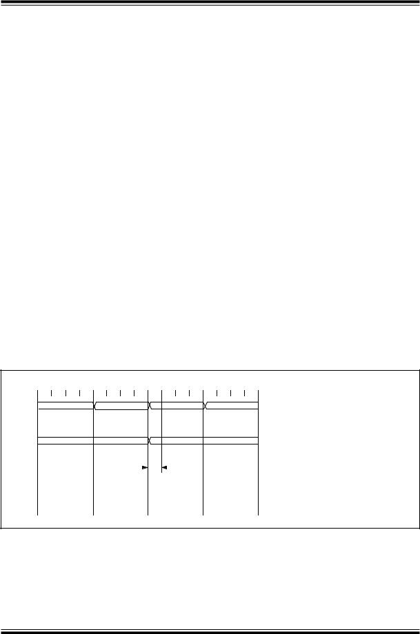
PIC12C5XX
5.4I/O Programming Considerations
5.4.1BI-DIRECTIONAL I/O PORTS
Some instructions operate internally as read followed by write operations. The BCF and BSF instructions, for example, read the entire port into the CPU, execute the bit operation and re-write the result. Caution must be used when these instructions are applied to a port where one or more pins are used as input/outputs. For example, a BSF operation on bit5 of GPIO will cause all eight bits of GPIO to be read into the CPU, bit5 to be set and the GPIO value to be written to the output latches. If another bit of GPIO is used as a bidirectional I/O pin (say bit0) and it is defined as an input at this time, the input signal present on the pin itself would be read into the CPU and rewritten to the data latch of this particular pin, overwriting the previous content. As long as the pin stays in the input mode, no problem occurs. However, if bit0 is switched into output mode later on, the content of the data latch may now be unknown.
Example 5-1 shows the effect of two sequential read- modify-write instructions (e.g., BCF, BSF, etc.) on an I/ O port.
A pin actively outputting a high or a low should not be driven from external devices at the same time in order to change the level on this pin (“wired-or”,“wired-and”). The resulting high output currents may damage the chip.
EXAMPLE 5-1: READ-MODIFY-WRITE INSTRUCTIONS ON AN I/O PORT
;Initial GPIO Settings
;GPIO<5:3> Inputs
;GPIO<2:0> Outputs
; |
|
GPIO latch |
GPIO pins |
||
; |
|
---------- |
---------- |
||
BCF |
GPIO, 5 |
;--01 |
-ppp |
--11 |
pppp |
BCF |
GPIO, 4 |
;--10 |
-ppp |
--11 |
pppp |
MOVLW |
007h |
; |
|
|
|
TRIS |
GPIO |
;--10 |
-ppp |
--11 |
pppp |
; |
|
|
|
|
|
;Note that the user may |
have expected the pin |
||||
;values |
to be --00 pppp. The 2nd BCF caused |
||||
;GP5 to |
be latched as the pin value (High). |
||||
5.4.2SUCCESSIVE OPERATIONS ON I/O PORTS
The actual write to an I/O port happens at the end of an instruction cycle, whereas for reading, the data must be valid at the beginning of the instruction cycle (Figure 5-2). Therefore, care must be exercised if a write followed by a read operation is carried out on the same I/O port. The sequence of instructions should allow the pin voltage to stabilize (load dependent) before the next instruction, which causes that file to be read into the CPU, is executed. Otherwise, the previous state of that pin may be read into the CPU rather than the new state. When in doubt, it is better to separate these instructions with a NOP or another instruction not accessing this I/O port.
FIGURE 5-2: SUCCESSIVE I/O OPERATION
Q1 Q2 Q3 Q4 Q1 Q2 Q3 Q4 Q1 Q2 Q3 Q4 Q1 Q2 Q3 Q4
Instruction |
PC |
|
PC + 1 |
|
PC + 2 |
PC + 3 |
|
|
|
|
|
|
|
|
|
fetched |
MOVWF GPIO |
MOVF GPIO,W |
|
NOP |
NOP |
||
|
|
||||||
GP5:GP0 |
|
|
|
|
|
|
|
|
|
Port pin |
Port pin |
|
|||
|
|
written here |
sampled here |
|
|||
Instruction |
|
|
|
|
|
|
|
executed |
|
MOVWF GPIO |
MOVF GPIO,W |
NOP |
|||
|
|
||||||
|
|
(Write to |
(Read |
|
|||
|
|
GPIO) |
GPIO) |
|
|||
This example shows a write to GPIO followed by a read from GPIO.
Data setup time = (0.25 TCY – TPD)
where: TCY = instruction cycle.
TPD = propagation delay
Therefore, at higher clock frequencies, a write followed by a read may be problematic.
DS40139D-page 22 |
1998 Microchip Technology Inc. |
PIC12C5XX
6.0TIMER0 MODULE AND TMR0 REGISTER
The Timer0 module has the following features:
•8-bit timer/counter register, TMR0
-Readable and writable
•8-bit software programmable prescaler
•Internal or external clock select
-Edge select for external clock
Figure 6-1 is a simplified block diagram of the Timer0 module.
Timer mode is selected by clearing the T0CS bit (OPTION<5>). In timer mode, the Timer0 module will increment every instruction cycle (without prescaler). If TMR0 register is written, the increment is inhibited for the following two instruction cycles (Figure 6-2 and Figure 6-3). The user can work around this by writing an adjusted value to the TMR0 register.
FIGURE 6-1: TIMER0 BLOCK DIAGRAM
Counter mode is selected by setting the T0CS bit (OPTION<5>). In this mode, Timer0 will increment either on every rising or falling edge of pin T0CKI. The T0SE bit (OPTION<4>) determines the source edge. Clearing the T0SE bit selects the rising edge. Restrictions on the external clock input are discussed in detail in Section 6.1.
The prescaler may be used by either the Timer0 module or the Watchdog Timer, but not both. The prescaler assignment is controlled in software by the control bit PSA (OPTION<3>). Clearing the PSA bit will assign the prescaler to Timer0. The prescaler is not readable or writable. When the prescaler is assigned to the Timer0 module, prescale values of 1:2, 1:4,..., 1:256 are selectable. Section 6.2 details the operation of the prescaler.
A summary of registers associated with the Timer0 module is found in Table 6-1.
|
|
|
|
|
|
|
|
|
|
|
|
|
|
|
|
|
|
|
|
|
|
|
|
Data bus |
||
GP2/T0CKI |
FOSC/4 |
|
0 |
|
|
|
|
|
|
|
|
PSout |
|
|
|
|
8 |
|||||||||
|
Pin |
|
|
|
|
|
|
|
|
|
|
|
|
|
1 |
|
|
|
||||||||
|
|
|
|
|
|
|
|
|
|
|
1 |
|
|
|
|
|
|
|
|
|
Sync with |
|
TMR0 reg |
|||
|
|
|
|
|
|
|
|
|
|
|
|
|
|
|
|
|
|
|
|
Internal |
|
|||||
|
|
|
|
|
|
|
|
|
|
|
|
|
|
|
||||||||||||
|
|
|
|
|
|
|
|
|
|
|
|
|
|
|||||||||||||
|
|
|
|
|
|
|
|
|
|
|
|
|
|
|
Programmable |
|
|
0 |
|
Clocks |
|
|
|
|
||
|
|
|
|
|
|
|
|
|
|
|
|
|
|
|
|
|
|
PSout |
||||||||
|
|
|
|
|
|
|
|
|
|
|
|
|
|
|
|
|
|
|
||||||||
|
|
|
|
|
|
|
|
|
|
|
|
|
|
|
Prescaler(2) |
|
|
|
|
|
Sync |
|||||
|
|
T0SE |
|
|
|
|
|
|
|
|
|
|
|
|
|
(2 TCY delay) |
||||||||||
|
|
|
|
|
|
|
|
|
|
|
|
|
|
|
|
|
|
|||||||||
|
|
|
|
|
|
|
|
|
|
|
|
|
|
|
|
|
|
|||||||||
|
|
|
|
|
|
|
|
|
|
|
|
|
|
|
|
|
|
|
|
|
|
|
||||
|
|
|
|
|
|
|
|
|
|
|
|
|
3 |
|
|
|
|
|
|
|
|
|
|
|||
|
|
|
|
|
|
|
|
|
|
|
|
|
|
|
|
|
|
PSA(1) |
|
|
|
|
||||
|
|
|
|
|
|
|
|
|
|
|
|
|
|
PS2, PS1, PS0(1) |
|
|
|
|
||||||||
|
|
|
|
|
|
|
|
|
T0CS(1) |
|
|
|
|
|
|
|
|
|
||||||||
Note 1: Bits T0CS, T0SE, PSA, PS2, PS1 and PS0 are located in the OPTION register. 2: The prescaler is shared with the Watchdog Timer (Figure 6-5).
1998 Microchip Technology Inc. |
DS40139D-page 23 |

PIC12C5XX |
|
|
|
|
|
|
|
|
|
|
|
|
|
|
|
|
|
|
|
|
|
|
|
|
|
|
|
|||||
FIGURE 6-2: TIMER0 TIMING: INTERNAL CLOCK/NO PRESCALE |
|
|
|
|
|
|
|
|
|
|
|
|||||||||||||||||||||
PC |
Q1 |
Q2 |
Q3 |
Q4 |
Q1 |
Q2 |
Q3 |
Q4 |
Q1 |
Q2 |
Q3 |
Q4 |
Q1 |
Q2 |
Q3 |
Q4 |
Q1 |
Q2 |
Q3 |
Q4 |
Q1 |
Q2 |
Q3 |
Q4 |
Q1 |
Q2 |
Q3 |
Q4 |
Q1 |
Q2 |
Q3 |
Q4 |
(Program |
|
|
|
|
|
|
|
|
|
|
|
|
|
|
|
|
|
|
|
|
|
|
|
|
|
|
|
|
|
|
|
|
Counter) |
|
PC-1 |
|
|
PC |
|
|
|
PC+1 |
|
|
PC+2 |
|
|
PC+3 |
|
|
PC+4 |
|
|
PC+5 |
|
|
PC+6 |
|
|||||||
Instruction |
|
|
|
|
MOVWF TMR0 |
MOVF TMR0,W |
MOVF TMR0,W |
MOVF TMR0,W |
MOVF TMR0,W |
MOVF TMR0,W |
|
|
|
|
||||||||||||||||||
Fetch |
|
|
|
|
|
|
|
|
||||||||||||||||||||||||
|
|
|
|
|
|
|
|
|
|
|
|
|
|
|
|
|
|
|
|
|
|
|
|
|
|
|
|
|
|
|
|
|
Timer0 |
T0 |
|
|
|
T0+1 |
|
|
T0+2 |
|
|
|
|
|
|
NT0 |
|
|
|
|
|
|
NT0+1 |
|
|
NT0+2 |
|
|
|||||
Instruction |
|
|
|
|
|
|
|
|
|
|
|
|
|
|
|
|
|
|
|
|
|
|
|
|
|
|
|
|
|
|
|
|
Executed |
|
|
|
|
|
|
|
|
Write TMR0 |
Read TMR0 |
Read TMR0 |
Read TMR0 |
Read TMR0 |
Read TMR0 |
||||||||||||||||||
|
|
|
|
|
|
|
|
|
||||||||||||||||||||||||
|
|
|
|
|
|
|
|
|
executed |
|
reads NT0 |
|
reads NT0 |
|
reads NT0 |
|
reads NT0 + 1 |
reads NT0 + 2 |
||||||||||||||
FIGURE 6-3: TIMER0 TIMING: INTERNAL CLOCK/PRESCALE 1:2 |
|
|
|
|
|
|
|
|
|
|
|
|||||||||||||||||||||
PC |
Q1 |
Q2 |
Q3 |
Q4 |
Q1 |
Q2 |
Q3 |
Q4 |
Q1 |
Q2 |
Q3 |
Q4 |
Q1 |
Q2 |
Q3 |
Q4 |
Q1 |
Q2 |
Q3 |
Q4 |
Q1 |
Q2 |
Q3 |
Q4 |
Q1 |
Q2 |
Q3 |
Q4 |
Q1 |
Q2 |
Q3 |
Q4 |
(Program |
|
|
|
|
|
|
|
|
|
|
|
|
|
|
|
|
|
|
|
|
|
|
|
|
|
|
|
|
|
|
|
|
Counter) |
|
PC-1 |
|
|
PC |
|
|
|
PC+1 |
|
|
PC+2 |
|
|
PC+3 |
|
|
PC+4 |
|
|
PC+5 |
|
|
PC+6 |
|
|||||||
Instruction |
|
|
|
|
MOVWF TMR0 |
MOVF TMR0,W |
MOVF TMR0,W |
MOVF TMR0,W |
MOVF TMR0,W |
MOVF TMR0,W |
|
|
|
|
||||||||||||||||||
Fetch |
|
|
|
|
|
|
|
|
|
|
|
|
|
|
|
|
|
|
|
|
|
|
|
|
|
|
|
|
|
|
|
|
Timer0 |
T0 |
|
|
|
|
T0+1 |
|
|
|
|
|
|
|
|
|
|
|
NT0 |
|
|
|
|
|
|
|
|
NT0+1 |
|
T0 |
|||
Instruction |
|
|
|
|
|
|
|
|
Write TMR0 |
Read TMR0 |
Read TMR0 |
Read TMR0 |
Read TMR0 |
Read TMR0 |
||||||||||||||||||
Execute |
|
|
|
|
|
|
|
|
||||||||||||||||||||||||
|
|
|
|
|
|
|
|
executed |
|
reads NT0 |
|
reads NT0 |
|
reads NT0 |
|
reads NT0 |
|
reads NT0 + 1 |
||||||||||||||
|
|
|
|
|
|
|
|
|
|
|
|
|
|
|||||||||||||||||||
TABLE 6-1: REGISTERS ASSOCIATED WITH TIMER0
|
|
|
|
|
|
|
|
|
|
|
|
|
|
Value on |
Value on |
Address |
Name |
|
Bit 7 |
|
Bit 6 |
Bit 5 |
Bit 4 |
Bit 3 |
Bit 2 |
Bit 1 |
Bit 0 |
Power-On |
All Other |
||
|
|
Reset |
Resets |
||||||||||||
|
|
|
|
|
|
|
|
|
|
|
|
||||
|
|
|
|
|
|
|
|
||||||||
01h |
TMR0 |
Timer0 - 8-bit real-time clock/counter |
|
|
|
xxxx xxxx |
uuuu uuuu |
||||||||
|
|
|
|
|
|
|
|
|
|
|
|
|
|
|
|
N/A |
OPTION |
|
|
|
|
|
|
T0CS |
T0SE |
PSA |
PS2 |
PS1 |
PS0 |
1111 1111 |
1111 1111 |
|
GPWU |
GPPU |
|||||||||||||
N/A |
TRIS |
|
— |
|
— |
GP5 |
GP4 |
GP3 |
GP2 |
GP1 |
GP0 |
--11 1111 |
--11 1111 |
||
|
|
|
|
|
|
|
|
|
|
|
|
|
|
|
|
Legend: Shaded cells not used by Timer0, - = unimplemented, x = unknown, u = unchanged,
DS40139D-page 24 |
1998 Microchip Technology Inc. |
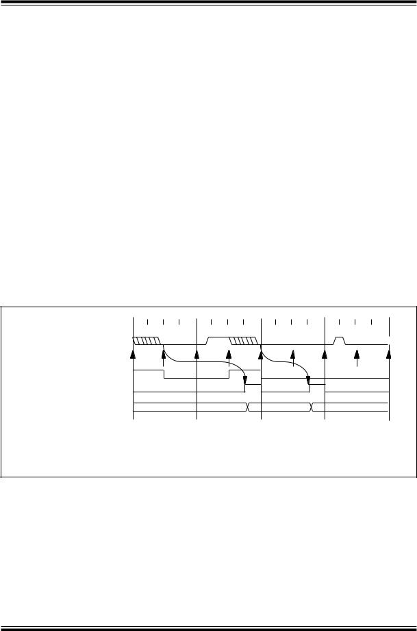
PIC12C5XX
6.1Using Timer0 with an External Clock
When an external clock input is used for Timer0, it must meet certain requirements. The external clock requirement is due to internal phase clock (TOSC) synchronization. Also, there is a delay in the actual incrementing of Timer0 after synchronization.
6.1.1EXTERNAL CLOCK SYNCHRONIZATION
When no prescaler is used, the external clock input is the same as the prescaler output. The synchronization of T0CKI with the internal phase clocks is accomplished by sampling the prescaler output on the Q2 and Q4 cycles of the internal phase clocks (Figure 6-4). Therefore, it is necessary for T0CKI to be high for at least 2TOSC (and a small RC delay of 20 ns) and low for at least 2TOSC (and a small RC delay of 20 ns). Refer to the electrical specification of the desired device.
When a prescaler is used, the external clock input is divided by the asynchronous ripple counter-type prescaler so that the prescaler output is symmetrical. For the external clock to meet the sampling requirement, the ripple counter must be taken into account. Therefore, it is necessary for T0CKI to have a period of at least 4TOSC (and a small RC delay of 40 ns) divided by the prescaler value. The only requirement on T0CKI high and low time is that they do not violate the minimum pulse width requirement of 10 ns. Refer to parameters 40, 41 and 42 in the electrical specification of the desired device.
6.1.2TIMER0 INCREMENT DELAY
Since the prescaler output is synchronized with the internal clocks, there is a small delay from the time the external clock edge occurs to the time the Timer0 module is actually incremented. Figure 6-4 shows the delay from the external clock edge to the timer incrementing.
6.1.3OPTION REGISTER EFFECT ON GP2 TRIS
If the option register is set to read TIMER0 from the pin, the port is forced to an input regardless of the TRIS register setting.
FIGURE 6-4: TIMER0 TIMING WITH EXTERNAL CLOCK
External Clock Input or Prescaler Output (2)
External Clock/Prescaler
Output After Sampling
Increment Timer0 (Q4)
Timer0
Q1 |
Q2 |
Q3 |
Q4 |
Q1 |
Q2 |
Q3 |
Q4 |
Q1 |
Q2 |
Q3 |
Q4 |
Q1 |
Q2 |
Q3 |
Q4 |
|
|
|
|
|
|
|
|
|
|
|
|
|
Small pulse |
||
|
|
|
|
|
|
|
|
|
|
|
|
|
misses sampling |
||
(3) |
|
(1) |
|
|
|
|
|
|
|
|
|
|
|
|
|
|
|
|
|
|
|
|
|
|
|
|
|
|
|
|
|
|
|
|
|
T0 |
|
|
|
T0 + 1 |
|
|
|
T0 + 2 |
|
||
Note 1: Delay from clock input change to Timer0 increment is 3Tosc to 7Tosc. (Duration of Q = Tosc). Therefore, the error in measuring the interval between two edges on Timer0 input = ± 4Tosc max.
2:External clock if no prescaler selected, Prescaler output otherwise.
3:The arrows indicate the points in time where sampling occurs.
1998 Microchip Technology Inc. |
DS40139D-page 25 |
PIC12C5XX
6.2Prescaler
An 8-bit counter is available as a prescaler for the Timer0 module, or as a postscaler for the Watchdog Timer (WDT), respectively (Section 7.6). For simplicity, this counter is being referred to as “prescaler” throughout this data sheet. Note that the prescaler may be used by either the Timer0 module or the WDT, but not both. Thus, a prescaler assignment for the Timer0 module means that there is no prescaler for the WDT, and vice-versa.
The PSA and PS2:PS0 bits (OPTION<3:0>) determine prescaler assignment and prescale ratio.
When assigned to the Timer0 module, all instructions writing to the TMR0 register (e.g., CLRF 1, MOVWF 1, BSF 1,x, etc.) will clear the prescaler. When assigned to WDT, a CLRWDT instruction will clear the prescaler along with the WDT. The prescaler is neither readable nor writable. On a RESET, the prescaler contains all '0's.
6.2.1SWITCHING PRESCALER ASSIGNMENT
The prescaler assignment is fully under software control (i.e., it can be changed “on the y”fl during program execution). To avoid an unintended device RESET, the following instruction sequence (Example 6-1) must be executed when changing the prescaler assignment from Timer0 to the WDT.
EXAMPLE 6-1: CHANGING PRESCALER (TIMER0→WDT)
1.CLRWDT |
|
;Clear WDT |
2.CLRF |
TMR0 |
;Clear TMR0 & Prescaler |
3.MOVLW |
'00xx1111’b |
;These 3 lines (5, 6, 7) |
4.OPTION |
|
; are required only if |
|
|
; desired |
5.CLRWDT |
|
;PS<2:0> are 000 or 001 |
6.MOVLW |
'00xx1xxx’b |
;Set Postscaler to |
7.OPTION |
|
; desired WDT rate |
To change prescaler from the WDT to the Timer0 module, use the sequence shown in Example 6-2. This sequence must be used even if the WDT is disabled. A CLRWDT instruction should be executed before switching the prescaler.
EXAMPLE 6-2: CHANGING PRESCALER (WDT→TIMER0)
CLRWDT |
;Clear WDT and |
|
;prescaler |
MOVLW 'xxxx0xxx' |
;Select TMR0, new |
|
;prescale value and |
|
;clock source |
OPTION |
|
FIGURE 6-5: BLOCK DIAGRAM OF THE TIMER0/WDT PRESCALER
TCY ( = Fosc/4) |
|
|
|
|
|
|
|
|
|
|
|
|
|
|
|
|
|
|
|
|
|
|
|
|
|
|
|
|
Data Bus |
||||||||
|
|
|
|
|
|
|
|
|
|
|
|
|
|
|
|
|
|
|
|
|
|
|
|
|
|
|
|
||||||||||
|
|
|
|
|
|
|
|
|
|
|
|
|
|
|
|
|
|
|
|
|
|
|
|
|
|
|
|
|
|
|
|
|
|
|
|
||
GP2/T0CKI |
|
0 |
|
|
|
|
|
|
|
|
|
|
|
|
|
|
|
|
|
|
|
|
|
|
8 |
||||||||||||
|
|
M |
1 |
|
|
|
|
|
|
|
|
|
|
||||||||||||||||||||||||
|
|
|
|
|
|
|
|
|
|
|
|
|
|
|
|
|
|
|
|||||||||||||||||||
|
Pin |
|
|
|
|
|
U |
|
M |
|
|
|
|
|
|
|
|
|
|
|
|
||||||||||||||||
|
|
|
|
|
|
|
|
|
|
|
|
|
|
|
|
|
|
|
|||||||||||||||||||
|
|
|
|
|
|
|
|
|
|
|
|
|
|
|
|
|
|
|
|
|
|
|
|||||||||||||||
|
|
|
|
|
|
|
|
|
|
|
1 |
|
X |
|
|
|
|
U |
|
|
|
|
|
Sync |
|
|
|
TMR0 reg |
|||||||||
|
|
|
|
|
|
|
|
|
|
|
|
|
|
|
|
|
|
|
|
|
|
|
|
|
|
|
|
|
2 |
|
|
|
|||||
|
|
|
|
|
|
|
|
|
|
|
|
|
|
|
|
|
|
|
|
|
|
|
|
|
|
|
|
|
|
|
|
||||||
|
|
|
|
|
|
|
|
|
|
|
|
|
|
|
|
|
|
|
|
|
|
|
|
|
|
|
|
|
|
|
|
||||||
|
|
|
|
|
|
|
|
|
|
|
|
|
|
|
|
|
|
|
|
||||||||||||||||||
|
|
|
|
|
|
|
|
|
|
|
|
|
|
|
|
|
|
|
|
|
|
0 |
X |
|
|
|
|
|
Cycles |
|
|
|
|
|
|||
|
|
|
|
|
|
|
|
|
|
|
|
|
|
|
|
|
|
|
|
|
|
|
|
|
|
|
|
|
|
|
|
|
|
|
|
||
|
|
|
|
|
|
|
|
|
|
|
|
|
|
|
|
|
|
|
|
|
|
|
|
|
|
|
|
|
|
|
|
|
|
|
|
|
|
|
|
|
|
|
|
|
|
|
|
|
|
|
|
|
|
|
|
|
|
|
|
|
|
|
|
|
|
|
|
|
|
|
|
|
|
|
|
|
|
|
|
|
|
|
|
|
|
|
|
|
|
|
|
|
|
|
|
|
|
|
|
|
|
|
|
|
|
|
|
|
|
|
|
|
|
|
|
T0SE |
|
|
|
|
|
|
|
|
|
|
|
|
|
|
|
|
|
|
|
|
|
|
|
|
|
|
|
||||||||
|
|
|
|
T0CS |
|
|
|
|
|
|
|
|
|
|
|
|
|
|
|
|
|
|
|||||||||||||||
|
|
|
|
|
|
|
|
|
|
|
|
|
|
|
|
|
|
|
PSA |
|
|
|
|
|
|
|
|
|
|
|
|
||||||
|
|
|
|
|
|
|
|
|
|
|
|
|
|
|
|
|
|
|
|
|
|
|
|
|
|
|
|
|
|
|
|
|
|
|
|
||
|
|
|
|
|
|
|
|
|
|
|
|
|
|
|
|
|
|
|
|
|
|
|
|
|
|
|
|
|
|
|
|
|
|
|
|
|
|
|
|
|
|
|
|
|
|
|
0 |
|
|
|
|
|
|
|
|
|
|
|
|
|
|
|
|
|
|
|
|
|
|
|
|
|
|
|
|
|
|
|
|
|
|
|
|
|
|
M |
|
|
|
|
|
|
8-bit Prescaler |
|
|
|
|
|
|
|
|
|
|
|
|
||||||||
|
|
|
|
|
|
|
|
|
|
|
|
|
|
|
|
|
|
|
|
|
|
|
|
|
|
|
|
|
|
||||||||
|
|
|
|
|
|
|
|
|
|
|
|
|
|
|
|
|
|
|
|
|
|
|
|
|
|
|
|
|
|
|
|
|
|
|
|
||
|
|
|
|
|
|
|
|
|
|
|
|
U |
|
|
|
|
|
|
|
|
|
|
|
|
|
|
|
|
|
|
|
|
|
|
|
|
|
Watchdog |
|
1 |
|
X |
|
|
|
|
|
|
8 |
|
|
|
|
|
|
|
|
|
|
|
|
|
|
|
|
||||||||||
|
|
|
|
|
|
|
|
|
|
|
|
|
|
|
|
|
|
|
|
|
|
|
|
|
|
||||||||||||
|
|
|
|
|
|
|
|
|
|
|
|
|
|
|
|
|
|
|
|
|
|
|
|
|
|
|
|
|
|
|
|
|
|||||
Timer |
|
|
|
|
|
|
|
|
|
|
|
|
|
|
|
|
|
|
|
|
|
|
|
|
|
|
|
|
|
|
|
|
|
|
|||
|
|
|
|
|
|
|
|
|
|
|
|
|
|
|
|
|
|
|
|
|
|
|
|
|
|
|
|||||||||||
|
|
|
|
|
|
|
|
|
|
|
|
|
|
|
|
|
|
|
|
8 - to - 1MUX |
|
|
|
|
PS2:PS0 |
|
|
|
|
|
|||||||
|
|
|
|
|
|
|
|
|
|
|
|
|
|
|
|
|
|
|
|
|
|
|
|
|
|||||||||||||
|
|
|
|
|
|
|
|
|
|
|
|
|
|
|
|
|
|
|
|
|
|
|
|
|
|
|
|
||||||||||
|
|
|
|
|
|
|
|
|
|
|
|
|
|
|
|
|
|
|
|
|
|
|
|
|
|
|
|
|
|
|
|
|
|
|
|
|
|
|
|
|
|
|
|
|
|
|
|
|
|
PSA |
|
|
|
|
|
|
|
|
|
|
|
|
|
|
|
|
|
|
|
|
|
|
|
||
|
|
|
|
|
|
|
|
|
|
|
|
|
|
|
|
|
|
|
|
|
|
|
|
|
|
|
|
|
|
|
|
|
|
|
|
|
|
|
|
|
|
|
|
|
|
|
|
|
|
|
|
|
|
|
|
|
|
|
|
|
|
|
|
|
|
|
|
|
|
|
|
|
|
|
|
0 1
WDT Enable bit
MUX |
PSA |
WDT
Time-Out
Note: T0CS, T0SE, PSA, PS2:PS0 are bits in the OPTION register.
DS40139D-page 26 |
1998 Microchip Technology Inc. |

PIC12C5XX
7.0SPECIAL FEATURES OF THE CPU
What sets a microcontroller apart from other processors are special circuits to deal with the needs of real-time applications. The PIC12C5XX family of microcontrollers has a host of such features intended to maximize system reliability, minimize cost through elimination of external components, provide power saving operating modes and offer code protection. These features are:
•Oscillator selection
•Reset
-Power-On Reset (POR)
-Device Reset Timer (DRT)
-Wake-up from SLEEP on pin change
•Watchdog Timer (WDT)
•SLEEP
•Code protection
•ID locations
•In-circuit Serial Programming
The PIC12C5XX has a Watchdog Timer which can be shut off only through configuration bit WDTE. It runs off of its own RC oscillator for added reliability. If using XT or LP selectable oscillator options, there is always an 18 ms (nominal) delay provided by the Device Reset Timer (DRT), intended to keep the chip in reset until the crystal oscillator is stable. If using INTRC or EXTRC there is an 18 ms delay only on VDD power-up. With this timer on-chip, most applications need no external reset circuitry.
The SLEEP mode is designed to offer a very low current power-down mode. The user can wake-up from SLEEP through a change on input pins or through a Watchdog Timer time-out. Several oscillator options are also made available to allow the part to fit the application, including an internal 4 MHz oscillator. The EXTRC oscillator option saves system cost while the LP crystal option saves power. A set of configuration bits are used to select various options.
7.1Configuration Bits
The PIC12C5XX configuration word consists of 12 bits. Configuration bits can be programmed to select various device configurations. Two bits are for the selection of the oscillator type, one bit is the Watchdog Timer enable bit, and one bit is the MCLR enable bit.
FIGURE 7-1: |
CONFIGURATION WORD FOR PIC12C5XX |
|
|
|
|
|
|
|
|
||||||||||||||||||
|
|
|
|
|
|
|
|
|
|
|
|
|
|
|
|
|
|
|
|
|
|
|
|
|
|
||
|
|
|
|
|
|
|
|
|
|
|
|
|
|
|
|
|
|
|
|
|
|
|
|
|
|
|
|
|
— |
|
|
— |
— |
|
|
— |
|
— |
|
— |
— |
MCLRE |
CP |
WDTE |
FOSC1 |
FOSC0 |
|
Register: |
CONFIG |
|
|||||
|
bit11 |
10 |
|
9 |
|
|
8 |
|
7 |
|
6 |
5 |
4 |
3 |
2 |
1 |
|
bit0 |
|
Address(1): |
FFFh |
|
|||||
|
bit 11-5: |
Unimplemented |
|
|
|
|
|
|
|
|
|
|
|
|
|
|
|
|
|||||||||
|
bit 4: |
MCLRE: |
|
|
enable bit. |
|
|
|
|
|
|
|
|
|
|
|
|
||||||||||
|
MCLR |
|
|
|
|
|
|
|
|
|
|
|
|
||||||||||||||
|
|
|
|
1 |
= |
MCLR |
pin enabled |
|
|
|
|
|
|
|
|
|
|
|
|
|
|
||||||
|
|
|
|
0 |
= |
MCLR |
tied to VDD, (Internally) |
|
|
|
|
|
|
|
|
|
|
|
|
||||||||
|
bit 3: |
CP: Code protection bit. |
|
|
|
|
|
|
|
|
|
|
|
|
|
|
|||||||||||
|
|
|
|
1 |
= Code protection off |
|
|
|
|
|
|
|
|
|
|
|
|
|
|
||||||||
|
|
|
|
0 |
= Code protection on |
|
|
|
|
|
|
|
|
|
|
|
|
|
|
||||||||
|
bit |
2: |
|
WDTE: Watchdog timer enable bit |
|
|
|
|
|
|
|
|
|
|
|
|
|||||||||||
|
|
|
|
1 |
= WDT enabled |
|
|
|
|
|
|
|
|
|
|
|
|
|
|
|
|
||||||
|
|
|
|
0 |
= WDT disabled |
|
|
|
|
|
|
|
|
|
|
|
|
|
|
||||||||
|
bit |
1-0: |
|
FOSC1:FOSC0: Oscillator selection bits |
|
|
|
|
|
|
|
|
|
|
|
||||||||||||
|
|
|
|
11 = EXTRC - external RC oscillator |
|
|
|
|
|
|
|
|
|
|
|
||||||||||||
|
|
|
|
10 = INTRC - internal RC oscillator |
|
|
|
|
|
|
|
|
|
|
|
||||||||||||
|
|
|
|
01 = XT oscillator |
|
|
|
|
|
|
|
|
|
|
|
|
|
|
|
|
|||||||
|
|
|
|
00 = LP oscillator |
|
|
|
|
|
|
|
|
|
|
|
|
|
|
|
|
|||||||
|
Note 1: |
Refer to the PIC12C5XX Programming Specifications to determine how to access the |
|
|
|
|
|
||||||||||||||||||||
|
|
|
|
configuration word. This register is not user addressable during device operation. |
|
|
|
|
|
||||||||||||||||||
|
|
|
|
|
|
|
|
|
|
|
|
|
|
|
|
|
|
|
|
|
|
|
|
|
|
|
|
1998 Microchip Technology Inc. |
DS40139D-page 27 |
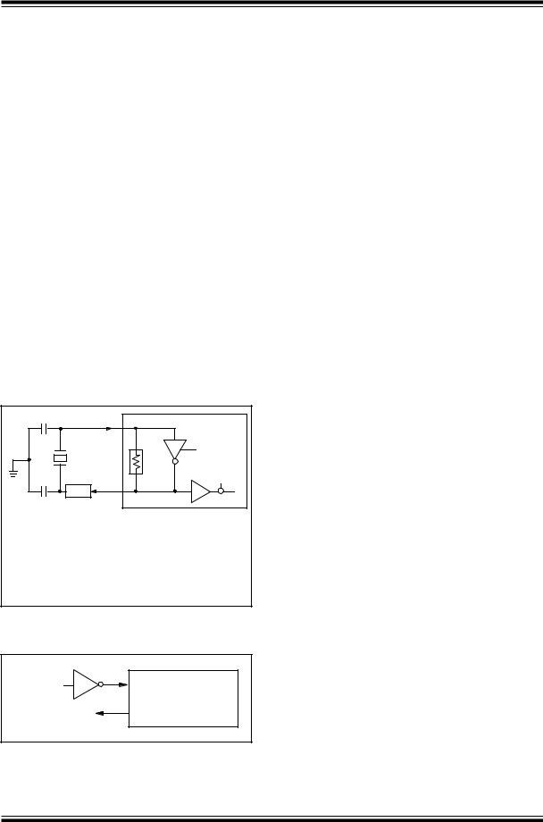
PIC12C5XX
7.2Oscillator Configurations
7.2.1OSCILLATOR TYPES
The PIC12C5XX can be operated in four different oscillator modes. The user can program two configuration bits (FOSC1:FOSC0) to select one of these four modes:
• LP: |
Low Power Crystal |
• XT: Crystal/Resonator
•INTRC: Internal 4 MHz Oscillator
•EXTRC: External Resistor/Capacitor
7.2.2CRYSTAL OSCILLATOR / CERAMIC RESONATORS
In XT or LP modes, a crystal or ceramic resonator is connected to the GP5/OSC1/CLKIN and GP4/OSC2 pins to establish oscillation (Figure 7-2). The PIC12C5XX oscillator design requires the use of a parallel cut crystal. Use of a series cut crystal may give a frequency out of the crystal manufacturers specifications. When in XT or LP modes, the device can have an external clock source drive the GP5/ OSC1/CLKIN pin (Figure 7-3).
FIGURE 7-2: CRYSTAL OPERATION (OR CERAMIC RESONATOR) (XT OR LP OSC CONFIGURATION)
C1(1) |
PIC12C5XX |
OSC1 |
|
XTAL |
SLEEP |
RF(3) |
|
|
To internal |
RS(2) OSC2 |
logic |
|
|
C2(1) |
|
Note 1: See Capacitor Selection tables for recommended values of C1 and C2.
2:A series resistor (RS) may be required for AT strip cut crystals.
3:RF approximate value = 10 MΩ.
FIGURE 7-3: EXTERNAL CLOCK INPUT OPERATION (XT OR LP OSC CONFIGURATION)
Clock from |
OSC1 |
ext. system |
PIC12C5XX |
Open |
OSC2 |
TABLE 7-1: CAPACITOR SELECTION FOR CERAMIC RESONATORS - PIC12C5XX
Osc |
Resonator |
Cap. Range |
Cap. Range |
Type |
Freq |
C1 |
C2 |
|
|
|
|
|
|
|
|
XT |
4.0 MHz |
30 pF |
30 pF |
These values are for design guidance only. Since each resonator has its own characteristics, the user should consult the resonator manufacturer for appropriate values of external components.
TABLE 7-2: CAPACITOR SELECTION FOR CRYSTAL OSCILLATOR - PIC12C5XX
Osc |
Resonator |
Cap.Range |
Cap. Range |
Type |
Freq |
C1 |
C2 |
|
|
|
|
|
|
|
|
LP |
32 kHz(1) |
15 pF |
15 pF |
XT |
200 kHz |
47-68 pF |
47-68 pF |
|
1 MHz |
15 pF |
15 pF |
|
4 MHz |
15 pF |
15 pF |
Note 1: For VDD > 4.5V, C1 = C2 ≈ 30 pF is recommended.
These values are for design guidance only. Rs may be required to avoid overdriving crystals with low drive level specification. Since each crystal has its own characteristics, the user should consult the crystal manufacturer for appropriate values of external components.
DS40139D-page 28 |
1998 Microchip Technology Inc. |

PIC12C5XX
7.2.3EXTERNAL CRYSTAL OSCILLATOR CIRCUIT
Either a prepackaged oscillator or a simple oscillator circuit with TTL gates can be used as an external crystal oscillator circuit. Prepackaged oscillators provide a wide operating range and better stability. A well-designed crystal oscillator will provide good performance with TTL gates. Two types of crystal oscillator circuits can be used: one with parallel resonance, or one with series resonance.
Figure 7-4 shows implementation of a parallel resonant oscillator circuit. The circuit is designed to use the fundamental frequency of the crystal. The 74AS04 inverter performs the 180-degree phase shift that a parallel oscillator requires. The 4.7 kΩ resistor provides the negative feedback for stability. The 10 kΩ potentiometers bias the 74AS04 in the linear region. This circuit could be used for external oscillator designs.
FIGURE 7-4: EXTERNAL PARALLEL RESONANT CRYSTAL OSCILLATOR CIRCUIT
+5V |
|
To Other |
|
|
|
10k |
|
Devices |
|
|
|
4.7k |
74AS04 |
PIC12C5XX |
74AS04 |
CLKIN |
|
|
10k |
|
XTAL |
|
|
10k |
|
|
20 pF |
20 pF |
|
Figure 7-5 shows a series resonant oscillator circuit. This circuit is also designed to use the fundamental frequency of the crystal. The inverter performs a 180degree phase shift in a series resonant oscillator circuit. The 330 Ω resistors provide the negative feedback to bias the inverters in their linear region.
FIGURE 7-5: EXTERNAL SERIES RESONANT CRYSTAL OSCILLATOR CIRCUIT
|
|
To Other |
|
330 |
330 |
Devices |
|
PIC12C5XX |
|||
|
|
||
74AS04 |
74AS04 |
74AS04 |
|
|
|
CLKIN |
|
|
0.1 F |
|
|
|
XTAL |
|
7.2.4EXTERNAL RC OSCILLATOR
For timing insensitive applications, the RC device option offers additional cost savings. The RC oscillator frequency is a function of the supply voltage, the resistor (Rext) and capacitor (Cext) values, and the operating temperature. In addition to this, the oscillator frequency will vary from unit to unit due to normal process parameter variation. Furthermore, the difference in lead frame capacitance between package types will also affect the oscillation frequency, especially for low Cext values. The user also needs to take into account variation due to tolerance of external R and C components used.
Figure 7-6 shows how the R/C combination is connected to the PIC12C5XX. For Rext values below 2.2 kΩ, the oscillator operation may become unstable, or stop completely. For very high Rext values (e.g., 1 MΩ) the oscillator becomes sensitive to noise, humidity and leakage. Thus, we recommend keeping Rext between 3 kΩ and 100 kΩ.
Although the oscillator will operate with no external capacitor (Cext = 0 pF), we recommend using values above 20 pF for noise and stability reasons. With no or small external capacitance, the oscillation frequency can vary dramatically due to changes in external capacitances, such as PCB trace capacitance or package lead frame capacitance.
The Electrical Specifications sections show RC frequency variation from part to part due to normal process variation. The variation is larger for larger R (since leakage current variation will affect RC frequency more for large R) and for smaller C (since variation of input capacitance will affect RC frequency more).
Also, see the Electrical Specifications sections for variation of oscillator frequency due to VDD for given Rext/Cext values as well as frequency variation due to operating temperature for given R, C, and VDD values.
FIGURE 7-6: EXTERNAL RC OSCILLATOR MODE
VDD |
|
Rext |
Internal |
|
|
OSC1 |
clock |
N |
|
Cext |
PIC12C5XX |
|
|
VSS |
|
1998 Microchip Technology Inc. |
DS40139D-page 29 |
PIC12C5XX
7.2.5INTERNAL 4 MHz RC OSCILLATOR
The internal RC oscillator provides a fixed 4 MHz (nominal) system clock at VDD = 5V and 25°C, see “Electrical Specifications” section for information on variation over voltage and temperature..
In addition, a calibration instruction is programmed into the top of memory which contains the calibration value for the internal RC oscillator. This location is never code protected regardless of the code protect settings. This value is programmed as a MOVLW XX instruction where XX is the calibration value, and is placed at the reset vector. This will load the W register with the calibration value upon reset and the PC will then roll over to the users program at address 0x000.The user then has the option of writing the value to the OSCCAL Register (05h) or ignoring it.
OSCCAL, when written to with the calibration value, will “trim” the internal oscillator to remove process variation from the oscillator frequency. .
Note: Please note that erasing the device will also erase the pre-programmed internal calibration value for the internal oscillator. The calibration value must be read prior to erasing the part. so it can be reprogrammed correctly later.
For the PIC12C508A and PIC12C509A, bits <7:2>, CAL5-CAL0 are used for calibration. Adjusting CAL5- 0 from 000000 to 111111 yields a higher clock speed. Note that bits 1 and 0 of OSCCAL are unimplemented and should be written as 0 when modifying OSCCAL for compatibility with future devices.
For the PIC12C508 and PIC12C509, the lower 4 bits of the register are used. Writing a larger value in this location yields a higher clock speed.
7.3RESET
The device differentiates between various kinds of reset:
a)Power on reset (POR)
b)MCLR reset during normal operation
c)MCLR reset during SLEEP
d)WDT time-out reset during normal operation
e)WDT time-out reset during SLEEP
f)Wake-up from SLEEP on pin change
Some registers are not reset in any way; they are unknown on POR and unchanged in any other reset. Most other registers are reset to “reset state”on poweron reset (POR), MCLR, WDT or wake-up on pin change reset during normal operation. They are not affected by a WDT reset during SLEEP or MCLR reset during SLEEP, since these resets are viewed as resumption of normal operation. The exceptions to this
are TO, PD, and GPWUF bits. They are set or cleared differently in different reset situations. These bits are used in software to determine the nature of reset. See Table 7-3 for a full description of reset states of all registers.
DS40139D-page 30 |
1998 Microchip Technology Inc. |
 Loading...