


MXIC MX28F1000PRI-12, MX28F1000PRI-70, MX28F1000PRI-90, MX28F1000PTC-12C4, MX28F1000PTC-70C4 Datasheet
...MX28F1000P
FEATURES
•131,072 bytes by 8-bit organization
•Fast access time: 70ns(Vcc:5V±5%; CL:35pF)
90/120ns(Vcc:5V±10%; CL:100pF)
•Low power consumption
–50mA maximum active current
–100uA maximum standby current
•Programming and erasing voltage 12V ± 5%
•Command register architecture
–Byte Programming (15us typical)
–Auto chip erase 5 seconds typical (including preprogramming time)
–Block Erase
•Optimized high density blocked architecture
–Four 4-KB blocks
1M-BIT [128K x 8] CMOS FLASH MEMORY
–Seven 16-KB blocks
•Auto Erase (chip & block) and Auto Program
–DATA polling
–Toggle bit
•10,000 minimum erase/program cycles
•Latch-up protected to 100mA from -1 to VCC+1V
•Advanced CMOS Flash memory technology
•Compatible with JEDEC-standard byte-wide 32-pin EPROM pinouts
•Package type:
–32-pin plastic DIP
–32-pin PLCC
–32-pin TSOP (Type 1)
GENERAL DESCRIPTION
The MX28F1000P is a 1-mega bit Flash memory organized as 128K bytes of 8 bits each. MXIC's Flash memories offer the most cost-effective and reliable read/write non-volatile random access memory. The MX28F1000P is packaged in 32-pin PDIP, PLCC and TSOP. It is designed to be reprogrammed and erased in-system or in-standard EPROM programmers.
The standard MX28F1000P offers access times as fast as 70 ns, allowing operation of high-speed microprocessors without wait states. To eliminate bus contention, the MX28F1000P has separate chip enable (CE) and output enable (OE ) controls.
MXIC's Flash memories augment EPROM functionality with in-circuit electrical erasure and programming. The MX28F1000P uses a command register to manage this functionality, while maintaining a standard 32-pin pinout. The command register allows for 100% TTL level control inputs and fixed power supply levels during erase and programming, while maintaining maximum EPROM compatibility.
MXIC Flash technology reliably stores memory contents even after 10,000 erase and program cycles. The MXIC cell is designed to optimize the erase and programming mechanisms. In addition, the combination of advanced tunnel oxide processing and low internal electric fields for erase and programming operations produces reliable cycling. The
MX28F1000P uses a 12.0V ± 5% VPP supply to perform the Auto Program/Erase algorithms.
The highest degree of latch-up protection is achieved with MXIC's proprietary non-epi process. Latch-up protection is proved for stresses up to 100 milliamps on address and data pin from -1V to VCC + 1V.
P/N: PM0340 |
1 |
REV. 1.6,JAN. 19, 1999 |
|
MX28F1000P
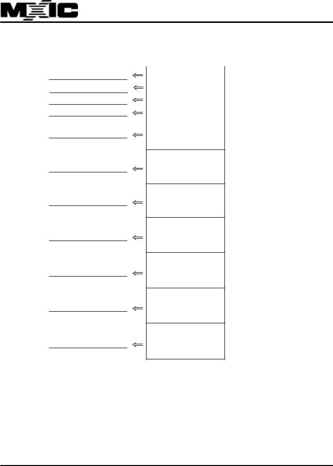
MX28F1000P Block Address and Block Structure
A16 |
A15 |
A14 |
A13 |
A12 |
|
|
|
|
|
|
|
1 |
1 |
1 |
1 |
1 |
4k |
1 |
1 |
1 |
1 |
0 |
4k |
1 |
1 |
1 |
0 |
1 |
4k |
1 |
1 |
1 |
0 |
0 |
4k |
1 |
1 |
0 |
X |
X |
16k |
1 0 1 X X |
16k |
1 0 0 X X |
16k |
0 1 1 X X |
16k |
0 1 0 X X |
16k |
0 0 1 X X |
16k |
0 0 0 X X |
16k |
|
A [ 1 6 : 0 ] 1 F F F F 1 F 0 0 0
1 E F F F
1 E 0 0 0
1 D F F F
1 D 0 0 0
1 C F F F
1 C 0 0 0
1 B F F F
1 8 0 0 0
1 7 F F F
1 4 0 0 0
1 3 F F F
1 0 0 0 0
0 F F F F
0 C 0 0 0
0 B F F F
0 8 0 0 0
0 7 F F F
0 4 0 0 0
0 3 F F F
0 0 0 0 0
P/N: PM0340 |
REV. 1.6, JAN. 19, 1999 |
2
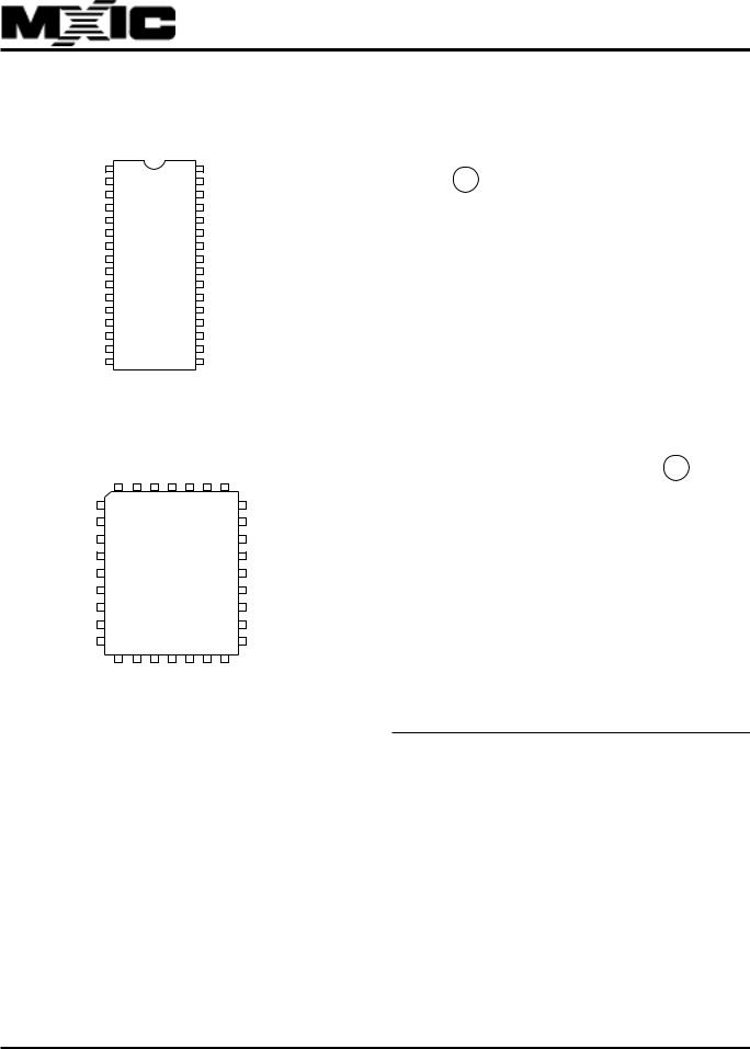
PIN CONFIGURATIONS
32 PDIP
VPP |
1 |
|
32 |
VCC |
|||
A16 |
2 |
|
31 |
WE |
|||
A15 |
3 |
|
30 |
NC |
|||
A12 |
4 |
|
29 |
A14 |
|||
A7 |
5 |
MX28F1000P |
28 |
A13 |
|||
A6 |
6 |
27 |
A8 |
||||
|
|||||||
A5 |
7 |
|
26 |
A9 |
|||
A4 |
8 |
|
25 |
A11 |
|||
A3 |
9 |
|
24 |
OE |
|
||
A2 |
10 |
|
23 |
A10 |
|||
A1 |
11 |
|
22 |
CE |
|
||
A0 |
12 |
|
21 |
Q7 |
|||
Q0 |
13 |
|
20 |
Q6 |
|||
Q1 |
14 |
|
19 |
Q5 |
|||
Q2 |
15 |
|
18 |
Q4 |
|||
GND |
16 |
|
17 |
Q3 |
|||
32 PLCC
|
A12 |
A15 |
A16 |
VPP |
VCC |
|
WE |
NC |
|
|
|
|
|
|
|
|
|||||||
|
|
|
|
|
|||||||
|
4 |
|
|
1 |
32 |
|
|
30 |
|
|
|
A7 |
5 |
|
|
|
|
|
|
29 |
A14 |
||
A6 |
|
|
|
|
|
|
|
|
A13 |
||
A5 |
|
|
|
|
|
|
|
|
A8 |
||
A4 |
|
|
|
|
|
|
|
|
A9 |
||
A3 |
9 |
MX28F1000P |
25 |
A11 |
|||||||
|
|
|
|
|
|
|
|
|
|
|
|
A2 |
|
|
|
|
|
|
|
|
OE |
||
A1 |
|
|
|
|
|
|
|
|
A10 |
||
|
|
|
|
|
|
|
|
|
|
|
|
A0 |
|
|
|
|
|
|
|
|
CE |
||
Q0 |
13 |
|
|
17 |
|
|
|
21 |
Q7 |
||
|
14 |
|
|
|
|
|
20 |
|
|
|
|
|
Q1 |
Q2 |
VSS |
Q3 |
Q4 |
|
Q5 |
Q6 |
|
|
|
P/N: PM0340
MX28F1000P
TSOP (TYPE 1)
|
|
|
|
|
|
32 |
|
|
|
|
|
A11 |
|
1 |
|
|
OE |
||||||
|
A9 |
|
2 |
|
31 |
|
A10 |
||||
|
|
|
|
|
|
30 |
|
|
|
|
|
|
A8 |
|
3 |
|
|
CE |
|||||
A13 |
|
4 |
|
29 |
|
Q7 |
|||||
A14 |
|
5 |
|
28 |
|
Q6 |
|||||
NC |
|
6 |
|
27 |
|
Q5 |
|||||
|
|
|
|
7 |
|
26 |
|
Q4 |
|||
WE |
|
MX28F1000P |
|
||||||||
VCC |
|
8 |
25 |
|
Q3 |
||||||
VPP |
|
9 |
|
24 |
|
GND |
|||||
A16 |
|
10 |
|
23 |
|
Q2 |
|||||
A15 |
|
11 |
|
22 |
|
Q1 |
|||||
A12 |
|
12 |
|
21 |
|
Q0 |
|||||
|
|
|
|||||||||
|
A7 |
|
13 |
|
20 |
|
A0 |
||||
|
|
|
|||||||||
|
A6 |
|
14 |
|
19 |
|
A1 |
||||
|
|
|
|||||||||
|
A5 |
|
15 |
|
18 |
|
A2 |
||||
|
|
|
|||||||||
|
A4 |
|
16 |
|
17 |
|
A3 |
||||
|
|
|
|||||||||
|
|
|
|
|
|
|
|
|
|
|
|
(NORMAL TYPE)
|
|
|
|
|
|
32 |
|
1 |
|
A11 |
|||
|
OE |
|
|
|
|||||||||
A10 |
|
31 |
|
2 |
|
A9 |
|||||||
|
|
|
|
|
|
30 |
|
3 |
|
A8 |
|||
|
|
CE |
|
|
|
||||||||
|
|
Q7 |
|
29 |
|
4 |
|
A13 |
|||||
|
|
Q6 |
|
28 |
|
5 |
|
A14 |
|||||
|
|
Q5 |
|
27 |
|
6 |
|
NC |
|||||
|
|
|
|
|
|
|
|
7 |
|
|
|
|
|
|
|
Q4 |
|
26 |
MX28F1000P |
|
WE |
||||||
|
|
Q3 |
|
25 |
8 |
|
VCC |
||||||
|
|
||||||||||||
GND |
|
24 |
|
9 |
|
VPP |
|||||||
|
|
Q2 |
|
23 |
|
10 |
|
A16 |
|||||
|
|
Q1 |
|
22 |
|
11 |
|
A15 |
|||||
|
|
Q0 |
|
21 |
|
12 |
|
A12 |
|||||
|
|
|
|||||||||||
|
|
A0 |
|
20 |
|
13 |
|
A7 |
|||||
|
|
|
|||||||||||
|
|
A1 |
|
19 |
|
14 |
|
A6 |
|||||
|
|
|
|||||||||||
|
|
A2 |
|
18 |
|
15 |
|
A5 |
|||||
|
|
|
|||||||||||
|
|
|
|
|
|
|
|
16 |
|
|
|
|
|
|
|
A3 |
|
17 |
|
|
A4 |
||||||
|
|
|
|||||||||||
|
|
|
|
|
|
|
|
|
|
|
|
|
|
(REVERSE TYPE)
PIN DESCRIPTION:
SYMBOL |
PIN NAME |
|||
A0~A16 |
Address Input |
|||
Q0~Q7 |
Data Input/Output |
|||
|
|
|
|
|
CE |
Chip Enable Input |
|||
|
|
|
|
|
|
|
|
|
|
OE |
Output Enable Input |
|||
|
|
|
|
|
|
|
|
|
|
WE |
Write enable Pin |
|||
|
|
|
|
|
VPP |
Program Supply Voltage |
|||
|
|
|
|
|
VCC |
Power Supply Pin (+5V) |
|||
|
|
|||
GND |
Ground Pin |
|||
|
|
|
|
|
REV. 1.6, JAN. 19, 1999
3

MX28F1000P
BLOCK DIAGRAM
CE |
CONTROL |
OE |
INPUT |
WE |
LOGIC |
ADDRESS
LATCH
A0-A16
AND
BUFFER
Q0-Q7
PROGRAM/ERASE |
MODE |
|
|
HIGH VOLTAGE |
LOGIC |
|
X- |
|
|
|
STATE |
|
|
HV |
COMMAND |
|
DECODER-Y |
MX28F1000P |
|||
|
|
REGISTER |
||
|
|
FLASH |
|
|
|
|
ARRAY |
ARRAY |
|
DECODER |
|
|
SOURCE |
|
|
|
|
DATA |
|
|
|
|
|
|
|
Y-PASS GATE |
|
DECODER |
|
|
|
|
|
|
SENSE |
PGM |
|
COMMAND |
|
DATA |
|
|||
|
|
|
||
AMPLIFIER HV |
|
DATA LATCH |
||
|
|
|
|
|
PROGRAM
DATA LATCH
I/O BUFFER
P/N: PM0340 |
REV. 1.6, JAN. 19, 1999 |
4

MX28F1000P
AUTOMATIC PROGRAMMING
The MX28F1000P is byte programmable using the Automatic Programming algorithm. The Automatic Programming algorithm does not require the system to time out or verify the data programmed. The typical room temperature chip programming time of the MX28F1000P is less than 5 seconds.
AUTOMATIC CHIP ERASE
The device may be erased using the Automatic Erase algorithm. The Automatic Erase algorithm automatically programs the entire array prior to electrical erase. The timing and verification of electrical erase are controlled internal to the device.
AUTOMATIC BLOCK ERASE
The MX28F1000P is block(s) erasable using MXIC's Auto Block Erase algorithm. Block erase modes allow blocks of the array to be erased in one erase cycle. The Automatic Block Erase algorithm automatically programs the specified block(s) prior to electrical erase. The timing and verification of electrical erase are controlled internal to the device.
AUTOMATIC PROGRAMMING ALGORITHM
MXIC's Automatic Programming algorithm requires the user to only write a program set-up command and a program command (program data and address). The device automatically times the programming pulse width, provides the program verify, and counts the number of sequences. A status bit similar to DATA polling and a status bit toggling between consecutive read cycles, provide feedback to the user as to the status of the programming operation.
AUTOMATIC ERASE ALGORITHM
MXIC's Automatic Erase algorithm requires the user to only write an erase set-up command and erase command. The device will automatically pre-program and verify the entire array. Then the device automatically times the erase pulse width, provides the erase verify, and counts the number of sequences. A status bit similar to DATA polling and a status bit toggling between consecutive read cycles, provide feedback to the user as to the status of the erase operation.
Commands are written to the command register using standard microprocessor write timings. Register contents serve as inputs to an internal state-machine which controls the erase and programming circuitry. During write cycles, the command register internally latches address and data needed for the programming and erase operations. For system design simplifica- tion, the MX28F1000P is designed to support either WE or CE controlled writes. During a system write cycle, addresses are latched on the falling edge of WE or CE whichever occurs last. Data is latched on the rising edge of WE or CE whichever occur first. To simplify the following discussion, the WE pin is used as the write cycle control pin throughout the rest of this text. All setup and hold times are with respect to the WE signal.
MXIC's Flash technology combines years of EPROM experience to produce the highest levels of quality, reliability, and cost effectiveness. The MX28F1000P electrically erases all bits simultaneously using Fowler-Nord- heim tunneling. The bytes are programmed one byte at a time using the EPROM programming mechanism of hot electron injection.
P/N: PM0340 |
REV. 1.6, JAN. 19, 1999 |
5

MX28F1000P
TABLE 1. COMMAND DEFINITIONS
COMMAND |
BUS |
|
FIRST BUS CYCLE |
|
SECOND BUS CYCLE |
|||
|
|
|||||||
|
|
|
|
|
|
|
|
|
|
CYCLES |
|
OPERATION |
ADDRESS |
DATA |
OPERATION |
ADDRESS |
DATA |
|
|
|
|
|
|
|
|
|
Read Memory |
1 |
|
Write |
X |
00H |
|
|
|
|
|
|
|
|
|
|
|
|
Read Identified codes |
2 |
|
Write |
X |
90H |
Read |
IA |
ID |
|
|
|
|
|
|
|
|
|
Setup auto erase/ |
2 |
|
Write |
X |
30H |
Write |
X |
30H |
auto erase (chip) |
|
|
|
|
|
|
|
|
|
|
|
|
|
|
|
|
|
Setup auto erase/ |
2 |
|
Write |
X |
20H |
Write |
EA |
D0H |
auto erase (block) |
|
|
|
|
|
|
|
|
|
|
|
|
|
|
|
|
|
Setup auto program/ |
2 |
|
Write |
X |
40H |
Write |
PA |
PD |
program |
|
|
|
|
|
|
|
|
|
|
|
|
|
|
|
|
|
Setup Erase/ |
2 |
|
Write |
X |
20H |
Write |
X |
20H |
Erase (chip) |
|
|
|
|
|
|
|
|
|
|
|
|
|
|
|
|
|
Setup Erase/ |
2 |
|
Write |
X |
60H |
Write |
EA |
60H |
Erase (block) |
|
|
|
|
|
|
|
|
|
|
|
|
|
|
|
|
|
Erase verify |
2 |
|
Write |
EVA |
A0H |
Read |
X |
EVD |
|
|
|
|
|
|
|
|
|
Reset |
2 |
|
Write |
X |
FFH |
Write |
X |
FFH |
|
|
|
|
|
|
|
|
|
Note: |
|
|
|
IA |
= |
Identifier address |
|
EA |
= Block of memory location to be erased |
|
|
PA |
= Address of memory location to be |
pro- |
|
|
|
grammed |
|
ID |
= |
Data read from location IA during device |
iden- |
|
|
tification |
|
PD |
= Data to be programmed at location PA |
|
|
EVA |
= |
Address of memory location to be read during |
|
|
|
erase verify. |
|
EVD = |
Data read from location EVA during erase |
||
|
|
verify. |
|
Auto modes have the build-in enchanced features.
Please use the auto erase mode whenever it is.
P/N: PM0340 |
REV. 1.6, JAN. 19, 1999 |
6

MX28F1000P
COMMAND DEFINITIONS
When low voltage is applied to the VPP pin, the contents of the command register default to 00H, enabling read-only operation.
Placing high voltage on the VPP pin enables read/write operations. Device operations are selected by writing specific data patterns into the command register. Table 1 defines these MX28F1000P register commands. Table 2 defines the bus operations of MX28F1000P.
TABLE 2. MX28F1000P BUS OPERATIONS
OPERATION |
|
VPP(1) |
A0 |
A9 |
CE |
OE |
WE |
DQ0-DQ7 |
|
|
|
|
|
|
|
|
|
READ-ONLY |
Read |
VPPL |
A0 |
A9 |
VIL |
VIL |
VIH |
Data Out |
|
|
|
|
|
|
|
|
|
|
Output Disable |
VPPL |
X |
X |
VIL |
VIH |
VIH |
Tri-State |
|
Standby |
VPPL |
X |
X |
VIH |
X |
X |
Tri-State |
|
Read Silicon ID (Mfr)(2) |
VPPL |
VIL |
VID(3) |
VIL |
VIL |
VIH |
Data = C2H |
|
|
|
|
|
|
|
|
|
|
Read Silicon ID (Device)(2) |
VPPL |
VIH |
VID(3) |
VIL |
VIL |
VIH |
Data = 1AH |
|
|
|
|
|
|
|
|
|
READ/WRITE |
Read |
VPPH |
A0 |
A9 |
VIL |
VIL |
VIH |
Data Out(4) |
|
Standby(5) |
VPPH |
X |
X |
VIH |
X |
X |
Tri-State |
|
Write |
VPPH |
A0 |
A9 |
VIL |
VIH |
VIL |
Data In(6) |
NOTES:
1.VPPL may be grounded, a no-connect with a resistor tied to ground, or < VCC + 2.0V. VPPH is the programming voltage specified for the device. When VPP = VPPL, memory contents can be read but not written or erased.
2.Manufacturer and device codes may also be accessed via a command register write sequence. Refer to Table 1. All other addresses are don't care.
3.VID is the Silicon-ID-Read high voltage.(11.5V to 13v)
4.Read operations with VPP = VPPH may access array data or Silicon ID codes.
5.With VPP at high voltage, the standby current equals ICC + IPP (standby).
6.Refer to Table 1 for valid Data-In during a write operation.
7.X can be VIL or VIH.
P/N: PM0340 |
REV. 1.6, JAN. 19, 1999 |
7

MX28F1000P
READ COMMAND
While VPP is high, for erase and programming, memory contents can also be accessed via the read command. The read operation is initiated by writing 00H into the command register. Microprocessor read cycles retrieve array data. The device remains enabled for reads until the command register contents are altered.
The default contents of the register upon VPP powerup is 00H. This default value ensures that no spurious alteration of memory contents occurs during the VPP power transition. Where the VPP supply is hard-wired to the MX28F1000P, the device powers up and remains enabled for reads until the command register contents are changed.
SILICON-ID-READ COMMAND
Flash-memories are intended for use in applications where the local CPU alters memory contents. As such, manufacturerand device-codes must be accessible while the device resides in the target system. PROM programmers typically access signature codes by raising A9 to a high voltage. However, multiplexing high voltage onto address lines is not a desired systemdesign practice.
The MX28F1000P contains a Silicon-ID-Read operation to supplement traditional PROMprogramming methodology. The operation is initiated by writing 90H into the command register. Following the command write, a read cycle from address 0000H retrieves the manufacturer code of C2H. A read cycle from address 0001H returns the device code of 1AH.
SET-UP AUTOMATIC CHIP ERASE/ERASE COMMANDS
The automatic chip erase does not require the device to be entirely pre-programmed prior to excuting the Automatic set-up erase command and Automatic chip erase command. Upon executing the Automatic chip erase command, the device automatically will program and verify the entire memory for an all-zero data pattern. When the device is automatically verified to contain an all-zero pattern, a self-timed chip erase and verify begin. The erase and verify operations are complete when the data on DQ7 is "1" at which time the
device returns to the Read mode. The system is not required to provide any control or timing during these operations.
When using the Automatic Chip Erase algorithm, note that the erase automatically terminates when adequate erase margin has been achieved for the memory array(no erase verify command is required). The margin voltages are internally generated in the same manner as when the standard erase verify command is used.
The Automatic set-up erase command is a commandonly operation that stages the device for automatic electrical erasure of all bytes in the array. Automatic set-up erase is performed by writing 30H to the command register.
To command automatic chip erase, the command 30H must be written again to the command register. The automatic chip erase begins on the rising edge of the WE and terminates when the data on DQ7 is "1" and the data on DQ6 stops toggling for two consecutive read cycles, at which time the device returns to the Read mode.
SET-UP AUTOMATIC BLOCK ERASE/ERASE COMMANDS
The automatic block erase does not require the device to be entirely pre-programmed prior to executing the Automatic set-up block erase command and Automatic block erase command. Upon executing the Automatic block erase command, the device automatically will program and verify the block(s) memory for an all-zero data pattern. The system is not required to provide any controls or timing during these operations.
When the block(s) is automatically verified to contain an all-zero pattern, a self-timed block erase and verify begin. The erase and verify operations are complete when the data on DQ7 is "1" and the data on DQ6 stops toggling for two consecutive read cycles, at which time the device returns to the Read mode. The system is not required to provide any control or timing during these operations.
When using the Automatic Block Erase algorithm, note that the erase automatically terminates when adequate erase margin has been achieved for the memory array (no erase verify command is required). The margin
P/N: PM0340 |
REV. 1.6, JAN. 19, 1999 |
8

MX28F1000P
voltages are internally generated in the same manner as when the standard erase verify command is used.
The Automatic set-up block erase command is a command only operation that stages the device for automatic electrical erasure of selected blocks in the array. Automatic set-up block erase is performed by writing 20H to the command register.
To enter automatic block erase, the user must write the command D0H to the command register. Block addresses are loaded into internal register on the 2nd falling edge of WE. Each successive block load cycles, started by the falling edge of WE, must begin within 30ms from the rising edge of the preceding WE. Otherwise, the loading period ends and internal auto block erase cycle starts. When the data on DQ7 is "1" and the data on DQ6 stops toggling for two consecutive read cycles, at which time auto erase ends and the device returns to the Read mode.
Refer to page 2 for detailed block address.
SET-UP AUTOMATIC PROGRAM/PROGRAM COMMANDS
The Automatic Set-up Program is a command-only operation that stages the device for automatic programming. Automatic Set-up Program is performed by writing 40H to the command register.
Once the Automatic Set-up Program operation is performed, the next WE pulse causes a transition to an active programming operation. Addresses are internally latched on the falling edge of the WE pulse. Data is internally latched on the rising edge of the WE pulse. The rising edge of WE also begins the programming operation. The system is not required to provide further controls or timings. The device will automatically provide an adequate internally generated program pulse and verify margin. The automatic programming operation is completed when the data read on DQ6 stops toggling for two consecutive read cycles and the data on DQ7 and DQ6 are equivalent to data written to these two bits, at which time the device returns to the Read mode (no program verify command is required).
SET-UP CHIP ERASE/ERASE COMMANDS
Set-up Chip Erase is a command-only operation that stages the device for electrical erasure of all bytes in the array. The set-up erase operation is performed by writing 20H to the command register.
To commence chip erasure, the erase command (20H) must again be written to the register. The erase operation begins with the rising edge of the WE pulse.
This two-step sequence of set-up followed by execution ensures that memory contents are not accidentally erased. Also, chip-erasure can only occur when high voltage is applied to the VPP pin. In the absence of this high voltage, memory contents are protected against erasure.
SET-UP BLOCK ERASE/ERASE COMMANDS
Set-up Block Erase is a command-only operation that stages the device for electrical erasure of all selected block(s) in the array. The set-up erase operation is performed by writing 60H to the command register.
To enter block-erasure, the block erase command 60H must be written again to the command register. The block erase mode allows 1 to 8 blocks of the array to be erased in one internal erase cycle. Internally, there are 8 registers (flags) addressed by A14 to A16. First block address is loaded into internal registers on the 2-nd falling of WE. Each successive block load cycles, started by the falling edge of WE, must begin within 30ms from the rising edge of the preceding WE. Otherwise, the loading period ends and internal block erase cycle starts. When the data on DQ7 is "1" at which time auto erase ends and the device returns to the Read mode.
ERASE-VERIFY COMMAND
After each erase operation, all bytes must be verified. The erase verify operation is initiated by writing A0H into the command register. The address for the byte to be verified must be supplied as it is latched on the falling edge of the WE pulse.
P/N: PM0340 |
REV. 1.6, JAN. 19, 1999 |
9

MX28F1000P
The MX28F1000P applies an internally generated margin voltage to the addressed byte. Reading FFH from the addressed byte indicates that all bits in the byte are erased.
The erase-verify command must be written to the command register prior to each byte verification to latch its address. The process continues for each byte in the array until a byte does not return FFH data, or the last address is accessed.
In the case where the data read is not FFH, another erase operation is performed. (Refer to Set-up Erase/ Erase). Verification then resumes from the address of the last-verified byte. Once all bytes in the array have been verified, the erase step is complete. The device can be programmed. At this point, the verify operation is terminated by writing a valid command (e.g. Program Set-up) to the command register. The High Reliability Erase algorithm, illustrates how commands and bus operations are combined to perform electrical erasure of the MX28F1000P.
RESET COMMAND
A reset command is provided as a means to safely abort the eraseor program-command sequences. Following either set-up command (erase or program) with two consecutive writes of FFH will safely abort the operation. Memory contents will not be altered. Should program-fail or erase-fail happen, two consecutive writes of FFH will reset the device to abort the operation. A valid command must then be written to place the device in the desired state.
DATA POLLING-DQ7
The MX28F1000P also features Data Polling as a method to indicate to the host system that the Automatic Program or Erase algorithms are either in progress or completed.
While the Automatic Programming algorithm is in operation, an attempt to read the device will produce the complement data of the data last written to DQ7. Upon completion of the Automatic Program algorithm an attempt to read the device will produce the true data last written to DQ7. The Data Polling feature is valid after the rising edge of the second WE pulse of the two write pulse sequences.
While the Automatic Erase algorithm is in operation, DQ7 will read "0" until the erase operation is completed. Upon completion of the erase operation, the data on DQ7 will read "1". The Data Polling feature is valid after the rising edge of the second WE pulse of two write pulse sequences.
The Data Polling feature is active during Automatic Program/Erase algorithms.
POWER-UP SEQUENCE
The MX28F1000P powers up in the Read only mode. In addition, the memory contents may only be altered after successful completion of a two-step command sequence. Power up sequence is not required.
WRITE OPERATON STATUS
TOGGLE BIT-DQ6
The MX28F1000P features a "Toggle Bit" as a method to indicate to the host sytem that the Auto Program/ Erase algorithms are either in progress or completed.
While the Automatic Program or Erase algorithm is in progress, successive attempts to read data from the device will result in DQ6 toggling between one and zero. Once the Automatic Program or Erase algorithm is completed, DQ6 will stop toggling and valid data will be read. The toggle bit is valid after the rising edge of the second WE pulse of the two write pulse sequences.
SYSTEM CONSIDERATIONS
During the switch between active and standby conditions, transient current peaks are produced on the rising and falling edges of Chip Enable. The magnitude of these transient current peaks is dependent on the output capacitance loading of the device. At a minimum, a 0.1uF ceramic capacitor (high frequency, low inherent inductance) should be used on each device between VCC and GND, and between VPP and GND to minimize transient effects. In addition, to overcome the voltage drop caused by the inductive effects of the printed circuit board traces on FLASH memory arrays, a 4.7uF bulk electrolytic capacitor should be used between VCC and GND for each eight devices. The location of the capacitor should be close to where the power supply is connected to the array.
P/N: PM0340 |
REV. 1.6, JAN. 19, 1999 |
10
 Loading...