


MXIC MX23C8000MC-10, MX23C8000TC-12, MX23C8000TC-10, MX23C8000QC-20, MX23C8000QC-12 Datasheet
...
MX23C8000
FEATURES
•1M x 8 organization
•Single +5V power supply
•Fast access time : 100/120/150/200ns
•Totally static operation
•Completely TTL compatible
GENERAL DESCRIPTION
The MX23C8000 is a 5V only, 8M-bit, Read Only Memory. It is organized as 1M words by 8 bits, operates from a single +5V supply, has a static standby mode, and has an access time of 100/120/150/200ns. It is designed to be compatible with all microprocessors and similar applications in which high performance, large bit storage and simple interfacing are important design considerations.
8M-BIT [1M x 8] CMOS MASK ROM
•Operating current : 40mA
•Standby current : 100uA
•Package
-32 pin plastic DIP
-32 pin plastic SOP
-32 pin plastic PLCC
-32 pin plastic TSOP
MX23C8000 offers automatic power-down, with power- down controlled by the chip enable (CE) input. When CE goes high, the device automatically powers down and remains in a low-power standby modes as long as CE remains high.
MX23C8000 pin 24 may also be programmed either active HIGH or LOW in order to eliminate bus contention in multiple-bus microprocessor systems.
PIN CONFIGURATION
32 PDIP |
A19 |
|
1 |
|
|
32 |
|
VCC |
|||||
|
A16 |
|
2 |
|
|
31 |
|
A18 |
|||||
|
A15 |
|
3 |
|
|
30 |
|
A17 |
|||||
|
A12 |
|
4 |
|
|
29 |
|
A14 |
|||||
|
A7 |
|
5 |
|
|
28 |
|
A13 |
|||||
|
A6 |
|
6 |
|
MX23C8000 |
27 |
|
A8 |
|||||
|
A1 |
|
11 |
|
22 |
|
CE/CE |
||||||
|
A5 |
|
7 |
|
|
26 |
|
A9 |
|||||
|
A4 |
|
8 |
|
|
25 |
|
A11 |
|||||
|
A3 |
|
9 |
|
|
24 |
|
OE/OE |
|||||
|
A2 |
|
10 |
|
|
23 |
|
A10 |
|||||
|
|
|
|
|
|
|
|
|
|
|
|
|
|
|
A0 |
|
12 |
|
|
21 |
|
Q7 |
|||||
|
Q0 |
|
13 |
|
|
20 |
|
Q6 |
|||||
|
Q1 |
|
14 |
|
|
19 |
|
Q5 |
|||||
|
Q2 |
|
15 |
|
|
18 |
|
Q4 |
|||||
|
VSS |
|
16 |
|
|
17 |
|
Q3 |
|||||
32 PLCC |
A12 |
A15 |
A16 |
A19 |
VCC |
A18 |
A17 |
|
|
|
|
|
|
|
|
|
|
|
|
|
|||||||
|
4 |
|
|
1 |
32 |
|
30 |
A14 |
|||||
A7 |
5 |
|
|
|
|
|
29 |
||||||
A6 |
|
|
|
|
|
|
|
A13 |
|||||
A5 |
|
|
|
|
|
|
|
A8 |
|||||
A4 |
|
|
|
|
|
|
|
A9 |
|||||
A3 |
9 |
|
MX23C8000 |
25 |
A11 |
||||||||
|
|
|
|
|
|
|
|
|
|
||||
A2 |
|
|
|
|
|
|
|
OE/OE |
|||||
A1 |
|
|
|
|
|
|
|
A10 |
|||||
|
|
|
|
|
|
|
|
|
|
|
|
||
A0 |
|
|
|
|
|
|
|
CE/CE |
|||||
DQ |
13 |
|
|
17 |
|
|
21 |
Q7 |
|||||
|
14 |
|
|
|
|
20 |
|
|
|
|
|
|
|
|
Q1 |
Q2 |
VSS |
Q3 |
Q4 |
Q5 |
Q6 |
|
|
|
|
|
|
P/N:PM0137
32 SOP |
A19 |
||
|
|
|
A16 |
|
|
|
A15 |
|
|
|
A12 |
|
|
|
A7 |
|
|
|
A6 |
|
|
|
A5 |
|
|
|
A4 |
|
|
|
A3 |
|
|
|
A2 |
|
|
|
A1 |
|
|
|
A0 |
|
|
|
Q0 |
|
|
|
Q1 |
|
|
|
Q2 |
|
|
|
VSS |
32 TSOP |
|
||
A11 |
|
1 |
|
|
|
||
|
|
||
A9 |
|
2 |
|
|
|
||
A8 |
|
3 |
|
|
|
||
A13 |
|
4 |
|
|
|
||
A14 |
|
5 |
|
|
|
||
A17 |
|
6 |
|
|
|
||
A18 |
|
7 |
|
|
|
||
|
|
||
VCC |
|
8 |
|
|
|
||
|
|
||
A19 |
|
9 |
|
|
|
||
|
|
||
A16 |
|
10 |
|
|
|
||
|
|
||
A15 |
|
11 |
|
|
|
||
|
|
||
A12 |
|
12 |
|
|
|
||
|
|
||
A7 |
|
13 |
|
|
|
||
|
|
||
A6 |
|
14 |
|
|
|
||
|
|
||
A5 |
|
15 |
|
|
|
||
|
|
||
A4 |
|
16 |
|
|
|
||
|
|
||
|
|
|
|
1
|
|
32 |
2 |
|
31 |
3 |
|
30 |
4 |
|
29 |
5 |
|
28 |
6 |
MX23C8000 |
27 |
7 |
26 |
|
8 |
|
25 |
9 |
|
24 |
10 |
|
23 |
11 |
|
22 |
12 |
|
21 |
13 |
|
10 |
14 |
|
19 |
15 |
|
18 |
16 |
|
17 |
MX23C8000
VCC
A18
A17
A14
A13
A8
A9
A11
OE/OE
A10
CE/CE
Q7
Q6
Q5
Q4
Q3
32  OE/OE
OE/OE
31  A10
A10
30  CE/CE
CE/CE
29  Q7
Q7
28  Q6
Q6
27  Q5
Q5
26  Q4
Q4
25  Q3
Q3
24  VSS
VSS
23  Q2
Q2
22  Q1
Q1
21  Q0
Q0
20  A0
A0
19  A1
A1
18  A2
A2
17  A3
A3
REV. 3.8, JUL. 16, 2001
MX23C8000
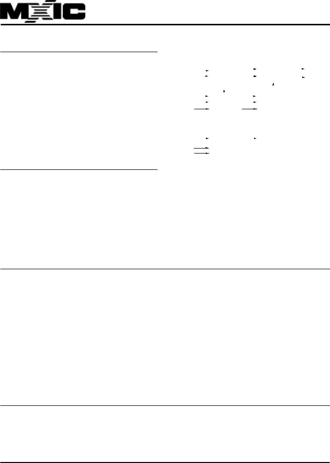
PIN DESCRIPTION |
BLOCK DIAGRAM |
|
Symbol |
Pin Function |
||||
A0~A19 |
Address Inputs |
||||
|
|
|
|
|
|
Q0~Q7 |
Data Outputs |
||||
|
|
|
|
|
|
CE/CE |
|
|
Chip Enable Input |
||
|
|
|
|
|
|
|
|
|
Output Enable Input |
||
OE/OE |
|||||
|
|
|
|
|
|
VCC |
Power Supply Pin (+5V) |
||||
|
|
|
|
|
|
VSS |
Ground Pin |
||||
|
|
|
|
|
|
|
|
|
|
|
|
|
|
|
|
|
|
|
|
|
|
|
|
|
|
|
|
CE/CE |
|
|
|
|
CONTROL |
|
OUTPUT |
|
|
|
|
Q0~Q7 |
|||||||||
|
|
|
|
|
|
|
|
|
|
|
|
|
|
|
|
|
|
|
|
|
|
OE/OE |
|
|
|
LOGIC |
|
BUFFERS |
|
|
|
|
|||||||||||
|
|
|
|
|
|
|
|
|
|||||||||||||
|
|
|
|
|
|
|
|
|
|||||||||||||
|
|
|
|
|
|
|
|
|
|
|
|
|
|
|
|
|
|||||
|
|
|
|
|
|
|
|
|
|
|
|
|
|
|
|
|
|
|
|
|
|
|
|
|
|
|
|
|
|
|
|
|
|
|
|
|
|
|
|
|
|
|
|
|
|
|
. |
|
Y-DECODER |
. |
Y-SELECT |
|
|
|
|
|
|||||||||
|
|
|
|
. |
|
|
|
|
. |
|
|
|
|
|
|
|
|||||
|
|
|
|
|
|
|
|
|
|
|
|||||||||||
A0~A19 |
|
. |
|
|
|
|
. |
|
|
|
|
|
|
|
|||||||
|
|
|
|
. |
|
|
|
|
|
|
|
||||||||||
ADDRESS |
|
|
. |
|
|
|
|
8M BIT |
|
|
|
|
|
||||||||
|
|
|
|
|
|
. |
|
|
|
|
|
||||||||||
INPUTS |
. |
|
X-DECODER |
ROM ARRAY |
|
|
|
|
|
||||||||||||
|
. |
|
|
|
|
|
|||||||||||||||
|
|
|
. |
|
|
|
|
|
|
|
|
|
|
|
|||||||
|
|
|
. |
|
|
|
|
. |
|
|
|
|
|
|
|
||||||
|
|
|
. |
|
|
|
|
. |
|
|
|
|
|
|
|
||||||
|
|
|
|
|
|
|
|
|
|
|
|
|
|
|
|
|
|
|
|
|
|
|
|
|
|
|
|
|
|
|
|
|
|
|
|
|
|
|
|
|
|
|
|
VCC
VSS
ABSOLUTE MAXIMUM RATINGS*
RATING |
VALUE |
Ambient Operating Temperature |
0°C to 70°C |
|
|
Storage Temperature |
-65°C to 125°C |
|
|
Applied Input Voltage |
-0.5V to VCC+0.5 |
|
|
Applied Output Voltage |
-0.5V to VCC+0.5 |
|
|
VCC to Ground Potential |
-0.5V to 7.0V |
|
|
Power Dissipation |
1.0W |
|
|
*Note:
Stress greater than those listed under ABSOLUTE MAXIMUM RATINGS may cause permanent damage to the device. This is a stress rating only and functional operation of the device at these or any other conditions above those indicated in the operational sections of this specification is not implied. Exposure to absolute maximum rating conditions for extended period may affect reliability.
DC CHARACTERISTICS (Ta = 0°C ~ 70°C, VCC = 5.0V ± 10%)
Item |
Symbol |
MIN. |
MAX. |
Conditions |
|
Output High Voltage |
VOH |
2.4V |
- |
IOH = -1.0mA |
|
|
|
|
|
|
|
Output Low Voltage |
VOL |
- |
0.4V |
IOL = 2.1mA |
|
|
|
|
|
|
|
Input High Voltage |
VIH |
2.2V |
VCC+0.3V |
|
|
|
|
|
|
|
|
Input Low Voltage |
VIL |
-0.3V |
0.8V |
|
|
|
|
|
|
|
|
Input Leakage Current |
ILI |
- |
10uA |
VIN=0 to 5.5V |
|
|
|
|
|
|
|
Output Leakage Current |
ILO |
- |
10uA |
VOUT=0 to 5.5V |
|
|
|
|
|
|
|
Power-Down Supply Current |
ICC3 |
- |
100uA |
|
|
CE>VCC-0.2V |
|||||
Standby Supply Current |
ICC2 |
- |
1.0mA |
|
|
CE=VIH |
|||||
Operating Supply Current |
ICC1 |
- |
40mA |
Note 1 |
|
|
|
|
|
|
|
CAPACITANCE (Ta = 25°C, f=1.0MHz (Note 2))
Item |
Symbol |
MIN. |
MAX. |
UNIT |
Conditions |
Input Capacitance |
CIN |
- |
10 |
pF |
VIN=0V |
|
|
|
|
|
|
Output Capacitance |
COUT |
- |
10 |
pF |
VOUT=0V |
|
|
|
|
|
|
P/N:PM0137 |
REV. 3.8, JUL. 16, 2001 |
2
MX23C8000
AC CHARACTERISTICS (Ta = -10°C ~ 70°C, VCC = 5.0V ± 10%)
|
|
23C8000-10 |
23C8000-12 |
23C8000-15 |
|
23C8000-20 |
|
||||||
PARAMETER |
SYMBOL |
MIN. |
MAX. |
MIN. |
MAX. |
MIN. |
MAX. |
|
MIN. |
MAX. |
CONDITIONS |
||
|
|
|
|
|
|
|
|
|
|
|
|
|
|
Cycle Time |
tCYC |
100ns |
- |
|
120ns |
- |
|
150ns |
- |
|
200ns |
- |
|
|
|
|
|
|
|
|
|
|
|
|
|
|
|
Address Access Time |
tAA |
- |
100ns |
- |
120ns |
- |
150ns |
- |
200ns |
|
|||
|
|
|
|
|
|
|
|
|
|
|
|
|
|
Output Hold Time After |
tOH |
0ns |
- |
|
0ns |
- |
|
0ns |
- |
|
0ns |
- |
|
Address Change |
|
|
|
|
|
|
|
|
|
|
|
|
|
|
|
|
|
|
|
|
|
|
|
|
|
|
|
Chip Enable Access Time |
tACE |
- |
100ns |
- |
120ns |
- |
150ns |
- |
200ns |
|
|||
|
|
|
|
|
|
|
|
|
|
|
|
|
|
Output Enable/Chip Select |
tAOE |
- |
80ns |
- |
80ns |
- |
80ns |
- |
100ns |
|
|||
Access Time |
|
|
|
|
|
|
|
|
|
|
|
|
|
|
|
|
|
|
|
|
|
|
|
|
|
|
|
Output Low Z Delay |
tLZ |
0ns |
- |
|
0ns |
- |
|
0ns |
- |
|
0ns |
- |
Note 3 |
|
|
|
|
|
|
|
|
|
|
|
|
|
|
Output High Z Delay |
tHZ |
|
20ns |
- |
20ns |
- |
20ns |
- |
20ns |
Note 4 |
|||
|
|
|
|
|
|
|
|
|
|
|
|
|
|
Note:
1.Measured with device selected at f=5MHz and output unloaded.
2.This parameter is periodically sampled and is not 100% teseted.
3.Output low-impedance delay (tLA) is measured from CE going low.
4.Output high-impedance delay (tHZ) is measured from CE going high.
AC Test Conditions
Input Pulse Levels |
0.4V~2.4V |
Input Rise and Fall Times |
10ns |
|
|
Input Timing Level |
1.5V |
|
|
Output Timing Level |
0.8V and 2.0V |
|
|
Output Load |
See Figure |
|
|
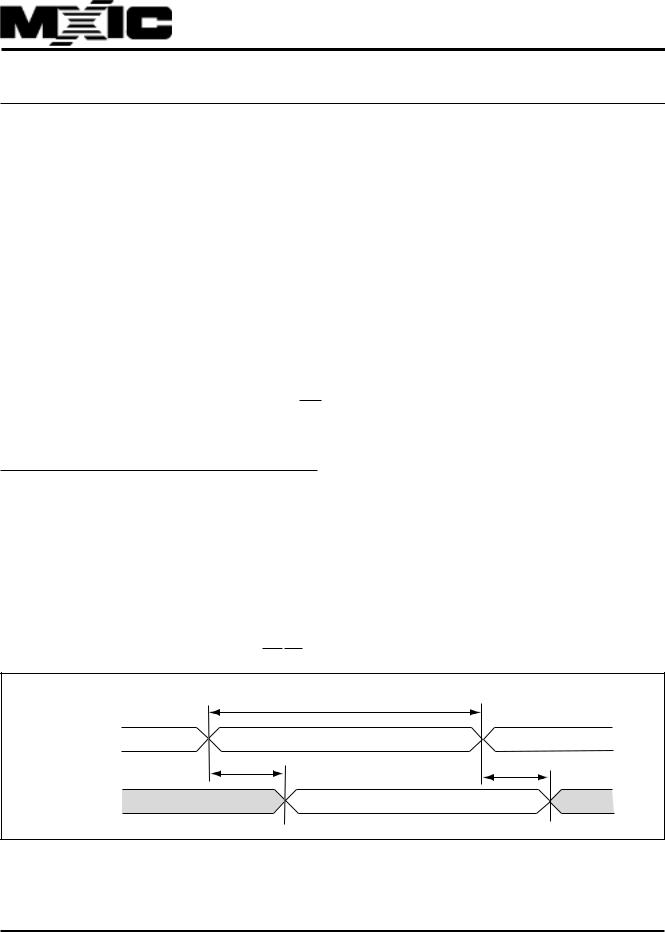
TIMING DIAGRAM
PROPAGATION DELAY FROM ADDRESS (CE/OE=ACTIVE)
|
|
tCYC |
ADDRESS |
|
VALID ADDRESS |
INPUTS |
|
|
|
tAA |
tOH |
|
|
|
DATA OUT |
|
VALID DATA |
|
|
P/N:PM0137 |
REV. 3.8, JUL. 16, 2001 |
3
 Loading...