


MCC TSMBJ0324C, TSMBJ0322C, TSMBJ0318C, TSMBJ0312C, TSMBJ0316C Datasheet
...
M C C
! "# $% ! "#
TSMBJ0306C
THRU
TSMBJ0324C
Features
∙Oxide-Glass passivated Junction
∙Bi-Directional protection in a single device
∙Surge capabilities up to 50A@10/1000us or 150A@8/20us
∙High Off-State impedance and Low On-State voltage
∙Plastic material has UL flammability classification 94V -0
Mechanical Data
∙ Case : Molded plastic
∙Polarity : None cathode band denotes
∙Approx Weight : 0.093grams
Maximum Rating
Characteristic |
|
Symbol |
|
Value |
Unit |
|
|
||||
Non-repetitive peak |
|
IPP |
|
50A |
10/1000us |
impulse current |
|
|
|||
Non-repetitive peak |
|
ITSM |
|
20A |
8.3ms, one-half |
On-state current |
|
|
cycle |
||
Operating temperature |
|
TOP |
|
-40~125oC |
|
range |
|
|
|
|
|
Junction and storage |
|
TJ, TSTG |
|
-55~150oC |
|
temperature range |
|
|
|
|
|
Thermal Resistance
Characteristic |
Symbol |
Value |
Unit |
Thermal Resistance |
RqJL |
30oC/W |
|
junction to lead |
|
|
|
Thermal Resistance |
RqJA |
120oC/W |
On recommended |
junction to ambient |
|
|
pad layout |
Typical positive |
|
|
|
temperature |
VBR/ TJ |
0.1%/oC |
|
coefficient for |
|
|
|
breakdown voltage |
|
|
|
Transient Voltage
Protection Device
75 to 320 Volts
DO-214AA (SMBJ)
H
 Cathode Band
J
|
|
|
|
|
|
|
|
|
|
|
|
|
|
|
|
|
|
|
|
|
|
|
|
|
|
|
|
|
|
|
|
|
|
|
|
|
|
|
|
|
|
|
|
|
|
|
|
|
|
|
|
|
|
|
|
|
|
|
|
|
|
|
|
|
|
|
|
|
|
|
|
|
|
|
|
|
|
|
|
|
|
|
|
|
|
|
|
|
|
|
|
|
|
|
|
|
|
|
|
|
|
|
|
|
|
|
|
|
|
|
|
|
|
|
|
|
|
|
|
|
|
|
|
|
|
|
|
|
|
|
|
|
|
|
|
|
|
|
|
|
|
|
|
|
|
|
|
|
|
|
|
|
|
|
|
|
|
|
|
|
|
|
|
|
|
|
|
|
|
|
|
|
|
|
|
|
|
|
|
|
|
|
|
|
|
|
|
|
|
|
|
|
|
|
|
|
|
|
|
|
|
|
|
|
|
|
|
|
|
|
|
|
|
|
|
|
|
|
|
|
|
|
|
|
|
|
|
|
A |
|
|
|
|
|
|
|
|
|
|
|
|
|
|
|
|
|
C |
||||
|
|
|
|
|
|
|
|
|
|
|
|
|
|
|
|
|
|
|
|
|
|
|
|
|
|
|
|
|
|
|
|
|
|
|
|
||||||
|
|
|
|
|
|
|
|
|
|
|
|
|
|
|
|
|
|
|
|
|
|
|
|
|
|
|
|
|
|
|
|
|
|
|
|
|
|
|
|
|
|
|
|
|
|
|
|
|
|
|
|
|
|
|
|
|
|
|
|
|
|
|
|
|
|
|
|
|
|
|
|
|
|
|
|
|
|
|
|
|
|
|
|
|
|
|
|
|
|
|
|
|
|
|
E |
|
|
|
|
|
D |
|
|
|
|
|
|
|
|
|
|
B |
|
|
|
|
|
|
|
|
|
||||
|
|
|
|
|
|
|
|
F |
|
|
|
|
|
|
|
|
|
|
|
|
|
|
|
|
|
|
|
|
|
|
|
|
|
||||||||
|
|
|
|
|
|
|
|
|
|
|
|
|
|
|
|
|
|
|
|
|
|
|
|
|
|
|
|
|
|
|
|
|
|
|
|||||||
|
|
|
|
|
|
|
|
|
|
|
|
|
|
|
|
|
|
|
|
|
|
|
|
|
|
|
|
|
|
|
|
|
|
|
|
|
|
|
|
||
|
|
|
|
|
|
|
|
G |
|
|
|
|
|
|
|
|
|
|
|
|
|
|
|
|
|
|
|
|
|
|
|
|
|
|
|
|
|
|
|
|
|
|
|
|
|
|
|
|
|
|
|
|
|
|
|
|
|
|
|
|
|
|
|
|
|
|
|
|
|
|
|
|
|
|
|
|
|
||||||
|
|
|
|
|
|
|
|
|
|
|
|
|
|
|
|
DIMENSIONS |
|
|
|
|
|
|
|
|
|
|
|
|
|
|
|
|
|
||||||||
|
|
|
|
|
|
|
|
INCHES |
|
|
|
|
|
|
|
|
|
|
MM |
|
|
|
|
|
|
|
|
|
|
|
|
|
|
|
|
|
|||||
|
|
DIM |
|
MIN |
|
|
|
MAX |
|
MIN |
|
MAX |
|
|
|
NOTE |
|||||||||||||||||||||||||
|
|
|
A |
.078 |
|
.096 |
|
|
2.00 |
|
|
|
|
2.44 |
|
|
|
|
|
|
|
|
|
|
|
|
|||||||||||||||
|
|
|
B |
.077 |
|
.083 |
|
|
1.96 |
|
|
|
|
2.10 |
|
|
|
|
|
|
|
|
|
|
|
|
|||||||||||||||
|
|
|
C |
.002 |
|
.008 |
|
|
|
.05 |
|
|
|
|
.20 |
|
|
|
|
|
|
|
|
|
|
|
|
||||||||||||||
|
|
|
D |
--- |
|
.02 |
|
|
|
--- |
|
|
|
|
.51 |
|
|
|
|
|
|
|
|
|
|
|
|
||||||||||||||
|
|
|
E |
.030 |
|
.060 |
|
|
.76 |
|
|
|
|
1.52 |
|
|
|
|
|
|
|
|
|
|
|
|
|||||||||||||||
|
|
|
F |
.065 |
|
.091 |
|
|
1.65 |
|
|
|
|
2.32 |
|
|
|
|
|
|
|
|
|
|
|
|
|||||||||||||||
|
|
|
G |
.205 |
|
.220 |
|
|
5.21 |
|
|
|
|
5.59 |
|
|
|
|
|
|
|
|
|
|
|
|
|||||||||||||||
|
|
|
H |
.160 |
|
.180 |
|
|
4.06 |
|
|
|
|
4.57 |
|
|
|
|
|
|
|
|
|
|
|
|
|||||||||||||||
|
|
|
J |
.130 |
|
.155 |
|
|
3.30 |
|
|
|
|
3.94 |
|
|
|
|
|
|
|
|
|
|
|
|
|||||||||||||||
SUGGESTED SOLDER
PAD LAYOUT
0.090"
0.085”
0.070”
www.mccsemi.com
TSMBJ0306C thru TSMBJ0324C M C C
ELECTRICAL CHARACTERISTIC @25 Unless otherwise specified
|
Rated |
Off-state |
Breakover |
On-State |
|
|
|
|
Off-State |
|
Parameter |
Repetitive Off- |
Leakage |
Voltage |
Breakover Current |
Holding Current |
|||||
Voltage |
Capacitance |
|||||||||
|
state Voltage |
Current@VDRM |
|
@IT =1.0A |
|
|
|
|
|
|
Symbol |
VDRM |
IDRM |
VBO |
VT |
IBO- |
IBO+ |
IH- |
IH+ |
CJ |
|
Units |
Volts |
uA |
Volts |
Volts |
mA |
mA |
mA |
mA |
pF |
|
Limit |
Max |
Max |
Max |
Max |
Min |
Max |
Min |
Max |
Typ. |
|
TSMBJ0306C |
75 |
5 |
98 |
5 |
50 |
800 |
150 |
800 |
100 |
|
TSMBJ0307C |
90 |
5 |
130 |
5 |
50 |
800 |
150 |
800 |
60 |
|
TSMBJ0310C |
140 |
5 |
180 |
5 |
50 |
800 |
150 |
800 |
60 |
|
TSMBJ0312C |
160 |
5 |
220 |
5 |
50 |
800 |
150 |
800 |
60 |
|
TSMBJ0316C |
190 |
5 |
265 |
5 |
50 |
800 |
150 |
800 |
40 |
|
TSMBJ0318C |
220 |
5 |
300 |
5 |
50 |
800 |
150 |
800 |
40 |
|
TSMBJ0322C |
275 |
5 |
350 |
5 |
50 |
800 |
150 |
800 |
40 |
|
TSMBJ0324C |
320 |
5 |
400 |
5 |
50 |
800 |
150 |
800 |
40 |
|
MAXIMUM RATED SURGE WAVEFORM
Waveform |
Standard |
Ipp (A) |
|
|
|
2/10 us |
GR-1089-CORE |
200 |
|
|
|
8/20 us |
IEC 61000-4-5 |
150 |
|
|
|
10/160 us |
FCC Part 68 |
100 |
|
|
|
10/700 us |
ITU-T K20/21 |
60 |
|
|
|
10/560 us |
FCC Part 68 |
60 |
|
|
|
10/1000 us |
GR-1089-CORE |
50 |
|
|
|
Symbol |
Parameter |
|
|
|
|
VDRM |
Stand-off voltage |
|
|
|
|
IDRM |
Leakage current at stand-off voltage |
|
|
|
|
VBR |
Breakdown voltage |
|
|
|
|
IBR |
Breakdown current |
|
|
|
|
VBO |
Breakover voltage |
|
|
|
|
IBO |
Breakover current |
|
|
|
|
IH |
Holding current |
NOTE: 1 |
|
|
|
VT |
On state voltage |
|
|
|
|
IPP |
Peak pulse current |
|
CO |
Off-state capacitance |
NOTE: 2 |
(%) |
|
|
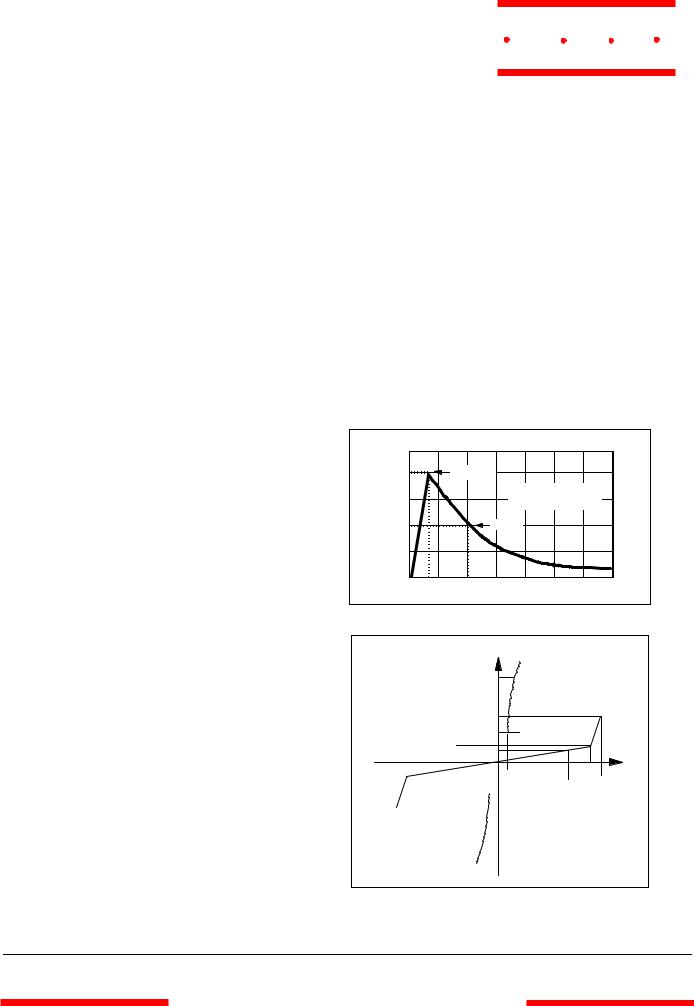
CURRENT |
100 |
Peak value(Ipp) |
|
|
tr = rise time to peak value |
PULSEPEAK;Ipp |
|
tp = decay time to half value |
50 |
Half value |
|
|
0 |
|
tr |
tp |
TIME |
|
|
|
|
I |
|
|
|
|
IPP |
|
|
|
|
IBO |
|
|
|
|
IH |
|
|
|
IBR |
IDRM |
|
|
|
|
|
V |
|
|
|
|
VBR |
|
|
|
VT |
|
|
|
|
VDRM |
VBO |
|
|
|
|
NOTE
1.I H > ( V L/ R L) If this criterion is not obeyed, the TSPD triggers but does not return correctly to high-resistance state. The surge recovery time. It does not exceed 30ms.
2.Off-state capacitance measured at f=1.0MHz , 1.0Vrms signal , VR=2Vdc bias.
www.mccsemi.com
 Loading...