


19-1181; Rev 1; 7/97
VHF-to-Microwave, +3V,
General-Purpose Amplifiers
_______________General Description
The MAX2630/MAX2631/MAX2632/MAX2633 are lowvoltage, low-noise amplifiers for use from VHF to microwave frequencies. Operating from a single +2.7V to +5.5V supply, these devices have a flat gain response to 900MHz. Their low noise figure and low supply current make them ideal for receive, buffer, and transmit IF applications.
The MAX2630/MAX2631 are biased internally, eliminating the need for external bias resistors or inductors. The MAX2632/MAX2633 have a user-selectable supply current, which can be adjusted by adding a single external resistor. This allows customized output power and gain according to specific applications requirements. The MAX2631/MAX2633 feature a shutdown pin that allows them to be powered down to less than 1µA supply current. Aside from a single bias resistor required for the MAX2632/MAX2633, the only external components needed for this family of amplifiers are input and output blocking capacitors and a VCC bypass capacitor.
The MAX2630 comes in a 4-pin SOT143 package, requiring minimal board space. The MAX2631/MAX2632 come in small 5-pin SOT23 packages. The MAX2633 comes in a 6-pin SOT23 package.
____________________________Features
♦Single +2.7V to +5.5V Operation
♦Internally Biased (MAX2630/MAX2631)
♦Adjustable Bias (MAX2632/MAX2633)
♦6.6mA Supply Current (insensitive to supply voltage)
♦1µA Shutdown Current (MAX2631/MAX2633)
♦3.7dB Noise Figure
♦13.4dB Gain
♦Ultra-Small SOT Packages
______________Ordering Information
PART |
TEMP. RANGE |
PIN- |
SOT TOP |
|
PACKAGE |
MARK* |
|||
|
|
|||
|
|
|
|
|
MAX2630EUS-T |
-40°C to +85°C |
4 SOT143 |
DG_ _ |
|
MAX2631EUK-T |
-40°C to +85°C |
5 SOT23-5 |
AABK |
|
|
|
|
|
|
MAX2632EUK-T |
-40°C to +85°C |
5 SOT23-5 |
AABL |
|
|
|
|
|
|
MAX2633EUT-T |
-40°C to +85°C |
6 SOT23-6 |
AAAA |
|
|
|
|
|
*The first two letters in the SOT top mark identify the part, while the remaining two letters are the lot-tracking code.
________________________Applications
Personal Communicating Systems |
Cordless Phones |
Global Positioning Systems |
Cellular Phones |
Wireless Local Area Networks |
ISM Radios |
Wireless Local Loops |
TV Tuners |
Land Mobile Radios |
Set-Top Boxes |
__________Typical Operating Circuit
ON |
|
|
CBLOCK |
|
|
SHDN |
BIAS |
IN |
IN |
||
|
|||||
OFF |
|
|
|||
|
|
|
|
||
|
GND |
|
RBIAS |
|
|
|
|
BIAS |
|
||
OUT |
OUT |
|
VCC |
VCC |
|
|
|
|
|||
CBLOCK |
|
MAX2633 |
CBYP |
|
_________________Pin Configurations
TOP VIEW
OUT |
3 |
4 |
VCC |
MAX2630 |
|
||
|
|
|
|
|
|
DG |
|
GND |
2 |
1 |
IN |
|
|
SOT143 |
|
BIAS |
1 |
5 |
IN |
|
|
MAX2632 |
|
GND |
2 |
AABL |
|
|
|
||
OUT |
3 |
4 |
VCC |
|
|
SOT23-5 |
|
SHDN |
1 |
MAX2631 |
5 |
IN |
|
|
|
|
|
GND |
2 |
AABK |
|
|
|
|
|
||
OUT |
3 |
|
4 |
VCC |
|
|
SOT23-5 |
|
|
SHDN |
1 |
MAX2633 |
6 |
IN |
|
|
|
|
|
GND |
2 |
AAAA |
5 |
BIAS |
|
||||
OUT |
3 |
|
4 |
VCC |
|
|
SOT23-6 |
|
|
________________________________________________________________ Maxim Integrated Products 1
MAX2633–MAX2630
For free samples & the latest literature: http://www.maxim-ic.com, or phone 1-800-998-8800. For small orders, phone 408-737-7600 ext. 3468.

MAX2630–MAX2633
VHF-to-Microwave, +3V,
General-Purpose Amplifiers
ABSOLUTE MAXIMUM RATINGS
VCC to GND ................................................................ |
|
- 0.3V to 6V |
Input Power......................................................................... |
|
5dBm |
OUT Current ..................................................................... |
|
±12mA |
IN to GND Voltage ................................................... |
|
- 1.2V to 1.2V |
Bias to GND Voltage .................................................... |
|
0.0V to 3V |
Voltage at SHDN Input |
|
|
(MAX2631/MAX2633)............................ |
-0.3V to (VCC + 0.3V) |
|
Current into SHDN Input (MAX2631/MAX2633) |
.................100µA |
|
Continuous Power Dissipation (TA = +70°C) |
|
SOT143 (derate 4mW/°C above +70°C)..................... |
320mW |
SOT23-5 (derate 7.1mW/°C above +70°C)................. |
571mW |
SOT23-6 (derate 7.1mW/°C above +70°C)................. |
571mW |
Operating Temperature Range ........................... |
-40°C to +85°C |
Junction Temperature...................................................... |
+150°C |
Storage Temperature Range ............................. |
-65°C to +150°C |
Lead Temperature (soldering, 10sec) ............................. |
+300°C |
Stresses beyond those listed under “Absolute Maximum Ratings” may cause permanent damage to the device. These are stress ratings only, and functional operation of the device at these or any other conditions beyond those indicated in the operational sections of the specifications is not implied. Exposure to absolute maximum rating conditions for extended periods may affect device reliability.
ELECTRICAL CHARACTERISTICS
(VCC = +3V, Z0 = 50Ω , fIN = 900MHz, RBIAS = 10kΩ (MAX2632/MAX2633), V SHDN = VCC (MAX2631/MAX2633), TA = +25°C, unless otherwise noted.)
PARAMETERS |
|
CONDITIONS |
MIN |
TYP |
MAX |
UNITS |
||||
|
|
|
|
|
|
|
|
|
|
|
Operating Temperature Range |
(Note 1) |
|
|
|
-40 |
|
85 |
|
degrees |
|
|
|
|
|
|
|
|
|
|
|
|
Supply Voltage |
|
|
|
|
|
2.7 |
|
5.5 |
|
V |
|
|
|
|
|
|
|
|
|
|
|
Power Gain |
|
TA = +25°C |
|
|
|
11 |
13.4 |
16.5 |
|
dB |
|
|
|
|
|
|
|
|
|
||
|
TA = TMIN to TMAX (Note 1) |
9.4 |
|
18.4 |
|
|||||
|
|
|
|
|
||||||
Noise Figure |
|
|
|
|
|
3.8 |
|
|
dB |
|
|
|
|
|
|
|
|
|
|
|
|
Output 1dB Compression Point |
|
|
|
|
|
-11 |
|
|
dBm |
|
|
|
|
|
|
|
|
|
|
|
|
Output IP3 |
|
|
|
|
|
-1 |
|
|
dBm |
|
|
|
|
|
|
|
|
|
|
|
|
Input Voltage Standing-Wave Ratio |
fIN = 800MHz to 1000MHz |
|
1.3:1 |
|
|
|
||||
Output Voltage Standing-Wave Ratio |
fIN = 800MHz to 1000MHz |
|
1.25:1 |
|
|
|
||||
|
|
RBIAS = 40kΩ |
|
|
|
|
1.3 |
1.5 |
|
|
|
|
|
VCC = 3V, TA = +25°C |
|
5.5 |
6.5 |
8.0 |
|
|
|
Supply Current |
|
RBIAS =10kΩ |
VCC = 3V, TA = TMIN to TMAX (Note1) |
|
4.2 |
6.5 |
9.2 |
|
mA |
|
|
|
|
VCC = 2.7V to 5.5V, TA = +25°C |
|
5.2 |
6.5 |
11.0 |
|
|
|
|
|
RBIAS = 500Ω |
|
|
|
15 |
17 |
|
|
|
Shutdown Supply Current |
MAX2631/MAX2633 |
|
<0.1 |
1 |
|
µA |
||||
|
|
|
|
|
|
|
|
|
|
|
SHDN Input Low Voltage |
MAX2631/MAX2633, VCC = 2.7V to 5.5V |
|
|
0.45 |
|
V |
||||
SHDN Input High Voltage |
MAX2631/MAX2633, VCC = 2.7V to 5.5V |
2.0 |
|
|
|
V |
||||
SHDN Input Bias Current |
MAX2631/ |
|
VSHDN = VCC |
|
|
30 |
|
µA |
||
MAX2633 |
|
VSHDN = GND |
|
|
1 |
|
||||
|
|
|
|
|
|
|
||||
|
|
|
|
|
|
|
|
|
|
|
Note 1: Guaranteed by design and characterization.
2 _______________________________________________________________________________________ 


VHF-to-Microwave, +3V,
General-Purpose Amplifiers
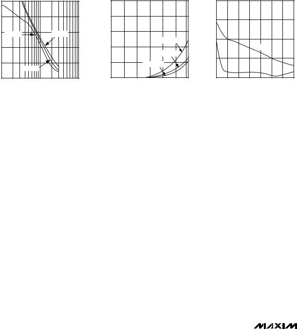
__________________________________________Typical Operating Characteristics
(VCC = +3V, V SHDN = VCC (MAX2631/MAX2633), Z0 = 50Ω , fIN = 900MHz, RBIAS = 10kΩ (MAX2632/MAX2633), TA = +25°C, unless otherwise noted.)
SUPPLY CURRENT vs. SUPPLY VOLTAGE |
MAX2632/MAX2633 |
|
GAIN vs. SUPPLY CURRENT |
GAIN vs. FREQUENCY AND VOLTAGE |
|
10 |
|
|
|
MAX2630-1 |
|
25 |
|
|
|
|
|
MAX2630-2 |
|
20 |
|
|
|
|
|
|
MAX2632-3 |
|
|
TA = +85°C |
|
|
|
|
|
|
|
|
|
|
|
|
|
|
|
|
|
|||
|
|
|
|
|
|
|
|
|
|
|
|
|
|
|
|
|
|
|
|
|
|
|
|
8 |
|
|
|
|
|
20 |
|
|
|
f = 0.1GHz |
|
|
16 |
|
|
|
|
|
|
|
|
|
|
|
|
|
|
|
|
|
|
|
|
|
|
|
|
|
|
|
|
|
VCC = 5V |
|
(mA) |
6 |
TA = +25°C |
|
TA = -40°C |
|
(dB) |
15 |
|
|
|
f = 0.9GHz |
|
(dB) |
12 |
|
|
|
VCC = 3V |
|
|
|
|
|
|
|
|
|
|
|
|
|
|
|
|
|
|
|
|
|
|
|
||||
I |
|
|
|
|
|
GAIN |
|
|
|
|
|
|
|
GAIN |
|
|
|
|
|
|
|
|
CC |
4 |
|
|
|
|
|
|
|
|
|
|
|
|
|
|
|
|
|
|
|
|
|
|
|
|
|
|
|
10 |
|
|
|
|
|
|
|
8 |
|
|
|
|
|
|
|
|
|
|
|
|
|
|
|
|
|
|
|
f = 1.5GHz |
|
|
|
|
|
|
|
|
|
|
|
|
2 |
|
|
|
|
|
5 |
|
|
|
|
|
|
|
4 |
|
|
|
|
|
|
|
|
0 |
|
|
|
|
|
0 |
|
|
|
|
|
|
|
0 |
|
|
|
|
|
|
|
|
2 |
3 |
4 |
5 |
6 |
|
0 |
2.5 |
5.0 |
7.5 |
10.0 |
12.5 |
15.0 |
|
0.1 |
0.3 |
0.5 |
0.7 |
0.9 |
1.1 |
1.3 |
1.5 |
|
|
VCC (V) |
|
|
|
|
|
|
ICC (mA) |
|
|
|
|
|
|
FREQUENCY (GHz) |
|
|
||||
GAIN vs. FREQUENCY |
OUTPUT 1dB COMPRESSION |
OUTPUT 1dB COMPRESSION |
AND TEMPERATURE |
POWER vs. FREQUENCY AND VOLTAGE |
POWER vs. FREQUENCY AND TEMPERATURE |
|
20 |
|
|
|
|
|
|
MAX2630-4 |
|
-5.0 |
|
|
|
|
|
|
MAX2630-5 |
|
-5.0 |
|
|
|
|
|
|
MAX2630-6 |
|
|
|
|
TA = -40°C |
|
|
|
|
|
|
|
|
|
|
|
|
|
|
|
|
|
|
||||
|
16 |
|
|
|
|
|
|
|
|
|
|
|
|
|
|
|
|
|
|
|
|
|
|
|
||
|
|
|
|
|
|
|
|
|
-7.5 |
|
|
|
|
|
|
|
|
-7.5 |
|
|
|
|
|
|
|
|
|
|
|
|
|
|
|
|
|
|
|
|
|
|
|
|
|
|
|
|
|
|
|
|
|
||
(dB) |
12 |
TA = +25°C |
|
|
|
|
|
(dBm) |
|
|
|
|
VCC = 5V |
|
|
(dBm) |
|
|
|
|
|
|
|
|
||
|
|
|
TA = +85°C |
|
|
|
-10.0 |
|
|
|
|
|
-10.0 |
|
|
|
|
|
|
|
||||||
GAIN |
|
|
|
|
|
|
P |
|
|
|
|
|
|
|
P |
|
|
|
|
|
|
|
||||
|
|
|
|
|
|
|
|
|
1- |
|
|
|
|
|
|
|
|
1- |
|
|
|
|
|
|
|
|
|
8 |
|
|
|
|
|
|
|
|
|
|
|
|
|
|
|
|
|
|
|
|
|
|
TA = +85°C |
|
|
|
|
|
|
|
|
|
|
|
|
|
|
|
VCC = 3V |
|
|
|
|
|
|
|
|
|
|
|||
|
|
|
|
|
|
|
|
|
|
-12.5 |
|
|
|
|
|
|
|
|
|
|
TA = -40°C |
|
|
|||
|
4 |
|
|
|
|
|
|
|
|
|
|
|
|
|
|
|
|
-12.5 |
|
|
|
|
|
|||
|
|
|
|
|
|
|
|
|
|
|
|
|
|
|
|
|
|
|
|
|
|
|
|
|
|
|
|
0 |
|
|
|
|
|
|
|
|
-15.0 |
|
|
|
|
|
|
|
|
-15.0 |
|
|
|
|
|
|
|
|
0.1 |
0.3 |
0.5 |
0.7 |
0.9 |
1.1 |
1.3 |
1.5 |
|
0.1 |
0.3 |
0.5 |
0.7 |
0.9 |
1.1 |
1.3 |
1.5 |
|
0.1 |
0.3 |
0.5 |
0.7 |
0.9 |
1.1 |
1.3 |
1.5 |
|
|
|
FREQUENCY (GHz) |
|
|
|
|
|
FREQUENCY (GHz) |
|
|
|
|
|
FREQUENCY (GHz) |
|
|
|||||||||
MAX2632/MAX2633 |
|
OUTPUT 1dB COMPRESSION |
NOISE FIGURE vs. FREQUENCY |
POWER vs. SUPPLY CURRENT |
|
0 |
|
|
|
|
|
MAX2630-7 |
|
5 |
|
|
|
|
|
|
MAX2630-8 |
|
|
|
|
|
|
|
|
|
|
|
|
|
|
|
||
|
-4 |
|
|
f = 0.1GHz |
|
|
|
|
4 |
|
|
|
|
|
|
|
(dBm) |
-8 |
|
f = 0.9GHz |
|
|
|
(dB) |
3 |
|
|
|
|
|
|
|
|
|
|
|
|
|
|
FIGURE |
|
|
|
|
|
|
|
|||
|
|
|
|
|
f = 1.5GHz |
|
|
|
|
|
|
|
|
|
||
-1 |
|
|
|
|
|
|
|
|
|
|
|
|
|
|
||
P |
-12 |
|
|
|
|
|
|
NOISE |
2 |
|
|
|
|
|
|
|
|
|
|
|
|
|
|
|
|
|
|
|
|
|
|
||
|
-16 |
|
|
|
|
|
|
|
1 |
|
|
|
|
|
|
|
|
-20 |
|
5.0 |
|
10.0 |
|
|
|
0 |
|
|
|
|
|
|
|
|
0 |
2.5 |
7.5 |
12.5 |
15.0 |
|
0.1 |
0.3 |
0.5 |
0.7 |
0.9 |
1.1 |
1.3 |
1.5 |
||
|
|
|
|
ICC (mA) |
|
|
|
|
|
|
FREQUENCY (GHz) |
|
|
|||
MAX2633–MAX2630
_______________________________________________________________________________________ 3
MAX2630–MAX2633
VHF-to-Microwave, +3V,
General-Purpose Amplifiers
____________________________Typical Operating Characteristics (continued)
(VCC = +3V, V SHDN = VCC (MAX2631/MAX2633), Z0 = 50Ω , fIN = 900MHz, RBIAS = 10kΩ (MAX2632/MAX2633), TA = +25°C, unless otherwise noted.)
MAX2632/MAX2633
SUPPLY CURRENT vs. RBIAS
|
15 |
|
|
|
-9 |
0.05 |
|
|
|
|
|
MAX2630 |
|
|
12 |
|
|
|
|
0.04 |
|
|
|
|
|
(μA) |
|
(mA) |
9 |
VCC = 3V |
|
VCC = 5V |
CC |
0.03 |
|
|
I |
|
|||
|
|
|
|
|
||
CC |
|
|
|
|
SHUTDOWN |
|
I |
6 |
|
|
|
0.02 |
|
|
|
|
|
|
||
|
3 |
|
|
|
|
0.01 |
|
|
|
VCC = 4V |
|
|
|
|
0 |
1 |
10 |
|
100 |
0 |
|
|
|
|
|||
|
|
|
RBIAS (kΩ) |
|
|
|
MAX2631/MAX2633 |
|
SHUTDOWN SUPPLY CURRENT |
VOLTAGE STANDING-WAVE |
vs. TEMPERATURE |
RATIO vs. FREQUENCY |
|
|
|
|
|
|
MAX2630 toc11 |
|
5:1 |
|
|
|
|
|
|
MAX2630-10 |
|
|
|
|
|
|
|
|
|
|
|
|
|
|
||
|
|
|
|
|
|
|
|
4:1 |
|
|
|
|
|
|
|
|
|
|
|
VCC = 5.5V |
|
VSWR |
3:1 |
|
|
|
|
|
|
|
|
|
|
|
|
|
|
|
|
|
|
|
|
OUT |
|
|
|
|
|
|
|
VCC = 3.0V |
|
|
2:1 |
|
|
|
|
|
|
|
|
|
|
|
|
|
|
|
|
|
|
|
|
|
|
|
|
|
|
|
VCC = 2.7V |
|
|
|
|
|
|
|
IN |
|
|
|
|
|
|
|
|
|
|
|
|
|
|
|
|
|
|
|
|
|
|
|
|
|
|
|
|
1:1 |
|
|
|
|
|
|
|
-40 |
-20 |
0 |
20 |
40 |
60 |
80 |
|
0.1 |
0.3 |
0.5 |
0.7 |
0.9 |
1.1 |
1.3 |
1.5 |
|
|
TEMPERATURE (°C) |
|
|
|
|
|
FREQUENCY (GHz) |
|
|
|||||
______________________________________________________________Pin Description
|
PIN |
|
|
|
||
|
|
|
|
NAME |
FUNCTION |
|
MAX2630 |
MAX2631 |
MAX2632 |
MAX2633 |
|||
|
|
|||||
|
|
|
|
|
|
|
1 |
5 |
5 |
6 |
IN |
Amplifier Input. Use a series blocking capacitor with less than |
|
3Ω reactance at your lowest operating frequency. |
||||||
|
|
|
|
|
||
|
|
|
|
|
|
|
2 |
2 |
2 |
2 |
GND |
Ground Connection. For optimum performance, provide a low- |
|
inductance connection to the ground plane. |
||||||
|
|
|
|
|
||
|
|
|
|
|
|
|
|
|
|
|
|
Amplifier Output. Use a series blocking capacitor with less than |
|
3 |
3 |
3 |
3 |
OUT |
||
3Ω reactance at your lowest operating frequency. |
||||||
|
|
|
|
|
||
|
|
|
|
|
|
|
|
|
|
|
|
Supply Connection. Bypass directly at the supply pin. The value |
|
|
|
|
|
|
||
|
|
|
|
|
of the bypass capacitor is determined by the lowest operating |
|
4 |
4 |
4 |
4 |
VCC |
frequency, and is typically the same as the blocking capacitor |
|
|
|
|
|
|
value. Additional bypassing may be necessary for long VCC |
|
|
|
|
|
|
lines. |
|
|
|
|
|
|
|
|
|
|
|
|
|
Shutdown Input. Driving SHDN with a logic low turns off the |
|
— |
1 |
— |
1 |
SHDN |
||
amplifier. |
||||||
|
|
|
|
|
||
|
|
|
|
|
|
|
|
|
|
|
|
Bias Resistor Connection. Connect a resistor to GND to set the |
|
— |
— |
1 |
5 |
BIAS |
bias current. See the Supply Current vs. RBIAS graph in the |
|
|
|
|
|
|
Typical Operating Characteristics. |
|
|
|
|
|
|
|
|
4 _______________________________________________________________________________________
 Loading...