


MAX197BMYI
Maxim MAX197BMYI, MAX197BEWI, MAX197BENI, MAX197BEAI, MAX197BCWI Datasheet
...
_______________General Description
The MAX197 multi-range, 12-bit data-acquisition sys-
tem (DAS) requires only a single +5V supply for opera-
tion, yet accepts signals at its analog inputs that may
span both above the power-supply rail and below
ground. This system provides 8 analog input channels
that are independently software programmable for a
variety of ranges: ±10V, ±5V, 0V to +10V, or 0V to +5V.
This increases effective dynamic range to 14 bits, and
provides the user flexibility to interface 4mA-to-20mA,
±12V, and ±15V powered sensors to a single +5V sys-
tem. In addition, the converter is overvoltage tolerant to
±16.5V; a fault condition on any channel will not affect
the conversion result of the selected channel. Other
features include a 5MHz bandwidth track/hold, a
100ksps throughput rate, software-selectable internal or
external clock and acquisition, 8+4 parallel interface,
and an internal 4.096V or an external reference.
A hardware SHDN pin and two programmable power-
down modes (STBYPD, FULLPD) are provided for low-
current shutdown between conversions. In STBYPD
mode, the reference buffer remains active, eliminating
start-up delays.
The MAX197 employs a standard microprocessor (µP)
interface. A three-state data I/O port is configured to
operate with 8-bit data buses, and data-access and
bus-release timing specifications are compatible with
most popular µPs. All logic inputs and outputs are
TTL/CMOS compatible.
The MAX197 is available in 28-pin DIP, wide SO, SSOP,
and ceramic SB packages.
For a different combination of ranges (±4V, ±2V, 0V to
4V, 0V to 2V), see the MAX199 data sheet. For 12-bit bus
interface, see the MAX196 and MAX198 data sheets.
________________________Applications
Industrial-Control Systems
Robotics
Data-Acquisition Systems
Automatic Testing Systems
Medical Instruments
Telecommunications
____________________________Features
♦ 12-Bit Resolution, 1/2LSB Linearity
♦ Single +5V Operation
♦ Software-Selectable Input Ranges:
±10V, ±5V, 0V to 10V, 0V to 5V
♦ Fault-Protected Input Multiplexer (±16.5V)
♦ 8 Analog Input Channels
♦ 6µs Conversion Time, 100ksps Sampling Rate
♦ Internal or External Acquisition Control
♦ Internal 4.096V or External Reference
♦ Two Power-Down Modes
♦ Internal or External Clock
MAX197
Multi-Range (±10V, ±5V, +10V, +5V),
Single +5V, 12-Bit DAS with 8+4 Bus Interface
________________________________________________________________
Maxim Integrated Products
1
28
27
26
25
24
23
22
21
20
19
18
17
16
15
1
2
3
4
5
6
7
8
9
10
11
12
13
14
DGND
V
DD
REF
REFADJ
INT
CH7
AGND
CH6
CH5
CH4
CH3
CH2
CH1
CH0
D0/D8
D1/D9
D2/D10
D3/D11
D4
D5
D6
D7
SHDN
HBEN
RD
WR
CS
CLK
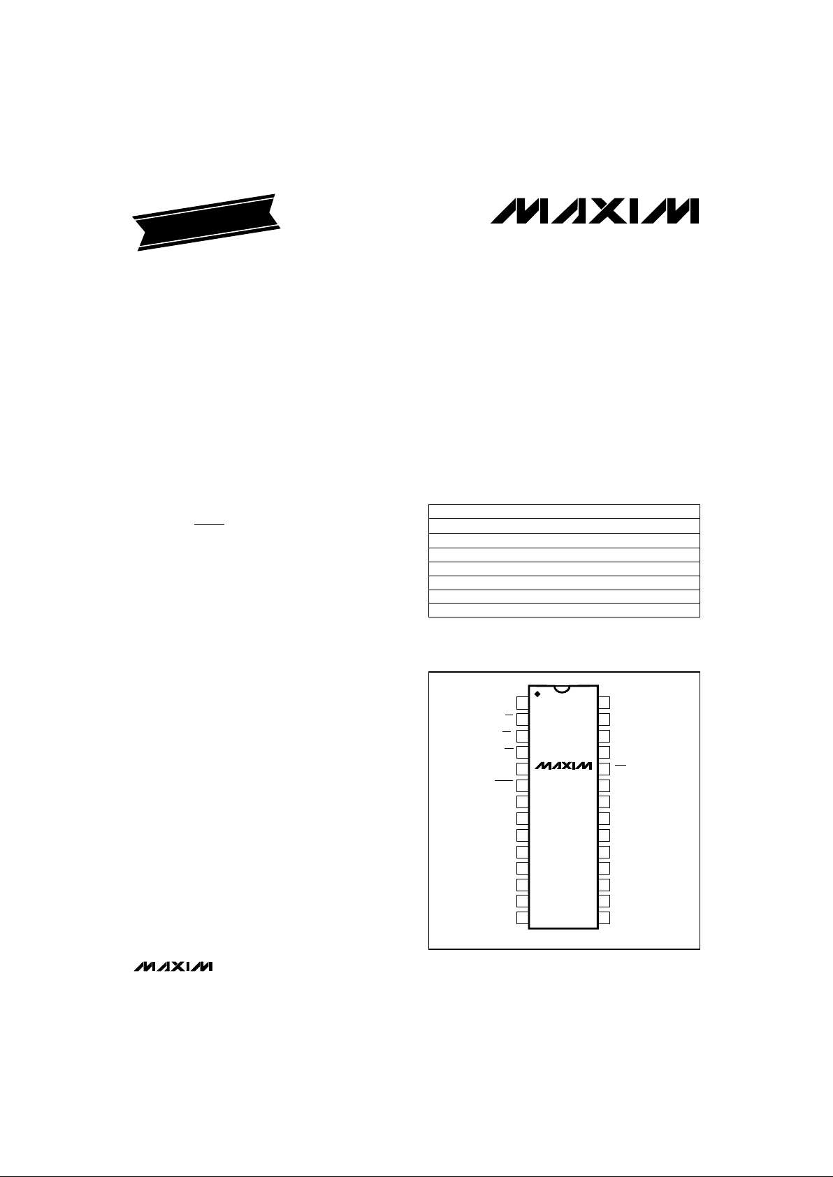
DIP/SO/SSOP/Ceramic SB
TOP VIEW
MAX197
__________________Pin Configuration
19-0381; Rev 1; 6/96
PART
MAX197ACNI
MAX197BCNI
MAX197ACWI 0°C to +70°C
0°C to +70°C
0°C to +70°C
TEMP. RANGE PIN-PACKAGE
28 Narrow Plastic DIP
28 Narrow Plastic DIP
28 Wide SO
______________Ordering Information
MAX197BCWI 0°C to +70°C 28 Wide SO
MAX197ACAI 0°C to +70°C 28 SSOP
MAX197BCAI 0°C to +70°C 28 SSOP
MAX197BC/D 0°C to +70°C Dice*
Functional Diagram appears at end of data sheet.
Ordering Information continued at end of data sheet.
*Dice are specified at T
A
= +25°C, DC parameters only.
EVALUATION KIT
MANUAL AVAILABLE
For free samples & the latest literature: http://www.maxim-ic.com, or phone 1-800-998-8800
MAX197
Multi-Range (±10V, ±5V, +10V, +5V),
Single +5V, 12-Bit DAS with 8+4 Bus Interface
2 _______________________________________________________________________________________
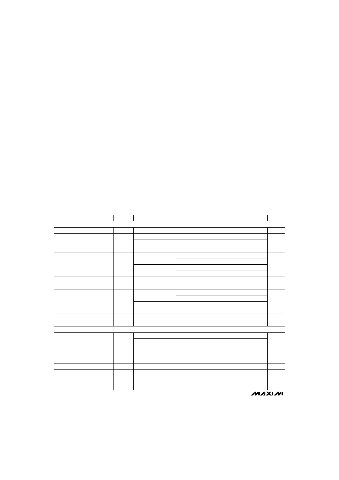
ABSOLUTE MAXIMUM RATINGS
ELECTRICAL CHARACTERISTICS
(V
DD
= 5V ±5%; unipolar/bipolar range; external reference mode, V
REF
= 4.096V; 4.7µF at REF pin; external clock, f
CLK
= 2.0MHz
with 50% duty cycle; T
A
= T
MIN
to T
MAX
, unless otherwise noted.)
Stresses beyond those listed under “Absolute Maximum Ratings” may cause permanent damage to the device. These are stress ratings only, and functional
operation of the device at these or any other conditions beyond those indicated in the operational sections of the specifications is not implied. Exposure to
absolute maximum rating conditions for extended periods may affect device reliability.
V
DD
to AGND............................................................-0.3V to +7V
AGND to DGND.....................................................-0.3V to +0.3V
REF to AGND..............................................-0.3V to (V
DD
+ 0.3V)
REFADJ to AGND.......................................-0.3V to (V
DD
+ 0.3V)
Digital Inputs to DGND...............................-0.3V to (V
DD
+ 0.3V)
Digital Outputs to DGND............................-0.3V to (V
DD
+ 0.3V)
CH0–CH7 to AGND ..........................................................±16.5V
Continuous Power Dissipation (T
A
= +70°C)
Narrow Plastic DIP (derate 14.29mW/°C above +70°C)....1143mW
Wide SO (derate 12.50mW/°C above +70°C)..............1000mW
SSOP (derate 9.52mW/°C above +70°C) ......................762mW
Narrow Ceramic SB (derate 20.00mW/°C above +70°C)..1600mW
Operating Temperature Ranges
MAX197_C_ _ .......................................................0°C to +70°C
MAX197_E_ _.....................................................-40°C to +85°C
MAX197_M_ _..................................................-55°C to +125°C
Storage Temperature Range.............................-65°C to +150°C
Lead Temperature (soldering, 10sec).............................+300°C
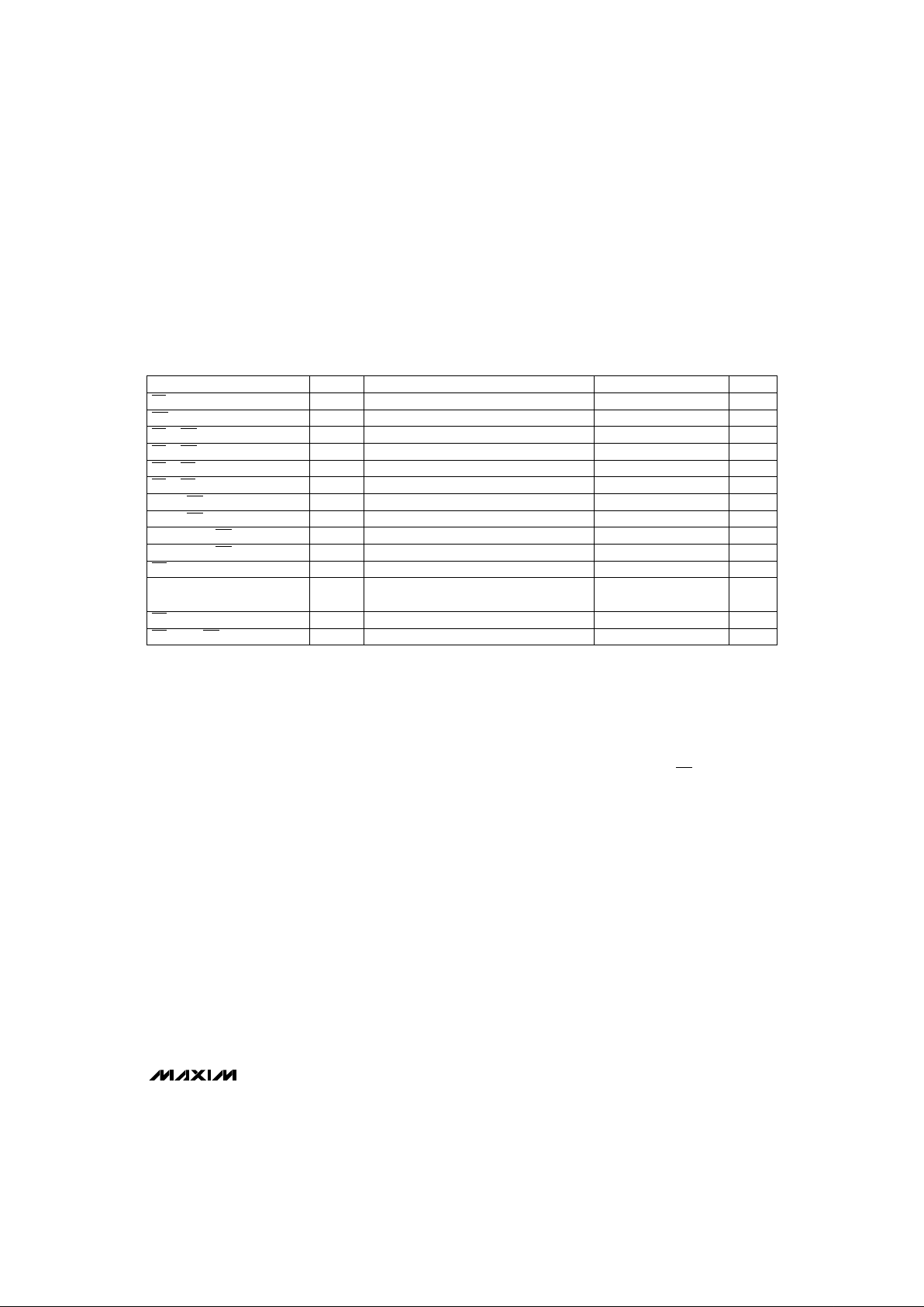
MAX197A
Internal CLK mode/internal acquisition
control (Note 4)
External CLK mode/external acquisition
control
External CLK mode/external acquisition control
50kHz, V
IN
= ±5V (Note 3)
Bipolar
Unipolar
Up to the 5th harmonic
Bipolar
MAX197B
Unipolar
CONDITIONS
10
ps<50
Aperture Jitter
ns15Aperture Delay
dB-86Channel-to-Channel Crosstalk
dB80SFDRSpurious-Free Dynamic Range
dB-85 -78THDTotal Harmonic Distortion
dB
70
LSB
±1/2
INLIntegral Nonlinearity
Bits12Resolution
±0.5
LSB
±0.1
Channel-to-Channel Offset
Error Matching
±10
±5
±1
LSB±1DNLDifferential Nonlinearity
LSB
±3
Offset Error
±5
UNITSMIN TYP MAXSYMBOLPARAMETER
MAX197A
MAX197B
MAX197A
MAX197B
Bipolar
Unipolar
Bipolar
Unipolar
5
ppm/°C
3
Gain Temperature Coefficient
(Note 2)
±10
MAX197A
±7
MAX197B
MAX197A
MAX197B
LSB
±7
Gain Error
(Note 2)
±10
69
SINADSignal-to-Noise + Distortion Ratio
ACCURACY (Note 1)
DYNAMIC SPECIFICATIONS (10kHz sine-wave input, ±10Vp-p, f
SAMPLE
= 100ksps)
MAX197A
MAX197B
ns
MAX197
Multi-Range (±10V, ±5V, +10V, +5V),
Single +5V, 12-Bit DAS with 8+4 Bus Interface
_______________________________________________________________________________________ 3
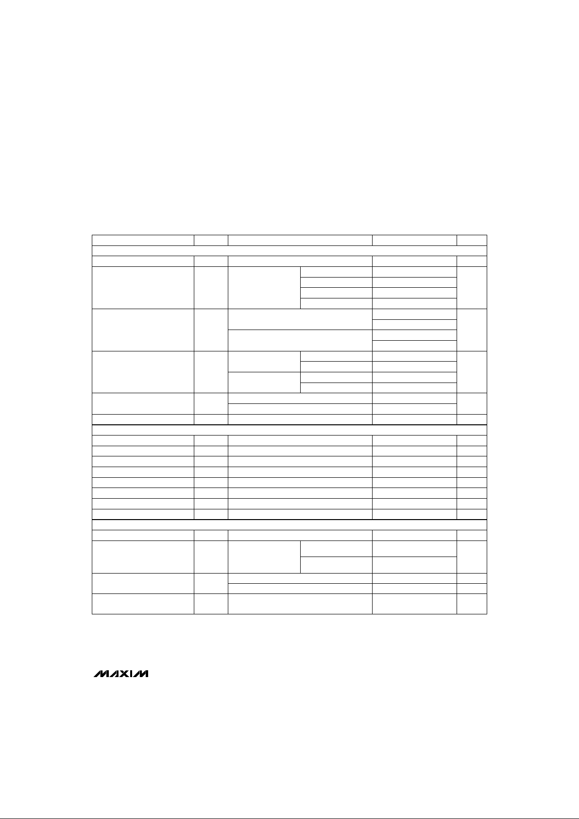
ELECTRICAL CHARACTERISTICS (continued)
(V
DD
= 5V ±5%; unipolar/bipolar range; external reference mode, V
REF
= 4.096V; 4.7µF at REF pin; external clock, f
CLK
= 2.0MHz
with 50% duty cycle; T
A
= T
MIN
to T
MAX
, unless otherwise noted.)
f
CLK
= 2.0MHz
T
A
= +25°C
(Note 5)
Unipolar
CONDITIONS
mA30Output Short-Circuit Current
ppm/°C40REF Output Tempco
V4.076 4.096 4.116V
REF
REF Output Voltage
pF40Input Capacitance
µs3Track/Hold Acquisition Time
05
V
010
Input Voltage Range
(See Table 1)
1.25
-3dB rolloff
2.5
UNITSMIN TYP MAXSYMBOLPARAMETER
MHz
5
Small-Signal Bandwidth
2.5
Bipolar
Unipolar
-600 360
0V to 10V range
-1200 720
0V to 5V range
-10V to 10V range
-5V to 5V range
Bipolar
µA
720
Input Current
Unipolar
360
16
kΩ
21
Input Dynamic Resistance
Bipolar
-5 5
-10 10
0mA to 0.5mA output current (Note 6) mV7.5Load Regulation
V2.465 2.500 2.535REFADJ Output Voltage
µF4.7Capacitive Bypass at REF
With recommended circuit (Figure 1) %±1.5REFADJ Adjustment Range
V/V1.6384Buffer Voltage Gain
V2.4 4.18Input Voltage Range
µA
400
Input Current V
REF
= 4.18V
1
VV
DD
- 50mV
REFADJ Threshold for
Buffer Disable
Normal or STANDBY power-down mode kΩ10
Input Resistance
FULL power-down mode 5 MΩ
ANALOG INPUT
INTERNAL REFERENCE
REFERENCE INPUT (Buffer disabled, reference input applied to REF pin)
±10V range
±5V range
0V to 10V range
0V to 5V range
Normal or STANDBY
power-down mode
FULL power-down
mode
TC V
REF
MAX197
Multi-Range (±10V, ±5V, +10V, +5V),
Single +5V, 12-Bit DAS with 8+4 Bus Interface
4 _______________________________________________________________________________________
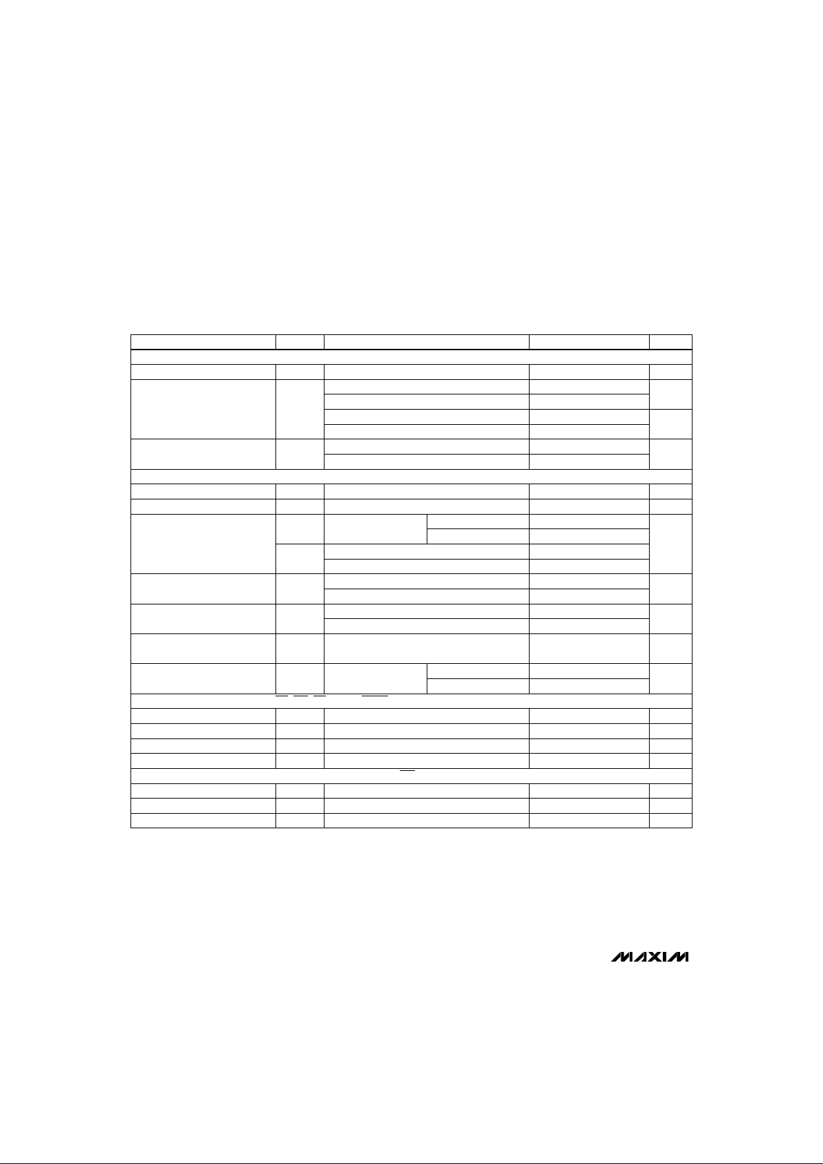
ELECTRICAL CHARACTERISTICS (continued)
(V
DD
= 5V ±5%; unipolar/bipolar range; external reference mode, V
REF
= 4.096V; 4.7µF at REF pin; external clock, f
CLK
= 2.0MHz
with 50% duty cycle; T
A
= T
MIN
to T
MAX
, unless otherwise noted.)
Internal acquisition
3.0 5.0
External reference = 4.096V
After FULLPD or STBYPD
External acquisition (Note 9)
CONDITIONS
Full power-down mode (FULLPD) (Note 7)
5
µs
3.0
t
ACQI
Acquisition Time
LSB
±
1
/
2
PSRR
Power-Supply Rejection Ratio
(Note 8)
3.0
t
ACQE
External CLK
µs
V4.75 5.25V
DD
Supply Voltage
6.0
t
CONV
Conversion Time
Internal CLK, C
CLK
= 100pF 6.0 7.7 10.0
To 0.1mV REF bypass
capacitor fully discharged
ms
8
Reference Buffer Settling
120
60
Normal mode, bipolar ranges
700 850
Normal mode, unipolar ranges
UNITSMIN TYP MAXSYMBOLPARAMETER
Standby power-down (STBYPD)
mA
18
I
DD
Supply Current
610
µA
Internal reference ±
1
/
2
C
CLK
= 100pF MHz1.25 1.56 2.00f
CLK
Internal Clock Frequency
0.1 2.0f
CLK
External Clock Frequency Range MHz
External CLK
Internal CLK
Power-up (Note 10) µs200
Bandgap Reference
Start-Up Time
External CLK
ksps
100
Throughput Rate
Internal CLK, C
CLK
= 100pF 62
C
REF
= 4.7µF
C
REF
= 33µF
V2.4V
INH
Input High Voltage
V0.8V
INL
Input Low Voltage
V
IN
= 0V or V
DD
µA±10I
IN
Input Leakage Current
(Note 5) pF15C
IN
Input Capacitance
V
DD
= 4.75V, I
SINK
= 1.6mA V0.4V
OL
Output Low Voltage
V
DD
= 4.75V, I
SOURCE
= 1mA VV
DD
- 1V
OH
Output High Voltage
(Note 5) pF15C
OUT
Three-State Output Capacitance
POWER REQUIREMENTS
TIMING
DIGITAL INPUTS (D7–D0, CLK, RD, WR, CS, HBEN, SHDN) (Note 11)
DIGITAL OUTPUTS (D7–D4, D3/D11, D2/D10, D1/D9, D0/D8, INT)
MAX197
Multi-Range (±10V, ±5V, +10V, +5V),
Single +5V, 12-Bit DAS with 8+4 Bus Interface
_______________________________________________________________________________________ 5
Note 1: Accuracy specifications tested at V
DD
= 5.0V. Performance at power-supply tolerance limits guaranteed by Power-Supply
Rejection test. Tested for the ±10V input range.
Note 2: External reference: V
REF
= 4.096V, offset error nulled, ideal last code transition = FS - 3/2LSB.
Note 3: Ground "on" channel; sine wave applied to all "off" channels.
Note 4: Maximum full-power input frequency for 1LSB error with 10ns jitter = 3kHz.
Note 5: Guaranteed by design. Not tested.
Note 6: Use static loads only.
Note 7: Tested using internal reference.
Note 8: PSRR measured at full-scale.
Note 9: External acquisition timing: starts at data valid at ACQMOD = low control byte; ends at rising edge of WR
with ACQMOD
= high control byte.
Note 10: Not subject to production testing. Provided for design guidance only.
Note 11: All input control signals specified with t
R
= t
F
= 5ns from a voltage level of 0.8V to 2.4V.
Note 12: t
DO
and t
DO1
are measured with the load circuits of Figure 2 and defined as the time required for an output to cross 0.8V
or 2.4V.
Note 13: t
TR
is defined as the time required for the data lines to change by 0.5V.
TIMING CHARACTERISTICS
(V
DD
= 5V ±5%; unipolar/bipolar range; external reference mode, V
REF
= 4.096V; 4.7µF at REF pin; external clock, f
CLK
= 2.0MHz
with 50% duty cycle; T
A
= T
MIN
to T
MAX
, unless otherwise noted.)
(Note 13) ns
70
CONDITIONS
t
TR
RD High to Output Disable
ns120t
INT1
RD Low to INT High Delay
ns80t
CS
CS Pulse Width
UNITSMIN TYP MAXSYMBOLPARAMETER
ns80t
WR
WR Pulse Width
ns0t
CSWS
ns0t
CSWH
CS to WR Hold Time
CS to WR Setup Time
ns0t
CSRS
ns0t
CSRH
CS to RD Hold Time
CS to RD Setup Time
ns100t
CWS
ns50t
CWH
CLK to WR Hold Time
CLK to WR Setup Time
ns60t
DS
ns0t
DH
Data Valid to WR Hold
Data Valid to WR Setup
Figure 2, C
L
= 100pF (Note 12)
Figure 2, C
L
= 100pF (Note 12)
ns120t
DO
ns120t
DO1
HBEN High or HBENLow to
Output Valid
RD Low to Output Data Valid
 Loading...