


19-0879; Rev 0; 7/07
+5.0V, ±15kV ESD-Protected, Half-Duplex/ Full-Duplex, RS-485 Transceiver in µDFN
General Description
The MAX13181E–MAX13184E are full-duplex and selectable half-/full-duplex RS-485 transceivers in a tiny 2mm x 2mm µDFN package. These devices are designed for space-constrained applications by including extended ESD protection to ±15kV per Human Body Model (HBM) and integrating pullup/pulldown resistors on the DE, RE and H/F inputs to reduce external components. The MAX13182E/MAX13184E feature a low-current shutdown mode for power-sensitive applications.
These devices have a 1/8 unit-load input receiver that allows up to 256 transceivers on the bus. The MAX13181E/MAX13182E feature reduced slew-rate drivers to minimize EMI and reflections that are caused by improperly terminated cables. The slew-rate limited MAX13181E/MAX13182E allow error-free data transmission up to 250kbps. The MAX13183E/MAX13184E feature full-speed drivers, allowing data rates of up to 16Mbps. The MAX13182E/MAX13184E are configured for fullduplex operation, while the MAX13181E/MAX13183E feature pin-selectable halfor full-duplex operation. All driver outputs and receiver inputs include extended ESD protection.
The MAX13181E–MAX13184E are available in a tiny 10pin, 2mm x 2mm µDFN. The MAX13183E/MAX13184E are also available in industry-standard 14-pin SO packages. The devices operate over the extended -40°C to +85°C temperature range.
|
Applications |
Industrial Control |
Security System |
Motor Drive Control |
Instrumentation |
Telecom |
|
Features
♦Available in Tiny, 10-Pin, 2mm x 2mm, µDFN and 14-Pin SO Packages
♦+5.0V Operation
♦Extended ESD Protection
±15kV Human Body Model
±12kV IEC 61000-4-2 Air-Gap Disharge ±6kV IEC 61000-4-2 Contact Disharge
♦Slew-Rate Limiting Facilitates Error-Free Data Transmission (MAX13181E/MAX13182E)
♦2.5µA (typ) Low-Current Shutdown Mode
♦1/8-Unit Load Allows Up to 256 Transceivers on the Bus
Pin Configurations
TOP VIEW |
|
|
|
|
|
|
|
|
|
A |
B |
Z |
Y |
GND |
A |
B |
Z |
Y |
GND |
10 |
9 |
8 |
7 |
6 |
10 |
9 |
8 |
7 |
6 |
|
MAX13181E |
|
|
MAX13182E |
|
||||
+ |
MAX13183E |
|
+ |
MAX13184E |
|
||||
|
|
|
|
|
|
|
|
||
1 |
2 |
3 |
4 |
5 |
1 |
2 |
3 |
4 |
5 |
VCC |
RO |
H/F |
DE |
DI |
VCC |
RO |
RE |
DE |
DI |
|
|
µDFN |
|
|
|
|
µDFN |
|
|
Pin Configurations continued at end of data sheet.
Selector Guide
PART |
HALF/FULL |
MAXIMUM DATA |
SLEW-RATE |
LOW-POWER |
RECEIVER |
|
DUPLEX |
RATE |
LIMITED |
SHUTDOWN |
ENABLE |
||
|
||||||
|
|
|
|
|
|
|
MAX13181E |
Selectable |
250 kbps |
Yes |
No |
No |
|
|
|
|
|
|
|
|
MAX13182E |
Full |
250 kbps |
Yes |
Yes |
Yes |
|
|
|
|
|
|
|
|
MAX13183E |
Selectable |
16 Mbps |
No |
No |
No |
|
MAX13184E |
Full |
16 Mbps |
No |
Yes |
Yes |
|
|
|
|
|
|
|
Ordering Information
PART |
TEMP RANGE |
PIN-PACKAGE |
TOP MARK |
PKG CODE |
|
|
|
|
|
MAX13181EELB+ |
-40°C to +85°C |
10 µDFN |
ABC |
L1022-1 |
|
|
|
|
|
MAX13182EELB+ |
-40°C to +85°C |
10 µDFN |
ABD |
L1022-1 |
MAX13182EESD+ |
-40°C to +85°C |
14 SO |
— |
S14-1 |
|
|
|
|
|
+Denotes a lead-free package. |
|
|
Ordering Information continued at end of data sheet. |
|
________________________________________________________________ Maxim Integrated Products 1
MAX13184E–MAX13181E
For pricing delivery, and ordering information please contact Maxim Direct at 1-888-629-4642, or visit Maxim’s website at www.maxim-ic.com.

MAX13181E–MAX13184E
+5.0V, ±15kV ESD-Protected, Half-Duplex/ Full-Duplex, RS-485 Transceiver in µDFN
ABSOLUTE MAXIMUM RATINGS
(All voltages referenced to GND.) |
|
Continuous Power Dissipation (TA = +70°C) |
|
|
Supply Voltage (VCC) ............................................... |
-0.3V to +6V |
10-Pin µDFN (derate 5mW/°C above +70°C ) |
.............403mW |
|
Control Voltage (RE, DE, DI, H/F)............................. |
-0.3V to +6V |
14-Pin SO (derate 8.3mW/°C above +70°C ) |
............... |
667mW |
Driver Output Voltage (A, B, Y, Z) .......................... |
-8V to +12.5V |
Operating Temperature Range ........................... |
|
- 40°C to +85°C |
Receiver Input Voltage (A, B)................................. |
-8V to +12.5V |
Storage Temperature Range ............................. |
- 65°C to +150°C |
|
Receiver Input Voltage Full-Duplex (A, B).............. |
-8V to +12.5V |
Junction Temperature ...................................................... |
|
+150°C |
Receiver Output Voltage (RO)................... |
-0.3V to (VCC + 0.3V) |
Lead Temperature (soldering, 10s) ................................. |
|
+300°C |
Short-Circuit Duration (A, B, Y, Z) to GND ................. |
Continuous |
|
|
|
Stresses beyond those listed under “Absolute Maximum Ratings” may cause permanent damage to the device. These are stress ratings only, and functional operation of the device at these or any other conditions beyond those indicated in the operational sections of the specifications is not implied. Exposure to absolute maximum rating conditions for extended periods may affect device reliability.
DC ELECTRICAL CHARACTERISTICS
(VCC = +5V ±10%, TA =TMIN to TMAX, unless otherwise noted. Typical values are at VCC = +5V and TA = +25°C.) (Note 1)
PARAMETER |
SYMBOL |
CONDITIONS |
|
MIN |
TYP |
MAX |
UNITS |
|
|
|
|
|
|
|
|
|
|
DRIVER |
|
|
|
|
|
|
|
|
|
|
|
|
|
|
|
|
|
|
|
RL = 100Ω (RS422), Figure 1 |
|
2 |
|
VCC |
V |
|
Differential Driver Output |
VOD |
RL = 54Ω (RS485), Figure 1 |
|
1.5 |
|
VCC |
V |
|
|
|
No load |
|
|
|
VCC |
||
|
|
|
|
|
|
|||
Change in Magnitude of Differential |
VOD |
RL = 100Ω or 54Ω, Figure 1, (Note 2) |
|
|
0.2 |
V |
||
Output Voltage |
|
|
||||||
|
|
|
|
|
|
|
|
|
|
|
|
|
|
|
|
|
|
Driver Common-Mode Output Voltage |
VOC |
RL = 100Ω or 54Ω, Figure 1 |
|
|
VCC / 2 |
3 |
V |
|
Change in Magnitude |
VOC |
RL = 100Ω or 54Ω, Figure 1, (Note 2) |
|
|
0.2 |
V |
||
of Common-Mode Voltage |
|
|
||||||
|
|
|
|
|
|
|
|
|
|
|
|
|
|
|
|
|
|
Input-High Voltage |
VIH |
DE, DI, RE, H/F |
|
2 |
|
|
V |
|
Input-Low Voltage |
VIL |
DE, DI, RE, H/F |
|
|
|
0.8 |
V |
|
Input Hysteresis |
VHYS |
DE, DI, RE, H/F |
|
|
100 |
|
mV |
|
Internal Pullup Resistance |
RIN_UP |
Internal pullup RE |
|
125 |
|
400 |
kΩ |
|
Internal Pulldown Resistance |
RIN_DWN |
Internal pulldown DE, H/F |
|
125 |
|
400 |
kΩ |
|
Output Leakage (Y and Z) |
IO |
DE = GND, VCC = GND or |
|
VIN = +12V |
|
|
125 |
µA |
Full-Duplex |
5.5V |
|
VIN = -7V |
-100 |
|
|
||
|
|
|
|
|
||||
Driver Short-Circuit Output Current |
IOSD |
0 ≤ VOUT ≤ 12V |
|
40 |
|
250 |
mA |
|
Threshold (Note 3) |
-7 ≤ VOUT ≤ VCC |
|
-250 |
|
-40 |
|||
|
|
|
|
|||||
Driver Short-Circuit Foldback Output |
IOSDF |
(VCC - 1V) ≤ VOUT ≤ 12V |
|
20 |
|
|
mA |
|
Current (Note 3) |
-7V ≤ VOUT ≤ 1V |
|
|
|
-20 |
|||
|
|
|
|
|
||||
Thermal-Shutdown Threshold |
TTS |
0 ≤ VOUT ≤ 12V |
|
|
140 |
|
°C |
|
Thermal-Shutdown Hysteresis |
TTSH |
|
|
|
|
15 |
|
°C |
Input Current (A and B) |
IA, B |
DE = GND, VCC = GND or |
|
VIN = +12V |
|
|
125 |
µA |
5.5V |
|
VIN = -7V |
-100 |
|
|
|||
|
|
|
|
|
|
|||
2_______________________________________________________________________________________
+5.0V, ±15kV ESD-Protected, Half-Duplex/ Full-Duplex, RS-485 Transceiver in µDFN
DC ELECTRICAL CHARACTERISTICS (continued)
(VCC = +5V ±10%, TA =TMIN to TMAX, unless otherwise noted. Typical values are at VCC = +5V and TA = +25°C.) (Note 1)
PARAMETER |
SYMBOL |
CONDITIONS |
MIN |
TYP |
MAX |
UNITS |
|
|
|
|
|
|
|
|
|
RECEIVER |
|
|
|
|
|
|
|
|
|
|
|
|
|
|
|
Receiver Differential Threshold |
VTH |
-7V ≤ VCM ≤ +12V, Figure 2 |
-200 |
0 |
+200 |
mV |
|
Voltage |
|||||||
|
|
|
|
|
|
||
|
|
|
|
|
|
|
|
Receiver Input Hysteresis |
VTH |
VA + VB = 0, Figure 2 |
|
25 |
|
mV |
|
RO Output-High Voltage |
VOH |
IO = -1mA, Figure 2 |
VCC - |
|
|
V |
|
0.6 |
|
|
|||||
|
|
|
|
|
|
||
|
|
|
|
|
|
|
|
RO Output-Low Voltage |
VOL |
IO = 1mA, Figure 2 |
|
|
0.4 |
V |
|
Tri-State Output Current at Receiver |
IOZR |
0 ≤ VO ≤ VCC, Figure 2 |
-1 |
|
+1 |
µA |
|
Receiver-Input Resistance |
RIN |
-7V ≤ VCM ≤ +12V, Figure 2 |
96 |
|
|
kΩ |
|
Receiver-Output Short-Circuit Current |
IOSR |
0 ≤ VRO ≤ VCC, Figure 2 |
-80 |
|
+80 |
mA |
|
SUPPLY CURRENT |
|
|
|
|
|
|
|
|
|
|
|
|
|
|
|
|
|
No load, RE = 0, DE = VCC |
|
2 |
3 |
|
|
Supply Current |
ICC |
No load, RE = VCC, DE = VCC |
|
2 |
3 |
mA |
|
No load, RE = 0V, DE = 0 or leave |
|
2 |
3 |
||||
|
|
|
|
||||
|
|
unconnected |
|
|
|||
|
|
|
|
|
|
||
|
|
|
|
|
|
|
|
Shutdown Current |
ISHDN |
RE = VCC or leave unconnected, |
|
2.5 |
10 |
µA |
|
(MAX13182E/MAX13184E Only) |
DE = GND or leave unconnected |
|
|||||
|
|
|
|
|
|||
|
|
|
|
|
|
|
|
ESD PROTECTION |
|
|
|
|
|
|
|
|
|
|
|
|
|
|
|
|
|
Human Body Model |
|
±15 |
|
|
|
ESD Protection for Y, Z, A and B |
|
|
|
|
|
kV |
|
|
IEC 61000-4-2 Contact Discharge |
|
±6 |
|
|||
|
|
IEC 61000-4-2 Air-Gap Discharge |
|
±12 |
|
|
|
|
|
|
|
|
|
|
DRIVER SWITCHING CHARACTERISTICS—MAX13181E/MAX13182E (SLEW-RATE LIMITED TO 250kbps)
(VCC = +5V ±10%, TA =TMIN to TMAX, unless otherwise noted. Typical values are at VCC = +5V and TA = +25°C.) (Note 1)
PARAMETER |
SYMBOL |
CONDITIONS |
MIN |
TYP |
MAX |
UNITS |
|
|
|
|
|
|
|
Driver Propagation Delay |
tDPLH |
CL = 50pF, RL = 54Ω, Figure 3 |
200 |
|
1000 |
ns |
tDPHL |
CL = 50pF, RL = 54Ω, Figure 3 |
200 |
|
1000 |
||
|
|
|
||||
Driver Differential Output Rise or |
tDR, tDF |
CL = 50pF, RL = 54Ω, Figure 3 |
400 |
|
1200 |
ns |
Fall Time |
|
|||||
|
|
|
|
|
|
|
|
|
|
|
|
|
|
Differential Driver Output Skew |
tDSKEW |
CL = 50pF, RL = 54Ω, Figure 3 |
|
|
140 |
ns |
(tDPLH - tDPHL) |
|
|
||||
|
|
|
|
|
|
|
|
|
|
|
|
|
|
Maximum Data Rate |
|
|
250 |
|
|
kbps |
|
|
|
|
|
|
|
Driver Enable to Output High |
tDZH |
Figure 4a |
|
|
2500 |
ns |
Driver Enable to Output Low |
tDZL |
Figure 4b |
|
|
2500 |
ns |
Driver Disable Time from Low |
tDLZ |
Figure 4b |
|
|
100 |
ns |
Driver Disable Time from High |
tDHZ |
Figure 4a |
|
|
100 |
ns |
Driver Enable from Shutdown to Output High |
tDZH(SHDN) |
(MAX13182E) Figure 4a |
|
|
5500 |
ns |
Driver Enable from Shutdown to Output Low |
tDZL(SHDN) |
(MAX13182E) Figure 4b |
|
|
5500 |
ns |
Time to Shutdown |
tSHDN |
(MAX13182E) |
50 |
200 |
600 |
ns |
MAX13184E–MAX13181E
_______________________________________________________________________________________ 3

MAX13181E–MAX13184E
+5.0V, ±15kV ESD-Protected, Half-Duplex/ Full-Duplex, RS-485 Transceiver in µDFN
DRIVER SWITCHING CHARACTERISTICS—MAX13183E/MAX13184E (MAXIMUM DATA RATE OF 16Mbps)
(VCC = +5V ±10%, TA =TMIN to TMAX, unless otherwise noted. Typical values are at VCC = +5V and TA = +25°C.) (Note 1)
PARAMETER |
SYMBOL |
CONDITIONS |
MIN |
TYP |
MAX |
UNITS |
|
|
|
|
|
|
|
Driver Propagation Delay |
tDPLH |
CL = 50pF, RL = 54Ω, Figure 3 |
|
|
25 |
ns |
tDPHL |
CL = 50pF, RL = 54Ω, Figure 3 |
|
|
25 |
||
|
|
|
|
|||
Driver Differential Output Rise or Fall Time |
tDR, tDF |
CL = 50pF, RL = 54Ω, Figure 3 |
|
|
15 |
ns |
Differential Driver Output Skew |
tDSKEW |
CL = 50pF, RL = 54Ω, Figure 3 |
|
|
8 |
ns |
(tDPLH - tDPHL) |
|
|
||||
|
|
|
|
|
|
|
|
|
|
|
|
|
|
Maximum Data Rate |
|
|
16 |
|
|
Mbps |
|
|
|
|
|
|
|
Driver Enable to Output-High |
tDZH |
Figures 1 and 4a |
|
|
50 |
ns |
Driver Enable to Output-Low |
tDZL |
Figures 1 and 4b |
|
|
50 |
ns |
Driver Disable Time from Low |
tDLZ |
Figures 1 and 4b |
|
|
50 |
ns |
Driver Disable Time from High |
tDHZ |
Figures 1 and 4a |
|
|
50 |
ns |
Driver Enable from Shutdown to Output |
tDZH (SHDN) |
Figures 1 and 4a (MAX13184E) |
|
|
2200 |
ns |
High |
|
|
||||
|
|
|
|
|
|
|
|
|
|
|
|
|
|
Driver Enable from Shutdown to Output |
tDZL (SHDN) |
Figures 1 and 4b (MAX13184E) |
|
|
2200 |
ns |
Low |
|
|
||||
|
|
|
|
|
|
|
|
|
|
|
|
|
|
Time to Shutdown |
tSHDN |
(MAX13184E) |
50 |
200 |
600 |
ns |
|
|
|
|
|
|
|
RECEIVER SWITCHING CHARACTERISTICS
(VCC = +5V ±10%, TA =TMIN to TMAX, unless otherwise noted. Typical values are at VCC = +5V and TA = +25°C.) (Note 1)
PARAMETER |
SYMBOL |
CONDITIONS |
MIN |
TYP |
MAX |
UNITS |
|
|
|
|
|
|
|
Receiver Propagation Delay |
tRPLH |
CL = 15pF, Figure 5 |
|
40 |
75 |
ns |
tRPHL |
|
40 |
75 |
|||
|
|
|
|
|||
Receiver Output Skew (tRPLH - tRPHL) |
tRSKEW |
CL = 15pF, Figure 5 |
|
|
8 |
ns |
Maximum Data Rate |
|
|
16 |
|
|
Mbps |
|
|
|
|
|
|
|
Receiver Enable to Output Low |
tRZL |
(MAX13182E/MAX13184E) |
|
|
50 |
ns |
Figures 2 and 6 |
|
|
||||
|
|
|
|
|
|
|
|
|
|
|
|
|
|
Receiver Enable to Output High |
tRZH |
(MAX13182E/MAX13184E) |
|
|
50 |
ns |
Figures 2 and 6 |
|
|
||||
|
|
|
|
|
|
|
|
|
|
|
|
|
|
Receiver Disable Time from Low |
tRLZ |
(MAX13182E/MAX13184E) |
|
|
50 |
ns |
Figures 2 and 6 |
|
|
||||
|
|
|
|
|
|
|
|
|
|
|
|
|
|
Receiver Disable Time from High |
tRHZ |
(MAX13182E/MAX13184E) |
|
|
50 |
ns |
Figures 2 and 6 |
|
|
||||
|
|
|
|
|
|
|
|
|
|
|
|
|
|
Receiver Enable from Shutdown to |
tRZH (SHDN) |
(MAX13182E/MAX13184E) |
|
|
2200 |
ns |
Output High |
Figures 2 and 6 |
|
|
|||
|
|
|
|
|
||
|
|
|
|
|
|
|
Receiver Enable from Shutdown to |
tRZL (SHDN) |
(MAX13182E/MAX13184E) |
|
|
2200 |
ns |
Output Low |
Figures 2 and 6 |
|
|
|||
|
|
|
|
|
Note 1: All currents into the device are positive. All currents out of the device are negative. All voltages are referred to device ground, unless otherwise noted. µDFN devices are production tested at +25°C. Overtemperature limits are guaranteed by design.
Note 2: VOD and VOC are the changes in VOD and VOC, respectively, when the DI input changes state.
Note 3: The short-circuit output current applies to peak current just prior to foldback current limiting. The short-circuit foldback output current applies during current limiting to allow a recovery from bus contention.
4_______________________________________________________________________________________

+5.0V, ±15kV ESD-Protected, Half-Duplex/ Full-Duplex, RS-485 Transceiver in µDFN
Y |
|
|
|
|
|
|
|
RL |
|
|
A (Y) |
|
|
|
2 |
|
|
|
RO |
|
|
|
|
|
|
||
VOD |
CL |
|
|
B (Z) |
VOH |
CL |
|
|
|
VOL |
|||
|
|
|
|
|
|
|
|
RL |
VOC |
|
|
|
|
|
2 |
|
|
|
||
|
|
|
|
|
|
|
|
|
|
|
|
|
GND |
Z |
|
|
|
|
|
|
Figure 1. Driver Differential Output |
|
|
Figure 2. Receiver Differential Input |
|
||
|
3V |
|
|
|
|
|
|
DI |
|
1.5V |
|
|
|
|
0 |
|
tDPLH |
tDPHL |
1/2 VO |
|
|
|
|
|
|||
|
Z |
|
|
|
|
|
|
Y |
VO |
|
|
|
|
|
|
|
|
|
|
|
|
|
|
1/2 VO |
VDIFF = V (Y) - V (Z) |
|
|
|
VO |
|
|
|
|
|
|
|
90% |
90% |
|
|
|
|
VDIFF 0 |
|
|
|
||
|
|
10% |
|
10% |
|
|
|
-VO |
|
|
|
||
|
|
tDR |
tDF |
|
|
|
|
|
|
|
|
||
|
|
|
tDSKEW = | tDPLH - tDPHL |
|
|
|
Figure 3. Driver Propagation Delay |
|
|
|
|
|
|
|
|
|
|
S1 |
|
|
|
0 OR 3V |
D |
|
OUT |
|
|
|
|
|
|
CL |
RL = 500Ω |
|
|
|
|
|
50pF |
|
|
|
GENERATOR |
|
50Ω |
|
|
|
MAX13184E–MAX13181E
VCC
DE |
VCC / 2 |
tDZH , tDZH(SHDN)
0
0.5V
VOH
OUT |
VOM = (0 + VOH) / 2 |
0
tDHZ
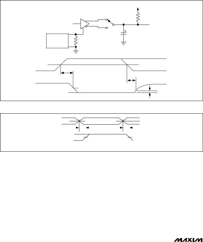
Figure 4a. Driver Enable and Disable Times (tDHZ, tDZH, tDZH(SHDN))
_______________________________________________________________________________________ 5
MAX13181E–MAX13184E
+5.0V, ±15kV ESD-Protected, Half-Duplex/ Full-Duplex, RS-485 Transceiver in µDFN
|
|
VCC |
|
|
RL = 500Ω |
|
|
S1 |
0 OR 3V |
D |
OUT |
|
DE |
CL |
|
|
50pF |
GENERATOR |
50Ω |
|
|
|
VCC |
DE |
|
VCC / 2 |
tDZL , tDZL(SHDN) |
|
0 |
|
|
|
|
|
tDLZ |
VCC |
|
VOH |
|
VOM = (VOL + VCC) / 2 |
|
OUT |
0.5V |
|
VOL |
|
|
|
|
Figure 4b. Driver Enable and Disable Times (tDLZ, tDZL, tDZL(SHDN))
A (Y) |
|
|
|
|
|
|
|
|
|
|
|
|
|
|
+1V |
B (Z) |
|
|
|
|
|
|
|
|
|
|
|
|
|
|
-1V |
|
|
|
|
|
|
|
tRPLH |
|
|
|
|
|
|
|
|
|
VOH |
|
|
|
|
|
|
|
|
|
|
|
|
||
|
|
|
|
|
|
|
|
|
|
tRPHL |
|||||
|
VOL |
|
1.5V |
|
|
|
|
|
|
|
|||||
RO |
|
|
|
|
|
|
|
|
|
|
|
|
|
||
|
|
|
|
|
tRSKEW |
= | tRPLH - tRPHL | |
|||||||||
|
|
|
|
|
|
||||||||||
THE RISE TIME AND FALL TIME OF INPUTS A, B, Y AND Z < 4ns
Figure 5. Receiver Propagation Delay
6_______________________________________________________________________________________
 Loading...