


Maxim MAX1247BMJE, MAX1247BEPE, MAX1247BEEE, MAX1247BCPE, MAX1247BCEE Datasheet
...KIT EVALUATION
AVAILABLE
Channel,
Serial 12-Bit ADCs in QSOP-16
Description
data-acquisition systems high-bandwidth with high conversion
. The MAX1246 oper-
.6V supply; the MAX1247 to +5.25V supply. Both configurable for
operation.
directly to SPI™/ without external logic. A connection to TMS320The MAX1246/MAX1247 external serial-interface analog-to-
2.5V reference, while the
. Both parts have with a ±1.5% voltage-
____________________________Features
♦4-Channel Single-Ended or 2-Channel Differential Inputs
♦Single-Supply Operation:
+2.7V to +3.6V (MAX1246)
+2.7V to +5.25V (MAX1247)
♦Internal 2.5V Reference (MAX1246)
♦Low Power: 1.2mA (133ksps, 3V supply)
54µA (1ksps, 3V supply) 1µA (power-down mode)
♦SPI/QSPI/Microwire/TMS320-Compatible 4-Wire Serial Interface
♦Software-Configurable Unipolar or Bipolar Inputs
♦16-Pin QSOP Package (same area as 8-pin SO)
-wired SHDN pin and a and can be prodown at the end of a coninterface automatically and the quick turn-on between all conversupply current to under
60µA at reduced sampling rates.
The MAX1246/MAX1247 are available in a 16-pin DIP and a small QSOP that occupies the same board area as an 8-pin SO.
For 8-channel versions of these devices, see the MAX146/MAX147 data sheet.
________________________Applications
Portable Data Logging |
Data Acquisition |
Medical Instruments |
Battery-Powered Instruments |
Pen Digitizers |
Process Control |
Pin Configuration appears at end of data sheet.
______________Ordering Information
PART† |
TEMP. RANGE |
PIN-PACKAGE |
INL |
|
|
|
(LSB) |
MAX1246ACPE |
0°C to +70°C |
16 Plastic DIP |
±1/2 |
|
|
|
|
MAX1246BCPE |
0°C to +70°C |
16 Plastic DIP |
±1 |
|
|
|
|
MAX1246ACEE |
0°C to +70°C |
16 QSOP |
±1/2 |
MAX1246BCEE |
0°C to +70°C |
16 QSOP |
±1 |
|
|
|
|
Ordering Information continued at end of data sheet.
†Contact factory for availability of alternate surface-mount packages.
__________Typical Operating Circuit
|
|
|
+3V |
|
CH0 |
VDD |
VDD |
0V TO |
|
DGND |
0.1μF |
|
|
||
+2.5V |
|
|
|
|
|
|
|
ANALOG |
MAX1246 AGND |
|
|
INPUTS |
CPU |
||
|
CH3 |
COM |
|
|
|
||
4.7μF |
VREF |
CS |
I/O |
|
SCLK |
SCK (SK) |
|
|
|
||
|
|
DIN |
MOSI (SO) |
0.047μF |
REFADJ |
DOUT |
MISO (SI) |
|
SSTRB |
|
|
|
|
VSS |
|
|
|
SHDN |
|
|
|
|
|
SPI and QSPI are registered trademarks of Motorola, Inc. Microwire is a registered trademark of National Semiconductor Corp.
________________________________________________________________ Maxim Integrated Products 1
For free samples & the latest literature: http://www.maxim-ic.com, or phone 1-800-998-8800
MAX1246/MAX1247

MAX1246/MAX1247
+2.7V, Low-Power, 4-Channel,
Serial 12-Bit ADCs in QSOP-16
ABSOLUTE MAXIMUM RATINGS
VDD to AGND, DGND................................................. |
|
- 0.3V to 6V |
AGND to DGND ...................................................... |
|
- 0.3V to 0.3V |
CH0–CH3, COM to AGND, DGND ............ |
-0.3V to (VDD + 0.3V) |
|
VREF to AGND........................................... |
-0.3V to (VDD + 0.3V) |
|
Digital Inputs to DGND .............................................. |
|
- 0.3V to 6V |
Digital Outputs to DGND ........................... |
-0.3V to (VDD + 0.3V) |
|
Digital Output Sink Current ................................................. |
|
25mA |
Continuous Power Dissipation (TA = +70°C) |
|
|
Plastic DIP (derate 10.53mW/°C above +70°C) |
......... 842mW |
|
QSOP (derate 8.36mW/°C above +70°C)................... |
667mW |
CERDIP (derate 10.00mW/°C above +70°C).............. |
800mW |
Operating Temperature Ranges |
|
MAX1246_C_E/MAX1247_C_E .......................... |
0°C to +70°C |
MAX1246_E_E/MAX1247_E_E........................ |
-40°C to +85°C |
MAX1246_MJE/MAX1247_MJE .................... |
-55°C to +125°C |
Storage Temperature Range ............................ |
-60°C to +150°C |
Lead Temperature (soldering, 10sec) ............................ |
+300°C |
Stresses beyond those listed under “Absolute Maximum Ratings” may cause permanent damage to the device. These are stress ratings only, and functional operation of the device at these or any other conditions beyond those indicated in the operational sections of the specifications is not implied. Exposure to absolute maximum rating conditions for extended periods may affect device reliability.
ELECTRICAL CHARACTERISTICS
(VDD = +2.7V to +3.6V (MAX1246); VDD = +2.7V to +5.25V (MAX1247); COM = 0V; fSCLK = 2.0MHz; external clock (50% duty cycle); 15 clocks/conversion cycle (133ksps); MAX1246—4.7µF capacitor at VREF pin; MAX1247—external reference, VREF = 2.500V applied to VREF pin; TA = TMIN to TMAX; unless otherwise noted.)
|
PARAMETER |
SYMBOL |
CONDITIONS |
MIN |
TYP |
MAX |
UNITS |
|
|
|
|
|
|
|
|
|
|
|
DC ACCURACY (Note 1) |
|
|
|
|
|
|
|
|
|
|
|
|
|
|
|
|
|
Resolution |
|
|
12 |
|
|
Bits |
|
|
|
|
|
|
|
|
|
|
|
Relative Accuracy (Note 2) |
INL |
MAX124_A |
|
|
±0.5 |
LSB |
|
|
|
|
|
|
|
|||
|
MAX124_B |
|
|
±1.0 |
|
|||
|
|
|
|
|
|
|
||
|
|
|
|
|
|
|
|
|
|
Differential Nonlinearity |
DNL |
No missing codes over temperature |
|
|
±1 |
LSB |
|
|
|
|
|
|
|
|
|
|
|
Offset Error |
|
MAX124_A |
|
±0.5 |
±3 |
LSB |
|
|
|
|
|
|
|
|
||
|
|
MAX124_B |
|
±0.5 |
±4 |
|
||
|
|
|
|
|||||
|
|
|
|
|
|
|||
|
|
|
|
|
|
|
|
|
|
Gain Error (Note 3) |
|
|
|
±0.5 |
±4 |
LSB |
|
|
|
|
|
|
|
|
|
|
|
Gain Temperature Coefficient |
|
|
|
±0.25 |
|
ppm/°C |
|
|
|
|
|
|
|
|
|
|
|
Channel-to-Channel Offset |
|
|
|
±0.25 |
|
LSB |
|
|
Matching |
|
|
|
|
|
||
|
|
|
|
|
|
|
|
|
|
|
|
|
|
|
|
|
|
DYNAMIC SPECIFICATIONS (10kHz sine-wave input, 0V to 2.500Vp-p, 133ksps, 2.0MHz external clock, bipolar input mode)
|
Signal-to-Noise + Distortion Ratio |
SINAD |
|
70 |
73 |
|
dB |
|
|
|
|
|
|
|
|
|
|
|
Total Harmonic Distortion |
THD |
Up to the 5th harmonic |
|
-88 |
-80 |
dB |
|
|
|
|
|
|
|
|
|
|
|
Spurious-Free Dynamic Range |
SFDR |
|
80 |
90 |
|
dB |
|
|
|
|
|
|
|
|
|
|
|
Channel-to-Channel Crosstalk |
|
65kHz, 2.500Vp-p (Note 4) |
|
-85 |
|
dB |
|
|
Small-Signal Bandwidth |
|
-3dB rolloff |
|
2.25 |
|
MHz |
|
|
|
|
|
|
|
|
|
|
|
Full-Power Bandwidth |
|
|
|
1.0 |
|
MHz |
|
|
|
|
|
|
|
|
|
|
|
CONVERSION RATE |
|
|
|
|
|
|
|
|
|
|
|
|
|
|
|
|
|
|
|
Internal clock, SHDN = FLOAT |
5.5 |
|
7.5 |
|
|
|
Conversion Time (Note 5) |
tCONV |
|
|
|
|
µs |
|
|
Internal clock, SHDN = VDD |
35 |
|
65 |
|
|||
|
|
|
External clock = 2MHz, 12 clocks/conversion |
6 |
|
|
|
|
|
|
|
|
|
|
|
|
|
|
Track/Hold Acquisition Time |
tACQ |
|
|
|
1.5 |
µs |
|
|
|
|
|
|
|
|
|
|
|
Aperture Delay |
|
|
|
30 |
|
ns |
|
|
|
|
|
|
|
|
|
|
|
Aperture Jitter |
|
|
|
<50 |
|
ps |
|
|
|
|
|
|
|
|
|
|
|
Internal Clock Frequency |
|
SHDN = FLOAT |
|
1.8 |
|
MHz |
|
|
|
|
|
|
|
|
||
|
|
SHDN = VDD |
|
0.225 |
|
|
||
|
|
|
|
|
|
|
||
|
External Clock Frequency |
|
|
0.1 |
|
2.0 |
MHz |
|
|
|
|
|
|
|
|
||
|
|
Data transfer only |
0 |
|
2.0 |
|
||
|
|
|
|
|
|
|||
|
|
|
|
|
|
|
|
|
2 _______________________________________________________________________________________

+2.7V, Low-Power, 4-Channel,
Serial 12-Bit ADCs in QSOP-16
ELECTRICAL CHARACTERISTICS (continued)
(VDD = +2.7V to +3.6V (MAX1246); VDD = +2.7V to +5.25V (MAX1247); COM = 0V; fSCLK = 2.0MHz; external clock (50% duty cycle); 15 clocks/conversion cycle (133ksps); MAX1246—4.7µF capacitor at VREF pin; MAX1247—external reference, VREF = 2.500V applied to VREF pin; TA = TMIN to TMAX; unless otherwise noted.)
PARAMETER |
SYMBOL |
CONDITIONS |
MIN |
TYP |
MAX |
UNITS |
|
|
|
|
|
|
|
ANALOG/COM INPUTS |
|
|
|
|
|
|
|
|
|
|
|
|
|
Input Voltage Range, Single- |
|
Unipolar, COM = 0V |
|
|
0 to VREF |
V |
|
|
|
|
|
||
Ended and Differential (Note 6) |
|
Bipolar, COM = VREF / 2 |
|
|
±VREF / 2 |
|
|
|
|
||||
|
|
|
|
|||
|
|
|
|
|
||
|
|
|
|
|
|
|
Multiplexer Leakage Current |
|
On/off leakage current, VCH_ = 0V or VDD |
|
±0.01 |
±1 |
µA |
Input Capacitance |
|
|
|
16 |
|
pF |
|
|
|
|
|
|
|
INTERNAL REFERENCE (MAX1246 only, reference buffer enabled) |
|
|
|
|
||
|
|
|
|
|
|
|
VREF Output Voltage |
|
TA = +25°C |
2.480 |
2.500 |
2.520 |
V |
VREF Short-Circuit Current |
|
|
|
|
30 |
mA |
|
|
|
|
|
|
|
|
|
MAX1246_C |
|
±30 |
±50 |
|
|
|
|
|
|||
|
|
|
|
|
|
|
VREF Temperature Coefficient |
|
MAX1246_E |
|
±30 |
±60 |
ppm/°C |
|
|
|||||
|
|
|
|
|
|
|
|
|
MAX1246_M |
|
±30 |
±80 |
|
|
|
|
|
|
|
|
Load Regulation (Note 8) |
|
0mA to 0.2mA output load |
|
±0.35 |
|
mV |
|
|
|
||||
|
|
|
|
|
|
|
Capacitive Bypass at VREF |
|
Internal compensation mode |
0 |
|
|
µF |
|
|
|
||||
|
|
|
|
|
||
|
External compensation mode |
4.7 |
|
|
||
|
|
|
|
|
||
|
|
|
|
|
|
|
Capacitive Bypass at REFADJ |
|
|
0.047 |
|
|
µF |
|
|
|
|
|||
|
|
|
|
|
|
|
REFADJ Adjustment Range |
|
|
|
±1.5 |
|
% |
|
|
|
|
|||
|
|
|
|
|
|
|
EXTERNAL REFERENCE AT VREF (Buffer |
disabled) |
|
|
|
|
|
|
|
|
|
|
|
|
VREF Input Voltage Range |
|
|
1.0 |
|
VDD + |
V |
(Note 9) |
|
|
|
50mV |
||
|
|
|
|
|
||
|
|
|
|
|
|
|
VREF Input Current |
|
VREF = 2.500V |
|
100 |
150 |
µA |
|
|
|
|
|
|
|
VREF Input Resistance |
|
|
18 |
25 |
|
kΩ |
|
|
|
|
|
|
|
Shutdown VREF Input Current |
|
|
|
0.01 |
10 |
µA |
|
|
|
|
|
|
|
REFADJ Buffer Disable Threshold |
|
|
VDD - |
|
|
V |
|
|
|
|
|||
|
|
0.5 |
|
|
||
|
|
|
|
|
|
|
|
|
|
|
|
|
|
EXTERNAL REFERENCE AT REFADJ |
|
|
|
|
|
|
|
|
|
|
|
|
|
Capacitive Bypass at VREF |
|
Internal compensation mode |
0 |
|
|
µF |
|
|
|
|
|
||
|
External compensation mode |
4.7 |
|
|
||
|
|
|
|
|
||
|
|
|
|
|
|
|
Reference Buffer Gain |
|
MAX1246 |
|
2.06 |
|
V/V |
|
|
|
||||
|
|
|
|
|
||
|
MAX1247 |
|
2.00 |
|
||
|
|
|
|
|
||
|
|
|
|
|
|
|
REFADJ Input Current |
|
MAX1246 |
|
|
±50 |
µA |
|
|
|
|
|
||
|
MAX1247 |
|
|
±10 |
||
|
|
|
|
|
||
|
|
|
|
|
|
|
MAX1246/MAX1247
_______________________________________________________________________________________ 3

MAX1246/MAX1247
+2.7V, Low-Power, 4-Channel,
Serial 12-Bit ADCs in QSOP-16
ELECTRICAL CHARACTERISTICS (continued)
(VDD = +2.7V to +3.6V (MAX1246); VDD = +2.7V to +5.25V (MAX1247); COM = 0V; fSCLK = 2.0MHz; external clock (50% duty cycle); 15 clocks/conversion cycle (133ksps); MAX1246—4.7µF capacitor at VREF pin; MAX1247—external reference, VREF = 2.500V applied to VREF pin; TA = TMIN to TMAX; unless otherwise noted.)
PARAMETER |
SYMBOL |
|
|
|
|
CONDITIONS |
MIN |
TYP |
MAX |
UNITS |
||||
|
|
|
|
|
|
|
|
|
|
|
|
|
|
|
DIGITAL INPUTS (DIN, SCLK, |
|
|
|
|
|
|
|
|
|
|
|
|
|
|
CS, |
SHDN) |
|
|
|
|
|
|
|
|
|
|
|||
|
|
|
|
|
|
|
|
|
|
|
|
|
|
|
DIN, SCLK, CS Input High Voltage |
|
VIH |
|
|
VDD ≤ 3.6V |
|
2.0 |
|
|
V |
||||
|
|
|
VDD > 3.6V, MAX1247 only |
3.0 |
|
|
||||||||
|
|
|
|
|
|
|
|
|
|
|||||
DIN, SCLK, CS Input Low Voltage |
|
VIL |
|
|
|
|
|
|
|
|
0.8 |
V |
||
|
|
|
|
|
|
|
|
|
|
|
|
|
|
|
DIN, SCLK, CS Input Hysteresis |
|
VHYST |
|
|
|
|
|
|
|
0.2 |
|
V |
||
|
|
|
|
|
|
|
|
|
|
|
|
|
|
|
DIN, SCLK, CS Input Leakage |
|
IIN |
|
|
VIN = 0V or VDD |
|
|
±0.01 |
±1 |
µA |
||||
DIN, SCLK, CS Input Capacitance |
|
CIN |
|
|
(Note 7) |
|
|
|
15 |
pF |
||||
|
|
|
|
|
|
|
|
|
|
|
|
|
|
|
SHDN Input High Voltage |
|
VSH |
|
|
|
|
|
|
VDD - 0.4 |
|
|
V |
||
SHDN Input Mid Voltage |
|
VSM |
|
|
|
|
|
|
1.1 |
|
VDD - 1.1 |
V |
||
SHDN Input Low Voltage |
|
VSL |
|
|
|
|
|
|
|
|
0.4 |
V |
||
|
|
|
|
|
|
|
|
|
|
|
|
|
|
|
SHDN Input Current |
|
IS |
|
|
|
= 0V or VDD |
|
|
|
±4.0 |
µA |
|||
|
|
SHDN |
|
|
|
|||||||||
SHDN Voltage, Floating |
|
VFLT |
|
|
SHDN |
= FLOAT |
|
|
VDD / 2 |
|
V |
|||
SHDN Maximum Allowed |
|
|
|
|
|
|
|
|
|
|
|
|
|
|
|
|
|
|
|
SHDN = FLOAT |
|
|
|
±100 |
nA |
||||
Leakage, Mid Input |
|
|
|
|
|
|
|
|
||||||
|
|
|
|
|
|
|
|
|
|
|
|
|
||
|
|
|
|
|
|
|
|
|
|
|
|
|
|
|
DIGITAL OUTPUTS (DOUT, SSTRB) |
|
|
|
|
|
|
|
|
|
|
||||
|
|
|
|
|
|
|
|
|
|
|
|
|
|
|
Output Voltage Low |
|
VOL |
|
|
ISINK = 5mA |
|
|
|
0.4 |
V |
||||
|
|
|
ISINK = 16mA |
|
|
|
0.8 |
|||||||
|
|
|
|
|
|
|
|
|
|
|
||||
Output Voltage High |
|
VOH |
|
|
ISOURCE = 0.5mA |
|
VDD - 0.5 |
|
|
V |
||||
Three-State Leakage Current |
|
IL |
|
|
CS = VDD |
|
|
±0.01 |
±10 |
µA |
||||
Three-State Output Capacitance |
|
COUT |
|
|
CS = VDD (Note 7) |
|
|
|
15 |
pF |
||||
POWER REQUIREMENTS |
|
|
|
|
|
|
|
|
|
|
|
|
|
|
|
|
|
|
|
|
|
|
|
|
|
|
|
|
|
Positive Supply Voltage |
|
VDD |
|
|
MAX1246 |
|
2.70 |
|
3.60 |
V |
||||
|
|
|
|
|
|
|
|
|
|
|||||
|
MAX1247 |
|
2.70 |
|
5.25 |
|||||||||
|
|
|
||||||||||||
|
|
|
|
|
|
|
|
|
|
|||||
|
|
|
|
|
|
|
|
|
|
|
|
|
|
|
|
|
|
|
|
|
|
|
|
Operating mode, full-scale input |
|
1.2 |
2.0 |
mA |
|
|
|
|
|
|
|
|
|
|
|
|
|
|
|
|
Positive Supply Current, MAX1246 |
|
IDD |
|
|
VDD = 3.6V |
Fast power-down |
|
30 |
70 |
µA |
||||
|
|
|
|
|
|
|
|
|
|
|
|
|
|
|
|
|
|
|
|
|
|
|
|
Full power-down |
|
1.2 |
10 |
||
|
|
|
|
|
|
|
|
|
|
|
||||
|
|
|
|
|
|
|
|
|
|
|
|
|
|
|
|
|
|
|
|
|
|
Operating mode, |
VDD = 5.25V |
|
1.8 |
2.5 |
mA |
||
|
|
|
|
|
|
|
full-scale input |
|
|
|
|
|||
|
|
|
|
|
|
|
VDD = 3.6V |
|
0.9 |
1.5 |
||||
|
|
|
|
|
|
|
|
|
||||||
|
|
|
|
|
|
|
|
|
|
|
|
|
|
|
Positive Supply Current, MAX1247 |
|
IDD |
|
|
Fast power-down |
|
|
30 |
70 |
|
||||
|
|
|
|
|
|
|||||||||
|
|
|
|
|
|
|
|
|
|
|
|
|
|
|
|
|
|
|
|
|
|
Full power-down |
VDD = 5.25V |
|
3.5 |
15 |
µA |
||
|
|
|
|
|
|
|
|
|
|
|
|
|||
|
|
|
|
|
|
|
VDD = 3.6V |
|
1.2 |
10 |
|
|||
|
|
|
|
|
|
|
|
|
|
|
|
|||
|
|
|
|
|
|
|
|
|
|
|
|
|
|
|
Supply Rejection (Note 10) |
|
PSR |
|
VDD = 2.7V to VDD(MAX), full-scale input, |
|
±0.3 |
|
mV |
||||||
|
|
external reference = 2.500V |
|
|
||||||||||
|
|
|
|
|
|
|
|
|
|
|
||||
|
|
|
|
|
|
|
|
|
|
|
|
|
|
|
4 _______________________________________________________________________________________
+2.7V, Low-Power, 4-Channel,
Serial 12-Bit ADCs in QSOP-16
TIMING CHARACTERISTICS
(VDD = +2.7V to +3.6V (MAX1246); VDD = +2.7V to +5.25V (MAX1247); TA = TMIN to TMAX; unless otherwise noted.)
PARAMETER |
|
SYMBOL |
|
CONDITIONS |
|
MIN |
TYP |
MAX |
UNITS |
|
|
|
|
|
|
|
|
|
|
Acquisition Time |
|
tACQ |
|
|
|
1.5 |
|
|
µs |
|
|
|
|
|
|
|
|
|
|
DIN to SCLK Setup |
tDS |
|
|
|
100 |
|
|
ns |
|
|
|
|
|
|
|
|
|
|
|
DIN to SCLK Hold |
|
tDH |
|
|
|
|
|
0 |
ns |
|
|
|
|
|
|
|
|
|
|
SCLK Fall to Output Data Valid |
|
tDO |
Figure 1 |
MAX124_ _C/E |
|
20 |
|
200 |
ns |
|
|
|
|
|
|
||||
MAX124Figure _ _M |
|
20 |
|
240 |
|||||
|
|
|
|
|
|
|
|||
|
|
|
|
|
|
|
|
|
|
CS Fall to Output Enable |
|
tDV |
Figure 1 |
|
|
|
240 |
ns |
|
|
|
|
|
|
|
|
|
|
|
CS Rise to Output Disable |
|
tTR |
Figure 2 |
|
|
|
240 |
ns |
|
|
|
|
|
|
|
|
|
|
|
CS to SCLK Rise Setup |
|
tCSS |
|
|
|
100 |
|
|
ns |
|
|
|
|
|
|
|
|
|
|
CS to SCLK Rise Hold |
|
tCSH |
|
|
|
0 |
|
|
ns |
|
|
|
|
|
|
|
|
|
|
SCLK Pulse Width High |
|
tCH |
|
|
|
200 |
|
|
ns |
|
|
|
|
|
|
|
|
|
|
SCLK Pulse Width Low |
|
tCL |
|
|
|
200 |
|
|
ns |
|
|
|
|
|
|
|
|
|
|
SCLK Fall to SSTRB |
|
tSSTRB |
Figure 1 |
|
|
|
240 |
ns |
|
|
|
|
|
|
|
|
|
|
|
CS Fall to SSTRB Output Enable |
|
tSDV |
External clock mode only, Figure 1 |
|
|
|
240 |
ns |
|
|
|
|
|
|
|
|
|
|
|
CS Rise to SSTRB Output Disable |
|
tSTR |
External clock mode only, Figure 2 |
|
|
|
240 |
ns |
|
|
|
|
|
|
|
|
|
|
|
SSTRB Rise to SCLK Rise |
|
tSCK |
Internal clock mode only (Note 7) |
0 |
|
|
ns |
||
|
|
|
|
|
|
|
|
|
|
Note 1: Tested at VDD = 2.7V; COM = 0V; unipolar single-ended input mode.
Note 2: Relative accuracy is the deviation of the analog value at any code from its theoretical value after the full-scale range has been calibrated.
Note 3: MAX1246—internal reference, offset nulled; MAX1247—external reference (VREF = +2.500V), offset nulled. Note 4: Ground “on” channel; sine wave applied to all “off” channels.
Note 5: Conversion time defined as the number of clock cycles multiplied by the clock period; clock has 50% duty cycle. Note 6: The common-mode range for the analog inputs is from AGND to VDD.
Note 7: Guaranteed by design. Not subject to production testing.
Note 8: External load should not change during conversion for specified accuracy. Note 9: ADC performance is limited by the converter’s noise floor, typically 300µVp-p. Note 10: Measured as |VFS(2.7V) - VFS(VDD, MAX)|.
__________________________________________Typical Operating Characteristics
(VDD = 3.0V, VREF = 2.500V, fSCLK = 2.0MHz, CLOAD = 20pF, TA = +25°C, unless otherwise noted.)
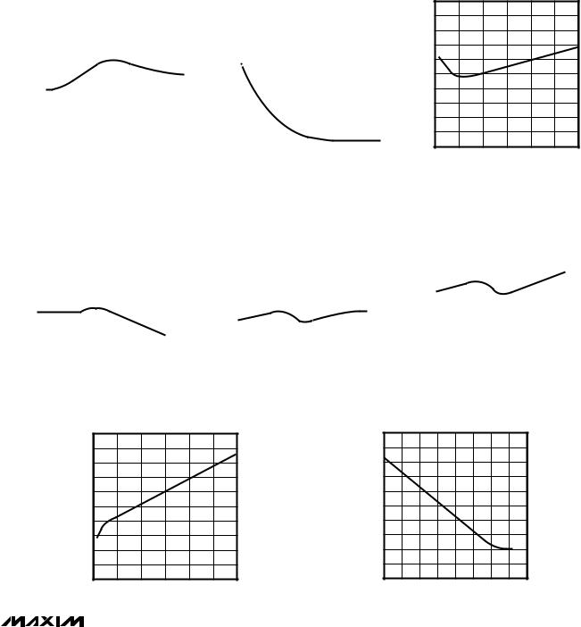
INTEGRAL NONLINEARITY |
INTEGRAL NONLINEARITY |
INTEGRAL NONLINEARITY |
vs. CODE |
vs. SUPPLY VOLTAGE |
vs. TEMPERATURE |
|
0.5 |
|
|
|
MAX1247-01 |
|
0.50 |
|
|
|
|
|
MAX1247-02 |
|
0.50 |
|
VDD = 2.7V |
|
|
|
MAX1247-03 |
|
0.4 |
|
|
|
|
0.45 |
|
|
|
|
|
|
0.45 |
|
|
|
|
||||
|
0.3 |
|
|
|
|
|
0.40 |
|
|
MAX1246 |
|
|
|
|
0.40 |
|
|
|
|
|
|
|
0.2 |
|
|
|
|
|
0.35 |
|
|
|
|
|
|
0.35 |
|
|
|
|
|
|
|
|
|
|
|
|
|
|
|
|
|
|
|
|
|
|
|
|
|
|
|||
(LSB) |
0.1 |
|
|
|
|
(LSB) |
0.30 |
|
|
|
|
|
|
(LSB) |
0.30 |
|
MAX1246 |
|
|
|
|
0 |
|
|
|
|
0.25 |
|
|
|
|
|
|
0.25 |
|
|
|
|
|
|
|||
INL |
|
|
|
|
INL |
|
|
|
|
|
|
INL |
|
|
|
|
|
|
|||
-0.1 |
|
|
|
|
0.20 |
|
|
|
|
|
|
0.20 |
|
|
|
|
|
|
|||
|
|
|
|
|
|
|
|
MAX1247 |
|
|
|
|
|
|
|
MAX1247 |
|
||||
|
-0.2 |
|
|
|
|
|
0.15 |
|
|
|
|
|
|
0.15 |
|
|
|
|
|||
|
|
|
|
|
|
|
|
|
|
|
|
|
|
|
|
|
|
|
|||
|
-0.3 |
|
|
|
|
|
0.10 |
|
|
|
|
|
|
|
0.10 |
|
|
|
|
|
|
|
-0.4 |
|
|
|
|
|
0.05 |
|
|
|
|
|
|
|
0.05 |
|
|
|
|
|
|
|
-0.5 |
|
|
|
|
|
0.00 |
|
|
|
|
|
|
|
0.00 |
-60 |
-20 |
20 |
60 |
100 |
140 |
|
0 |
1024 |
2048 |
3072 |
4096 |
|
2.25 |
2.75 |
3.25 |
3.75 |
4.25 |
4.75 |
5.25 |
|
|
||||||
|
|
|
CODE |
|
|
|
|
|
|
VDD (V) |
|
|
|
|
|
|
|
TEMPERATURE (°C) |
|
|
|
|
|
|
_______________________________________________________________________________________ |
5 |
|||||||||||||||||
MAX1246/MAX1247

+2.7V, Low-Power, 4-Channel,
Serial 12-Bit ADCs in QSOP-16
MAX1246/MAX1247 |
____________________________Typical Operating Characteristics (continued) |
|||||||||||||||||||||
(VDD = 3.0V, VREF = 2.500V, fSCLK = 2.0MHz, CLOAD = 20pF, TA = +25°C, unless otherwise noted.) |
|
|
|
|
|
|||||||||||||||||
|
|
|
SUPPLY CURRENT |
|
|
|
|
SHUTDOWN SUPPLY CURRENT |
|
|
|
INTERNAL REFERENCE VOLTAGE |
|
|||||||||
|
2.00 |
|
vs. SUPPLY VOLTAGE |
|
|
|
4.0 |
vs. SUPPLY VOLTAGE |
|
|
|
|
vs. SUPPLY VOLTAGE |
|
|
|||||||
|
RL = ∞ |
|
|
|
04 |
|
|
|
|
|
05 |
|
2.5020 |
|
|
|
|
5.25MAX1247-06 |
||||
|
|
|
|
|
- |
|
|
|
FULL POWER-DOWN |
- |
|
|
|
|
|
|
||||||
|
|
|
CLOAD = 50pF |
MAX1247 |
|
3.5 |
|
MAX1247 |
|
|
|
|
|
|
||||||||
|
1.75 |
CODE = 101010100000 |
SHUTDOWN SUPPLY CURRENT (μA) |
|
|
|
|
|
2.5015 |
|
|
|
|
|||||||||
|
|
|
|
|
|
|
|
|
|
|
|
|
|
|
|
|
|
|||||
SUPPLY CURRENT (mA) |
|
|
|
|
|
|
|
3.0 |
|
|
|
|
|
|
|
|
|
|
|
|||
1.50 |
MAX1246 |
|
|
|
|
2.5 |
|
|
|
|
|
|
2.5010 |
|
|
|
|
|||||
|
|
|
|
|
|
|
|
|
|
VREF (V) |
|
|
|
|
|
|||||||
1.25 |
|
|
|
|
|
|
2.0 |
|
|
|
|
|
2.5005 |
|
|
|
|
|||||
1.00 |
|
|
|
|
|
|
1.5 |
|
|
|
|
|
2.5000 |
|
|
|
|
|||||
|
|
|
CLOAD |
= 20pF |
|
|
|
|
|
|
|
|
|
|
|
|||||||
|
|
|
|
|
1.0 |
|
|
|
|
|
|
|
|
|
|
|||||||
|
|
|
|
|
|
|
|
|
|
|
|
|
|
|
|
|
||||||
0.75 |
|
MAX1247 |
|
|
|
|
0.5 |
|
|
|
|
|
2.4995 |
|
|
|
|
|||||
|
|
|
|
|
|
|
|
|
|
|
|
|
|
|
|
|||||||
0.50 |
|
|
|
|
|
|
0 |
|
|
|
|
|
2.4990 |
|
|
|
|
|||||
2.25 |
2.75 3.25 |
3.75 |
4.25 |
4.75 |
5.25 |
2.25 |
2.75 3.25 |
3.75 |
4.25 |
4.75 |
5.25 |
2.25 |
2.75 3.25 |
3.75 |
4.25 |
4.75 |
||||||
SUPPLY VOLTAGE (V) |
VDD (V) |
VDD (V) |
SUPPLY CURRENT (mA)
SUPPLY CURRENT vs. TEMPERATURE
1.3 |
|
|
|
|
|
|
|
|
|
07 |
|||
|
|
|
|
|
|
MAX1247- |
1.2 |
|
MAX1246 |
|
|||
|
|
|
|
|
|
|
|
|
|
|
|
|
|
1.1
1.0
MAX1247
0.9
RLOAD = ∞
CODE = 101010100000
0.8
-60 |
-20 |
20 |
60 |
100 |
140 |
|
|
TEMPERATURE (°C) |
|
|
|
SHUTDOWN CURRENT (μA)
SHUTDOWN CURRENT vs. TEMPERATURE
2.0
MAX1247-08
1.6
1.2
0.8
0.4
0
-60 |
-20 |
20 |
60 |
100 |
140 |
TEMPERATURE (°C)
VREF (V)
2.501
2.500
2.499
2.498
2.497
2.496
2.495
2.494
-60
MAX1246
INTERNAL REFERENCE VOLTAGE vs. TEMPERATURE
MAX1247-09
VDD = 3.6V
VDD = 2.7V
-20 |
20 |
60 |
100 |
140 |
|
TEMPERATURE (°C) |
|
|
|
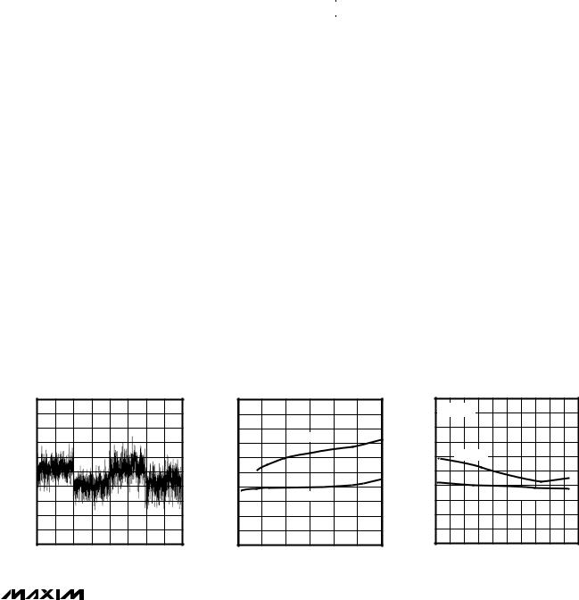
AMPLITUDE (dB)
|
|
|
|
|
|
FFT PLOT |
|
|
|
|
|
|
|
|||
20 |
|
|
|
|
|
|
|
|
|
|
|
|
|
|
|
-10 |
|
|
|
|
|
|
|
|
|
|
VDD = 2.7V |
|
|
MAX1247 |
|||
0 |
|
|
|
|
|
|
|
|
|
fIN = 10k |
|
|
|
|
||
|
|
|
|
|
|
|
|
|
|
|
|
|
|
|||
|
|
|
|
|
|
|
|
|
|
|
|
|
|
|||
|
|
|
|
|
|
|
|
|
|
fSAMPLE = 133k |
|
|
|
|||
-20 |
|
|
|
|
|
|
|
|
|
|
|
|
|
|
|
|
|
|
|
|
|
|
|
|
|
|
|
|
|
|
|
|
|
-40 |
|
|
|
|
|
|
|
|
|
|
|
|
|
|
|
|
|
|
|
|
|
|
|
|
|
|
|
|
|
|
|
|
|
-60 |
|
|
|
|
|
|
|
|
|
|
|
|
|
|
|
|
|
|
|
|
|
|
|
|
|
|
|
|
|
|
|
|
|
-80 |
|
|
|
|
|
|
|
|
|
|
|
|
|
|
|
|
|
|
|
|
|
|
|
|
|
|
|
|
|
|
|
|
|
-100 |
|
|
|
|
|
|
|
|
|
|
|
|
|
|
|
|
|
|
|
|
|
|
|
|
|
|
|
|
|
|
|
|
|
-120 |
|
|
|
|
|
|
|
|
|
|
|
|
|
|
|
|
|
|
|
|
|
|
|
|
|
|
|
|
|
|
|
|
|
0 |
10 |
20 |
30 |
40 |
50 |
60 |
70 |
|||||||||
|
|
|
|
|
|
FREQUENCY (kHz) |
|
|
|
|
|
|||||
EFFECTIVE NUMBER OF BITS
EFFECTIVE NUMBER OF BITS vs. FREQUENCY
12.0 |
|
|
|
|
|
-11 |
|
|
|
|
|
||
|
|
VDD = 2.7V |
|
MAX1247 |
||
11.8
11.6
11.4
11.2
11.0
1 |
10 |
100 |
FREQUENCY (kHz)
6 _______________________________________________________________________________________
+2.7V, Low-Power, 4-Channel,
Serial 12-Bit ADCs in QSOP-16
____________________________Typical Operating Characteristics (continued)
(VDD = 3.0V, VREF = 2.500V, fSCLK = 2.0MHz, CLOAD = 20pF, TA = +25°C, unless otherwise noted.)
|
GAIN ERROR |
CHANNEL-TO-CHANNEL GAIN MATCHING |
OFFSET vs. SUPPLY VOLTAGE |
vs. SUPPLY VOLTAGE |
vs. SUPPLY VOLTAGE |
OFFSET (LSB)
0.50 |
|
|
|
|
|
|
|
|
|
|
|
|
-12 |
|
|
|
|
|
|
|
|
|
|
|
|
||
0.45 |
|
|
|
|
|
|
|
|
|
|
|
|
MAX1247 |
|
|
|
|
|
|
|
|
|
|
|
|
||
0.40 |
|
|
|
|
|
|
|
|
|
|
|
|
|
|
|
|
|
|
|
|
|
|
|
|
|
|
|
0.35 |
|
|
|
|
|
|
|
|
|
|
|
|
|
|
|
|
|
|
|
|
|
|
|
|
|
|
|
0.30 |
|
|
|
|
|
|
|
|
|
|
|
|
|
|
|
|
|
|
|
|
|
|
|
|
|
|
|
0.25 |
|
|
|
|
|
|
|
|
|
|
|
|
|
|
|
|
|
|
|
|
|
|
|
|
|
|
|
0.20 |
|
|
|
|
|
|
|
|
|
|
|
|
|
|
|
|
|
|
|
|
|
|
|
|
|
|
|
0.15 |
|
|
|
|
|
|
|
|
|
|
|
|
|
|
|
|
|
|
|
|
|
|
|
|
|
|
|
0.10 |
|
|
|
|
|
|
|
|
|
|
|
|
|
|
|
|
|
|
|
|
|
|
|
|
|
|
|
0.05 |
|
|
|
|
|
|
|
|
|
|
|
|
|
|
|
|
|
|
|
|
|
|
|
|
|
|
|
0 |
|
|
|
|
|
|
|
|
|
|
|
|
|
|
|
|
|
|
|
|
|
|
|
|
|
|
|
2.25 |
2.75 |
3.25 |
3.75 |
4.25 |
4.75 |
5.25 |
|||||||
GAIN ERROR (LSB)
0.50 |
|
|
|
|
|
|
|
|
|
|
|
|
-13 |
|
|
|
|
|
|
|
|
|
|
|
|
||
0.45 |
|
|
|
|
|
|
|
|
|
|
|
|
MAX1247 |
|
|
|
|
|
|
|
|
|
|
|
|
||
0.40 |
|
|
|
|
|
|
|
|
|
|
|
|
|
|
|
|
|
|
|
|
|
|
|
|
|
|
|
0.35 |
|
|
|
|
|
|
|
|
|
|
|
|
|
|
|
|
|
|
|
|
|
|
|
|
|
|
|
0.30 |
|
|
|
|
|
|
|
|
|
|
|
|
|
|
|
|
|
|
|
|
|
|
|
|
|
|
|
0.25 |
|
|
|
|
|
|
|
|
|
|
|
|
|
|
|
|
|
|
|
|
|
|
|
|
|
|
|
0.20 |
|
|
|
|
|
|
|
|
|
|
|
|
|
|
|
|
|
|
|
|
|
|
|
|
|
|
|
0.15 |
|
|
|
|
|
|
|
|
|
|
|
|
|
|
|
|
|
|
|
|
|
|
|
|
|
|
|
0.10 |
|
|
|
|
|
|
|
|
|
|
|
|
|
|
|
|
|
|
|
|
|
|
|
|
|
|
|
0.05 |
|
|
|
|
|
|
|
|
|
|
|
|
|
|
|
|
|
|
|
|
|
|
|
|
|
|
|
0 |
|
|
|
|
|
|
|
|
|
|
|
|
|
|
2.75 |
3.25 |
3.75 |
4.25 |
4.75 |
5.25 |
|||||||
2.25 |
|||||||||||||
|
0.50 |
|
|
|
|
|
-14 |
|
0.45 |
|
|
|
|
|
MAX1247 |
(LSB) |
0.40 |
|
|
|
|
|
|
0.35 |
|
|
|
|
|
|
|
|
|
|
|
|
|
|
|
MATCHING |
0.30 |
|
|
|
|
|
|
0.25 |
|
|
|
|
|
|
|
0.20 |
|
|
|
|
|
|
|
GAIN |
|
|
|
|
|
|
|
0.15 |
|
|
|
|
|
|
|
|
|
|
|
|
|
|
|
|
0.10 |
|
|
|
|
|
|
|
0.05 |
|
|
|
|
|
|
|
0 |
|
|
|
|
|
|
|
2.25 |
2.75 |
3.25 |
3.75 |
4.25 |
4.75 |
5.25 |
VDD (V) VDD (V) VDD (V)
|
|
|
|
|
|
|
|
|
|
|
|
|
|
|
|
GAIN ERROR |
|
|
|
|
CHANNEL-TO-CHANNEL GAIN MATCHING |
||||||||||||||
|
|
|
OFFSET vs. TEMPERATURE |
|
|
|
|
|
|
vs. TEMPERATURE |
|
|
|
|
|
|
|
vs. TEMPERATURE |
|
|
|
||||||||||||||
|
0.50 |
|
|
|
|
|
|
|
|
|
MAX1247-15 |
|
0.50 |
|
|
|
|
|
|
|
|
|
MAX1247-16 |
|
0.50 |
|
|
|
|
|
|
|
|
|
MAX1247-17 |
|
0.45 |
|
|
|
|
|
|
|
|
|
|
0.45 |
|
|
|
|
|
|
|
|
|
|
0.45 |
|
|
|
|
|
|
|
|
|
|||
|
|
|
|
|
|
|
|
|
|
|
|
|
|
|
|
|
|
|
|
|
|
|
|
|
|
|
|
|
|
||||||
(LSB)OFFSET |
0.40 |
|
|
|
|
|
|
|
|
|
|
(LSB)ERRORGAIN |
0.40 |
|
|
|
|
|
|
|
|
|
|
(LSB)MATCHINGGAIN |
0.40 |
|
|
|
|
|
|
|
|
|
|
|
|
|
|
|
|
|
|
|
|
|
|
|
|
|
|
|
|
|
|
|
|
|
|
|
|
|
|
|
|
||||||
0.35 |
|
|
|
|
|
|
|
|
|
|
0.35 |
|
|
|
|
|
|
|
|
|
|
0.35 |
|
|
|
|
|
|
|
|
|
|
|||
|
|
|
|
|
|
|
|
|
|
|
|
|
|
|
|
|
|
|
|
|
|
|
|
|
|
|
|
|
|
|
|
|
|||
|
0.30 |
|
|
|
|
|
|
|
|
|
|
|
0.30 |
|
|
|
|
|
|
|
|
|
|
|
0.30 |
|
|
|
|
|
|
|
|
|
|
|
|
|
|
|
|
|
|
|
|
|
|
|
|
|
|
|
|
|
|
|
|
|
|
|
|
|
|
|
|
|
|
|
|||
|
0.25 |
|
|
|
|
|
|
|
|
|
|
|
0.25 |
|
|
|
|
|
|
|
|
|
|
|
0.25 |
|
|
|
|
|
|
|
|
|
|
|
|
|
|
|
|
|
|
|
|
|
|
|
|
|
|
|
|
|
|
|
|
|
|
|
|
|
|
|
|
|
|
|
|||
|
0.20 |
|
|
|
|
|
|
|
|
|
|
|
0.20 |
|
|
|
|
|
|
|
|
|
|
|
0.20 |
|
|
|
|
|
|
|
|
|
|
|
|
|
|
|
|
|
|
|
|
|
|
|
|
|
|
|
|
|
|
|
|
|
|
|
|
|
|
|
|
|
|
|
|||
|
0.15 |
|
|
|
|
|
|
|
|
|
|
|
0.15 |
|
|
|
|
|
|
|
|
|
|
|
0.15 |
|
|
|
|
|
|
|
|
|
|
|
|
|
|
|
|
|
|
|
|
|
|
|
|
|
|
|
|
|
|
|
|
|
|
|
|
|
|
|
|
|
|
|
|||
|
0.10 |
|
|
|
|
|
|
|
|
|
|
|
0.10 |
|
|
|
|
|
|
|
|
|
|
|
0.10 |
|
|
|
|
|
|
|
|
|
|
|
|
|
|
|
|
|
|
|
|
|
|
|
|
|
|
|
|
|
|
|
|
|
|
|
|
|
|
|
|
|
|
|
|||
|
0.05 |
|
|
|
|
|
|
|
|
|
|
|
0.05 |
|
|
|
|
|
|
|
|
|
|
|
0.05 |
|
|
|
|
|
|
|
|
|
|
|
|
|
|
|
|
|
|
|
|
|
|
|
|
|
|
|
|
|
|
|
|
|
|
|
|
|
|
|
|
|
|
|
|||
|
0 |
|
|
|
|
|
|
|
|
|
|
|
0 |
|
|
|
|
|
|
|
|
|
|
|
0 |
|
|
|
|
|
|
|
|
|
|
|
-55 -30 -5 20 45 70 95 120 |
145 |
|
-55 -30 -5 20 45 70 95 |
120 145 |
|
-55 -30 -5 20 45 70 95 |
120 145 |
|||||||||||||||||||||||||||
|
|
|
|
TEMPERATURE (˚C) |
|
|
|
|
|
|
TEMPERATURE (˚C) |
|
|
|
|
|
|
|
TEMPERATURE (˚C) |
|
|
|
|||||||||||||
CHANNEL-TO-CHANNEL OFFSET MATCHING vs. SUPPLY VOLTAGE
|
0.50 |
|
|
|
|
|
-18 |
|
0.45 |
|
|
|
|
|
MAX1247 |
(LSB) |
0.40 |
|
|
|
|
|
|
0.35 |
|
|
|
|
|
|
|
MATCHING |
0.30 |
|
|
|
|
|
|
0.25 |
|
|
|
|
|
|
|
0.20 |
|
|
|
|
|
|
|
OFFSET |
|
|
|
|
|
|
|
0.15 |
|
|
|
|
|
|
|
|
0.10 |
|
|
|
|
|
|
|
0.05 |
|
|
|
|
|
|
|
0 |
2.75 |
3.25 |
3.75 |
4.25 |
4.75 |
5.25 |
|
2.25 |
VDD (V)
CHANNEL-TO-CHANNEL OFFSET MATCHING vs. TEMPERATURE
|
0.50 |
|
|
|
|
|
|
|
-19 |
|
0.45 |
|
|
|
|
|
|
|
MAX1247 |
(LSB) |
0.40 |
|
|
|
|
|
|
|
|
0.35 |
|
|
|
|
|
|
|
|
|
MATCHING |
0.30 |
|
|
|
|
|
|
|
|
0.25 |
|
|
|
|
|
|
|
|
|
0.20 |
|
|
|
|
|
|
|
|
|
OFFSET |
|
|
|
|
|
|
|
|
|
0.15 |
|
|
|
|
|
|
|
|
|
|
|
|
|
|
|
|
|
|
|
|
0.10 |
|
|
|
|
|
|
|
|
|
0.05 |
|
|
|
|
|
|
|
|
|
0 |
-30 |
-5 |
|
|
|
|
|
|
|
-55 |
20 |
45 |
70 |
95 |
120 |
145 |
TEMPERATURE (˚C)
MAX1246/MAX1247
_______________________________________________________________________________________ 7
MAX1246/MAX1247
+2.7V, Low-Power, 4-Channel,
Serial 12-Bit ADCs in QSOP-16
______________________________________________________________Pin Description
PIN |
NAME |
FUNCTION |
|
|
|
|
|
1 |
VDD |
Positive Supply Voltage |
|
|
|
|
|
2–5 |
CH0–CH3 |
Sampling Analog Inputs |
|
|
|
|
|
6 |
COM |
Ground reference for analog inputs. COM sets zero-code voltage in single-ended mode. Must be |
|
stable to ±0.5LSB. |
|||
|
|
||
|
|
|
|
|
|
Three-Level Shutdown Input. Pulling SHDN low shuts the MAX1246/MAX1247 down; otherwise, they |
|
7 |
SHDN |
are fully operational. Pulling SHDN high puts the reference-buffer amplifier in internal compensation |
|
|
|
mode. Letting SHDN float puts the reference-buffer amplifier in external compensation mode. |
|
|
|
|
|
|
|
Reference-Buffer Output/ADC Reference Input. Reference voltage for analog-to-digital conversion. |
|
8 |
VREF |
In internal reference mode (MAX1246 only), the reference buffer provides a 2.500V nominal output, |
|
externally adjustable at REFADJ. In external reference mode, disable the internal buffer by pulling |
|||
|
|
||
|
|
REFADJ to VDD. |
|
9 |
REFADJ |
Input to the Reference-Buffer Amplifier. To disable the reference-buffer amplifier, tie REFADJ to VDD. |
|
10 |
AGND |
Analog Ground |
|
|
|
|
|
11 |
DGND |
Digital Ground |
|
|
|
|
|
12 |
DOUT |
Serial Data Output. Data is clocked out at SCLK’s falling edge. High impedance when CS is high. |
|
|
|
|
|
|
|
Serial Strobe Output. In internal clock mode, SSTRB goes low when the MAX1246/MAX1247 begin the |
|
13 |
SSTRB |
A/D conversion, and goes high when the conversion is finished. In external clock mode, SSTRB pulses |
|
high for one clock period before the MSB decision. High impedance when CS is high (external clock |
|||
|
|
||
|
|
mode). |
|
|
|
|
|
14 |
DIN |
Serial Data Input. Data is clocked in at SCLK’s rising edge. |
|
|
|
|
|
15 |
CS |
Active-Low Chip Select. Data will not be clocked into DIN unless CS is low. When CS is high, DOUT is |
|
high impedance. |
|||
|
|
||
|
|
|
|
16 |
SCLK |
Serial Clock Input. Clocks data in and out of serial interface. In external clock mode, SCLK also sets |
|
the conversion speed. (Duty cycle must be 40% to 60%.) |
|||
|
|
||
|
|
|
|
|
|
|
|
|
|
|
|
|
|
|
|
|
|
VDD |
|
|
|
|
|
|
|
|
|
|
|
|
|
|
|
|
|
VDD |
||||||||||||||||
|
|
|
|
|
|
|
|
|
|
|
|
|
|
|
|
|
|
|
|
|
|
|
6k |
|
|
|
|
|
|
|
|
|
|
|
|
|
|
|
|
|
|
|
|
|
|
|
6k |
||
|
|
|
|
|
|
|
|
|
|
|
|
|
|
|
|
|
|
|
|
|
|
|
|
|
|
|
|
|
|
|
|
|
|
|
|
|
|
|
|
|
|
|
|
|
|
||||
DOUT |
|
|
|
|
|
|
|
|
|
|
|
|
DOUT |
|
|
|
|
|
DOUT |
|
|
|
|
|
|
|
|
|
|
|
DOUT |
|
|
|
|
|
|
||||||||||||
|
|
|
|
|
|
|
|
|
|
|
|
|
|
|
|
|
|
|
|
|
|
|
|
|
|
|
|
|
|
||||||||||||||||||||
|
|
|
|
|
|
|
|
|
|
|
|
|
|
|
|
|
|
|
|
|
|
|
|
|
|
|
|
||||||||||||||||||||||
|
|
|
|
|
|
|
|
|
|
|
|
|
|
|
|
|
|
|
|
|
|
|
|
||||||||||||||||||||||||||
|
|
|
|
|
|
|
|
|
|
|
|
|
|
|
|
|
|
|
|
|
|
|
|
|
|
|
|
|
|
|
|
|
|
|
|
|
|
|
|
|
|
|
|
|
|
|
|
|
|
|
6k |
|
|
|
|
|
|
|
|
|
|
CLOAD |
|
|
|
|
|
|
|
|
|
CLOAD |
|
|
6k |
|
|
|
|
|
|
|
|
|
CLOAD |
|
|
|
|
|
|
|
|
CLOAD |
|||||
|
|
|
|
|
|
|
|
|
|
|
|
|
|
|
|
|
|
|
|
|
|
|
|
|
|
|
|
|
|
|
|
|
|
|
|
|
|
|
|||||||||||
|
|
|
|
|
|
|
|
|
|
|
|
|
|
|
|
|
|
|
|
|
|
|
|
|
|
|
|
|
|
|
|
|
|
||||||||||||||||
|
|
|
|
|
|
|
|
|
|
|
|
50pF |
|
|
|
|
|
|
|
|
|
50pF |
|
|
|
|
|
|
DGND |
|
|
|
|
|
|
50pF |
|
|
|
|
|
|
|
|
50pF |
||||
|
|
|
|
|
DGND |
|
|
|
|
|
|
|
|
|
|
|
|
|
|
|
|
|
DGND |
|
|
|
|
|
|
|
|
|
|
|
|
|
|
|
|
|
|
|
|
|
|
DGND |
|||
|
|
|
|
|
|
|
|
|
|
|
|
|
|
|
|
|
|
|
|
|
|
|
|
|
|
|
|
|
|
|
|
|
|
|
|
|
|
|
|
|
|
|
|
||||||
a) High-Z to VOH and VOL to VOH |
b) High-Z to VOL and VOH to VOL |
|
|
|
|
|
a) VOH to High-Z |
|
b) VOL to High-Z |
||||||||||||||||||||||||||||||||||||||||
|
|
|
|
|
|
|
|
|
|
|
|
|
|
|
|
|
|
|
|
|
|
|
|
|
|||||||||||||||||||||||||
Figure 1. |
Load Circuits for Enable Time |
|
Figure 2. Load Circuits for Disable Time |
||||||||||||||||||||||||||||||||||||||||||||||
8 _______________________________________________________________________________________
 Loading...